International Journal of Electronics Communication and Computer Technology (IJECCT) Volume 3 Issue 5 (September 2013)
ISSN:2249-7838 IJECCT | www.ijecct.org 485
16nm planar process CMOS SRAM cell design:
Analysis
of Operating Voltage and Temperature Effect
Rohit Sharma
Reseach Scholar
ECE Department, MMMEC, Gorakhpur, UP, India
R.K. Chauhan
Associate ProfessorECE Department, MMMEC, Gorakhpur, UP, India
Abstract— Purpose: CMOS devices are scaling down to nano ranges resulting in increased process variations and short channel effects which not only affect the reliability of the device but also performance expectations. The SRAM design uses the smallest transistors possible and is also susceptible to reliability issues and process variations, making it an ideal benchmark circuit to compare the two technologies [1]. Low power static-random access memories (SRAM) have become a critical component in modern VLSI systems. They occupy a large portion of area and accounts for a major component of power consumption in today’s VLSI circuits. In this paper we intend to analyse the performance of a traditional 6T SRAM cell of 16nm Complementary Metal Oxide Semiconductor (CMOS) technology with change in Operating Voltage and Temperature.
Aim: The aim of the paper is to study the effect of the SNM dependencies on the operating voltage and temperature
Approach: Conventional 6T SRAM are designed using predictive technology model developed by Arizona State University [2] of 16nm planar Low Power CMOS and variation of SNM with operating voltage and temperature are simulated and studied using hspice.
Findings: Variations in the operating voltages and temperature strongly impact the stability of an SRAM cell at 16nm. Comparative study is done for predictive 16nm based conventional 6T SRAM cell by varying operating voltage and temperature. A methodology to select operating voltage is suggested which can be used in an early stage of a design cycle to optimise stability margins in nanometer regime
Keywords- SRAM, Static Noise Margin, operating voltage, temperature
I. INTRODUCTION
Memory cells are fundamental components to all semiconductor memories, and their features predominantly affect the chip size, operational speed and power dissipation [3] of memory devices. CMOS technology [4], [5] has become the dominating technology because it provides simplicity, great
reliability, zero static power consumption and, with geometric downsizing high density and good speed. Generally, a memory cell that is applicable to CMOS memory design comprises (1) data storage circuit or circuit element, (2) one or more data access devices and, in some devices additional circuit elements [6]. Nearly in all CMOS memories, one storage circuit or element is capable to hold one bit of binary information, but some storage elements are able to store a multiplicity of binary or non-binary data. A data access device [7], [8] allows or disallows data read and write from and to the storage circuit-part depending on the state of a control on the control node of the access device. Additional circuit elements can be used to improve environmental tolerance and to accommodate a variety of functions in a single memory cell.
While technology scaling [9] has made it possible to put more and more transistors (see Fig. 1) onto a simple chip while at the same time allowing them to run ever faster, less simple effects are starting to show. Continuously shrinking of the device size comes with serious constraint on memory design like power consumption [11] and stability [12]. The device variation and leakage are increasing as the miniaturization of the transistor continues (see Fig. 2) which also affects the reliability and performance of the device.
Figure 1. Comparison of transistor density in logic and SRAM [ITRS 2012],
Graph signifies aggressive scaling trends predicted by ITRS in 2012 clearly demonstrating higher transistor density of SRAM
International Journal of Electronics Communication and Computer Technology (IJECCT) Volume 3 Issue 5 (September 2013)
ISSN:2249-7838 IJECCT | www.ijecct.org 486 characteristics variation in MOSFET devices [13].
Atomic-level fluctuation cannot be eliminated by external control of process. The threshold voltage mismatch between neighboring cell transistors is also found to be sensitive to the Critical Dimension (CD) control and short-channel effect [14]. The other factors behind the low power design is growing class of personal computing devices, e.g., as portable desktops, digital pens, audio and video based multimedia products and wireless communications such as PDA’s and smart cards, etc. These devices and systems demand high speed and complex design functionalities. The performance of these devices is limited by the size, weight and lifetime of portable batteries. Memory design is an integral part in these devices and so reducing the power dissipation in these can improve the system power efficiency, performance, reliability. [10]
Figure 2. Comparison of Shrinking of area in SRAM and Logic Cell. Figure
signifies ITRS prediction of continued logic and SRAM cell area shrinking.
II. SRAM(STATICRANDOMACCESSMEMORY)
A. SRAM
Static Random Access Memory (SRAM) is a fast memory technology which requires power to hold its content. SRAM provides faster access to data and is used for high-speed caches, registers and small memories (see Fig. 3).
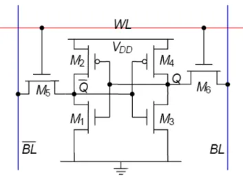
Figure 3. Conventional SRAM Cell.
B. Construction
Conventionally SRAM cells are implemented with 6 transistors known as 6T SRAM (see Fig. 4).
In the traditional 6T-SRAM, the cells must be both stable (during a read event) and writeable (during a write event) ignoring redundancy; such functionality must be preserved for each cell under worst-case variation.
Static RAM is fast as six-transistor configuration of flip-flop circuits keeps current flowing in one direction or the other. The 0 or 1 state can be written and read instantly without any waiting. Each bit in an SRAM is stored on two cross-coupled inverters made from four transistors. This storage cell has two stable states ‘0’ and’1’. Two access transistors serve the purpose of controlling the access to a storage cell during read and write operations. The fewer transistors required per cell, the smaller each cell can be. As the cost of processing a silicon wafer is almost fixed, using smaller cells and packing more bits on one wafer reduces the per bit cost of memory.
Figure 4. Conventional SRAM Cell: 6 Transistor Configuration
SRAM Operation
An SRAM cell has three different states it can be in: standby where the circuit is idle, reading when the data has been requested and writing when updating the contents. The SRAM to operate in read mode and write mode should have "readability" and "write stability" respectively. The three different states work as follows[15]:
• Standby: If the word line is not asserted, the access transistors M5 and M6 disconnect the cell from the bit lines. The two cross coupled inverters formed by M1 – M4 will continue to reinforce each other as long as they are connected to the supply.
• Reading: Assume that the content of the memory is a 1, stored at Q. The read operation is done by using the sense amplifiers that pull the data and produce the output. The row decoders and column decoders are used to select the appropriate cell or cells from which the data is to be read and are given to the sense amplifiers through transmission gate.
International Journal of Electronics Communication and Computer Technology (IJECCT) Volume 3 Issue 5 (September 2013)
ISSN:2249-7838 IJECCT | www.ijecct.org 487
III. SRAM DESIGN AND SIMULATION
Above mentioned configuration of 6T SRAM cell is designed and simulated for 16nm. For CMOS based SRAM cell using Low Power 16nm Metal Gate , High-K , Strained-Si Model, design selection was based on the research [16] by which the M1: M5 strength ratio should be approximately 2.5 (M3&M6) and 0.4 for M2:M5 ratio (M4&M6), for a reliable read and write operation [1].
The Design is then simulated for varying temperature form 5 to 75 degree and 0.5V to 2.0V on hspice. Operating temperature variation could model temperature variation around the year for most part of India and Global operating voltage variation could model a battery discharge in a mobile device.
The corresponding SNM for the designs is calculated and plotted against varying temperature for different operating voltages (see Fig. 5), and against varying operating voltage for different temperatures (see Fig. 6).
Figure 5. SNM of designed cell with varying temperature for different
operating voltages
IV. STABILITY ANALYSIS OF CELL
A.Impact of temperature on cell stability
It has been observed that variations in the operating temperature impact the stability of an SRAM cell. The SNM tends to decrease at the elevated temperatures (see Fig. 5). SNM shows strong virtually linear proportional dependence on the operating temperature variation. Since VTH of 16nm planar CMOS decreases with temperature, the SNM will also decrease with temperature.
B.Impact of supply voltage on cell stability
Stability of the cell is affected by operating voltage. SNM of the cell turned out to be function of supply voltage. SNM tends to increase and then starts to decrease (see Fig. 6). This trend is observed for different temperatures. It is also observed that highest SNM for any temperature is obtained at same operating voltage. Thus there lies an optimized operating voltage for which highest possible SNM can be obtained at any temperature in the range. In our design it turned out to be 1.34 V. Further a method is proposed to calculate this optimized operating point.
V. METHOD FOR CALCULATION
In this paper, we are proposing a method to obtain an optimized operating voltage at which highest possible cell stability is achieved for any temperature in the range.
We are using Static Noise Margin (SNM) as a measure of cell stability. In our observation (see Fig. 5, Fig.6) SNM turned out to be a function of operating voltage and temperature.
In order to obtain optimized operating voltage, we have proposed a method. In this proposed method, SNM at different operating voltage is calculated at room temperature and then optimized operating voltage is calculated for cell design at which the cell will show highest possible cell stability at any temperature in the range.
The methodology is shown below:
1. Initialize cell for hold operation at room temperature. 2. Vary operating voltage from lowest possible value to the highest possible value just before cell hold failure (at room temperature).
3. Plot the result for SNM with operating voltage (see Fig.6) 4. Find the point on graph where |∂ (SNM)/ ∂ (Operating Voltage)| = 0.
5. The point (operating voltage) obtained in step above is the maxima of the curve i.e. point of maximum stability of cell.
6. This operating voltage obtained is the optimized operating voltage at which highest possible cell stability will be obtained at any temperature in the range.
Figure 6. SNM of designed cell with varying voltage for different
temperature
VI. CONCLUSION
International Journal of Electronics Communication and Computer Technology (IJECCT) Volume 3 Issue 5 (September 2013)
ISSN:2249-7838 IJECCT | www.ijecct.org 488 ACKNOWLEDGMENT
The work was performed at Madan Mohan Malviya Engineering college Gorakhpur, U.P. and was partly supported by AICTE research grant F.No. 8023/RIFD/RPS/60/2011-13..
REFERENCES
[1] Pushkarna, A., Sajna Raghavan, and Hamid Mahmoodi. "Comparison of
performance parameters of SRAM designs in 16nm CMOS and
CNTFET technologies." In SOC Conference (SOCC), 2010 IEEE
International, pp. 339-342. IEEE, 2010.
[2] Predictive Technology Models (PTM): http://www.eas.asu.edul-ptml
"16nm PTM LP model: V4.0"
[3] Ebrahimi, Behzad, Saeed Zeinolabedinzadeh, and Ali Afzali-Kusha.
"Low Standby Power and Robust FinFET Based SRAM Design." In
Symposium on VLSI, 2008. ISVLSI'08. IEEE Computer Society Annual, pp. 185-190. IEEE, 2008.
[4] Nii, Koji, Yoshihiro Tenoh, T. O. M. O. A. K. I. Yoshizawa, Susumu Imaoka, Yasumasa Tsukamoto, Y. O. S. H. I. N. O. B. U. Yamagami, T. O. S. H. I. K. A. Z. U. Suzuki, A. K. I. N. O. R. I. Shibayama, H. Makino, and S. Iwade. "A 90 nm low power 32 k-byte embedded SRAM with gate leakage suppression circuit for mobile applications." In VLSI Circuits, 2003. Digest of Technical Papers. 2003 Symposium on, pp. 247-250. IEEE, 2003.
[5] Ishida, M.; Kawakami, T.; Tsuji, A.; Kawamoto, N.; Motoyoshi, M.;
Ouchi, N.; , "A novel 6T-SRAM cell technology designed with rectangular patterns scalable beyond 0.18 μm generation and desirable
for ultra high speed operation," Electron Devices Meeting, 1998. IEDM
'98. Technical Digest., International, vol., no., pp.201-204, 6-9 Dec 1998 doi: 10.1109/IEDM.1998.746322.
[6] Huang, Hong-Yi, and Tzu-Sung Yen. "A low-voltage loadless 4N
SRAM with smart hidden refresh." In SOC Conference, 2003.
Proceedings. IEEE International [Systems-on-Chip], pp. 251-252. IEEE, 2003.
[7] Kulkarni, Jaydeep P., Keejong Kim, Sang Phill Park, and Kaushik Roy.
"Process variation tolerant SRAM array for ultra low voltage applications." In Proceedings of the 45th annual Design Automation Conference, pp. 108-113. ACM, 2008.
[8] Yang, Josh, Baosheng Wang, Yuejian Wu, and André Ivanov. "Fast
detection of data retention faults and other SRAM cell open defects."
Computer-Aided Design of Integrated Circuits and Systems, IEEE Transactions on 25, no. 1 (2006): 167-180.
[9] Yamauchi, Hiroyuki. "A discussion on SRAM circuit design trend in deeper nanometer-scale technologies." Very Large Scale Integration (VLSI) Systems, IEEE Transactions on 18, no. 5 (2010): 763-774. [10] Birla, Shilpi, Neeraj Kr Shukla, Manisha Pattnaik, and R. K. Singh.
"Analysis Of The Data Stability And Leakage Power In The Various Sram Cells Topologies." Analysis 2, No. 7 (2010): 2936-2944.
[11] S. Mukhopadhyay et al., "Device Design and Optimization Methodology
for Leakage and Variability Reduction in Sub-45-nm FD/SOI SRAM," IEEE Trans. Electron Devices, vol. 55, no. 1, pp. 152--162, Jan. 2008.
[12] Singh, Jawar, Jimson Mathew, Saraju P. Mohanty, and Dhiraj K.
Pradhan. "Single ended static random access memory for low-vdd, high-speed embedded systems." In VLSI Design, 2009 22nd International Conference on, pp. 307-312. IEEE, 2009.
[13] A. Bhavnagarwala, X. Tang, and J. Meindl, “The impact of intrinsic
device fluctuations on CMOS SRAM cell stability,” IEEE J. Solid-State
Circuits, vol. 36, no. 4, pp. 658–665, Apr. 2001.
[14] F. L. Yang, J. R. Hwang, and Y. Li, “Electrical characteristic
fluctuations in sub-45 nm CMOS devices,” in Proc. IEEE Custom
Integrated Circuits Conf. (CICC), 2006, pp. 691–694.
[15] Prasad, K. Dhanumjaya Dr MN Giri, and K. Padmaraju Dr M. Raja
Reddy. "Design of Low Power SRAM in 45 nm CMOS Technology." International Journal of Engineering Research and Applications (IJERA) ISSN: 2248-9622 www.ijera.com Vol. 1, Issue 4, pp.2040-2045.
[16] Saibal Mukhopadhyay, Hamid Mahmoodi, and Kaushik Roy “Modeling
of Failure Probability and Statistical Design of SRAM Array for Yield
Enhancement in Nanoscaled CMOS,” IEEE Trans. Computer-Aided
![Figure 1. Comparison of transistor density in logic and SRAM [ITRS 2012], Graph signifies aggressive scaling trends predicted by ITRS in 2012 clearly](https://thumb-eu.123doks.com/thumbv2/123dok_br/16393253.192863/1.893.484.850.719.929/figure-comparison-transistor-density-signifies-aggressive-scaling-predicted.webp)