www.adv-radio-sci.net/11/125/2013/ doi:10.5194/ars-11-125-2013
© Author(s) 2013. CC Attribution 3.0 License.
Radio Science
Best usage of free-space capacitors in ASIC regulators
T. Maier1, D. Droste1, and M. Siegel2
1Robert Bosch GmbH, Reutlingen, Germany
2Karlsruher Institut f¨ur Technologie (KIT), Karlsruhe, Germany
Correspondence to:T. Maier ([email protected])
Abstract.In this work we examine how to improve the per-formance of voltage regulators in application specific inte-grated circuits (ASICs) by placing capacitors into free layout space. The problem arising after layout, when there are ar-eas not covered by functional elements, is where to connect the free-space capacitors (FSCs), as they can be connected to the input or the output net of a voltage regulator. Therefore we designed a testbench for mathematical calculations and one for simulations to identify the influence of a capacitance connected at these certain positions. We mainly focused on PSR analysis while not losing sight of transient effects. The results of calculation and simulation illustrate that the best solution is to split the capacitance half by half to both possi-ble nets if no output capacitance was installed during design. Otherwise a ratio of one to one for input capacitance to out-put capacitance has to be set up for best performance.
1 Introduction
In application specific integrated circuits (ASICs) regulators are used to create an output voltage from a certain input volt-age range. The ideal regulator has a constant output voltvolt-age independent of a load change and without any influence from the input voltage. This influence not only includes DC volt-age levels (line regulation), but also any AC distortion. The independence of the output voltage from the input is called power supply rejection (PSR) (Ong and Chan, 2010). In liter-ature also often the term PSRR (power supply rejection ratio) (Baker, 2010; Holberg, 2010) is found, which is more true for amplifier as there a ratio between the signal amplification and the power distortion damping exists, while in regulators only the power distortion damping is of interest. Nonideal regulators, which are in fact all implemented regulators, suf-fers from both, AC distortions and transient load changes. The PSR is limited in its damping and also frequency de-pendent, i.e. in most cases the PSR gets worse with higher
frequencies due to capacitive coupling. Load changes cre-ate a distortion at the output voltage as the regulation loop needs time to settle to the adoptedIR drop. The investiga-tions of improvement of PSR and load stability are impor-tant, especially if there are sensitive front-ends on the ASIC. They would be disturbed by these effects and then wrong data would be returned by precious analog to digital convert-ers (ADCs) to signal processing devices like on- or off-chip microcontrollers or DSPs. Therefore a better ASIC perfor-mance should be reached by increasing the PSR of the regu-lator.
Many authors have been dealing with topics concerning regulators. New methods to increase PSR or faster load regu-lation loops are e.g. 2-stage reguregu-lation (Yang et al., 2009) or double regulation (Lim et al., 2011). Newest trends also tend to capacitor-less low dropout regulators, where a high PSRR could be reached by an additional fast output buffer, which drives the regulation transistor (Abbasi et al., 2010). Another method to increase PSRR is to add a left-hand zero by nested Miller compensation (Huang and Liu, 2011) or to use a neg-ative feedback loop (Shirahatti et al., 2010). Capacitor-less regulators are voltage regulators, which don’t need an exter-nal bypass or stabilization capacitor as the Texas Instruments TPS78915 (TI, 2000) would need. Nevertheless, capacitor-less does not exclude capacitors at all, as internal capacitors are still used for these regulators. An advantage of on-chip capacitors is that they have very low ESR(QuadTech, 2003) values due to the short metal connections. For on-chip ca-pacitors, often the leakage is stated in the design documents. A typical leakage value is around 1e-8 to 1e-7 A cm−2 (TI, 2009) which would result in a minimum parallel resistance value for 1.8 V and 1 mm2 of around 1.8 G. Smaller ESR value as typical off-chip capacitors and low leakage makes capacitor choice discussion for ESR (Morita, 2011) and leak-age obsolete.
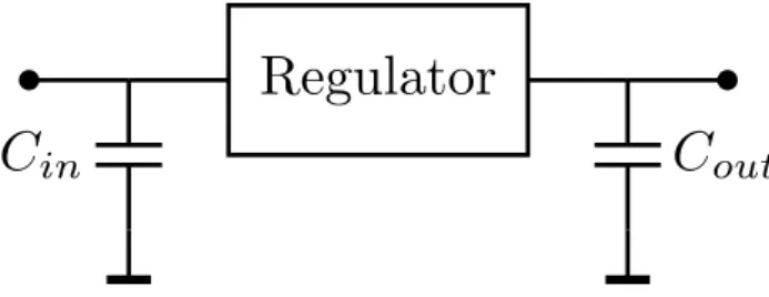
C
in
Regulator
C
out
Fig. 1.Possibel positions for free-space capacitor
voltage with external (TI, 2000) or possible internal capaci-tors are not further investigated.
This work deals with the question, which net is the best to connect free-space capacitors (FSCs). A free-space capac-itor is a capaccapac-itor, created in ASIC areas, which are not cov-ered by functional elements after layout. These areas are of-ten gaps between elements of the regulator. More free space therefore leads to more capacitance. The FSCs are placed into the finished layout and their capacitance values are de-rived from their size, which is then back-annotated from the finalized layout to the corresponding schematic. As a higher capacitance would increase the PSR performance more and the capacitor has no need to have an exact value over pro-cess variations and temperature, the most important parame-ter, when choosing an appropriate capacitor from the design kit, is the capacitance per area. As the functionality of the regulator was already proved through simulations before lay-out, the additional capacitors are used to further improve the regulator and not for stability reasons.
The free-space capacitors are connected to ground with one side in every case, but which is the best net to connect the other side of the capacitors?
Should FSCs be connected to the input or the output net of the regulator (see Fig. 1), or should it be split to both nets? Both nets can be seen as supply nets, which could be stabi-lized by an additional capacitance. There are the same argu-ments for both nets, e.g. the capacitance between a net and ground serves as a low pass, which rejects AC distortions when taking net resistances into account or that FSCs are a charge storage which helps with transient load changes.
It should be mentioned that the reliability of an ASIC should not be decreased by additional free-space capacitors as on-chip capacitors generally have a low leakage. Of course the designer should pay attention that the regulator is still sta-ble with an additional output capacitance, what is normally the case. A capacitor at the input could only have an effect on the time, the regulator needs to start up, if the capacitance is very large. Nevertheless it is worth to re-simulate the reg-ulator after all changes from layout are back annotated.
Regulator Bandgap
Opamp Transistor
Feedback Power Supply
Output
Load
Fig. 2.Regulator under research
2 Regulator under research and testbench
2.1 Regulator under research
For this work, the regulator under research is a low-dropout regulator (LDO), on which the best usage of a free-space capacitor is investigated. The LDO consists of 4 major el-ements, shown in Fig.2. The first one is a bandgap that is used to create a reference voltage to which the output volt-age is compared. Next, there is an operational amplifier (op-amp) which is used to compare the bandgap voltage to the feedback voltage and to set the regulation transistor’s gate voltage corresponding to the result of the comparison. This regulation transistor is the LDO’s third element and is used to regulate the voltage drop between supply net and output net. Generally the transistor can be a n-MOS or p-MOS transistor and here a n-MOS device is used.
The voltage drop thereby is generated through anIRdrop, where the currentI is the current of the load plus the current of the feedback network and the resistanceR is the resis-tance of the transistor,Rdson. This resistance is regulated by
the gate voltage, set by the op-amp. For the regulation tran-sistor it is necessary that its area is big enough so that the maximum current flow density is not exceeded for any load. Large area also helps transporting away the generated heat in the transistor.
The 4th element used in the LDO is the feedback network. In most applications it exists of two resistors forming a volt-age divider, dimensioned in a way that the divided voltvolt-age corresponds to the bandgap voltage, when the output voltage of the LDO has the nominal value (Baker, 2010). The load in this work is a constant resistive load plus a parallel variable current source. An additionally capacitor is also taken into account at the later part of this work.
2.2 Testbench
of the bandgap and the op-amp, connected between the supply wire VDD3V and ground, are included to the test-bench by a impedance Z(s). This impedance is assumed to have one pole, based on simplified simulation results. Including the PSR transfer characteristic of the bandgap ABG(s) and the op-amp Aop(s) is done by the
regula-tion transistor’s gate voltage VG. The Feedback influence
from the resistive voltage divider (VFB) is also included
inVG=Aop(s) (ABG(s) (Vin−Vdrop)−VFB)whereVdrop=
I1(2s Lbond+Rmet)is the voltage drop of the package
cir-cuitry.
3 Calculation and simulation
3.1 Calculations
Based on the testbench, shown in Fig.3 calculations were effected to estimate the results and to verify that the dia-grams gained by simulation show the correct behavior. The testbench has two input variables,VinandIload, but the
cal-culations are done only for Vin as the point of interest is
the PSR analysis. As the results depend on many parameter (e.g.RFB1, RFB2, RL, Rmet, Lbond) only the generalized zero
pole forms are shown in Eqs. (1) and (4). The highest order coefficients of numerator denominator from Eqs. (1) and (4) are shown in Eqs. (2),(3) and (5) respectively, for the param-eters directly affected by the FSCs,CinandCout. All other
parameters are substituted bycniandcdi.
For the frequency behavior ofVDD3V, Eqs. (1),(2) and (3) show that the number of poles and zeros keeps constant if eitherCin orCoutor both are added. This is due toZ(s)
already having a pole, as the additionalCinwould create. But
Eqs. (2) and Eq. (3) show that the poles and zeros are shifted to lower frequencies especially at the change ofCin.
a2,V DD3Vs2+a1,V DD3Vs+a0,V DD3V b4s4+b3s3+b2s2+b1s+b0
(1)
a2,V DD=(cn1Cout+cn2) Cin+cn3Cout+cn4 (2)
b4=(cd1Cout+cd2) Cin2
+(cd3Cout+cd4) Cin+cd5Cout+cd6 (3)
The frequency behavior ofAVDDtoVin(Eq. 4) is similar
to that ofVDD3V (Eq. 1). As both have the same denomina-tor, the poles are shifted the same amount, but Eq. (5) shows that zeros are shifted otherwise.
AV DD Vin
=a2,AV DDs
2+a
1,AV DDs+a0,AV DD b4s4+b3s3+b2s2+b1s+b0
(4)
a2,AV DD=(cn21Cout+cn22+cn23Cin) s2
+(cn24Cin+cn25Cout+cn6) s+cn27 (5)
3.2 Simulation
After the calculations showed the principal behavior, sim-ulations were executed. A simulation testbench was imple-mented, containing the elements added for package and the transistor level circuitry of the bandgap and the operational amplifier. To see the effects of a capacitor added to the in-put or the outin-put clearly, the AC effects of the metal resis-tance and the bond inducresis-tances were simulated separately. AVDD is affected by a metal resistance change only by a pole movement towards lower frequencies. Adding the bond inductances adds a pole at aboutf ∝ 1
Lbond to the transfer
functions, i.e. the higher the bond inductance the lower the frequency of the pole.
The complete regulator is supplied by a voltage of 3.3 V and has an output voltage of 1.8 V. The values for bond in-ductances were zero, 5 nH and 50 nH to see the effect of the inductance. With generally assumed value of≈1 nH mm−1 (Lee, 2003) inductance per bondwire length, a value of 5 nH was used for the later simulations.
The resistance was varied between zero, 5and 50for the simulation of the wire effects. From earlier layout extrac-tions a value of 5 for thick supply wires is assumed for further simulations.
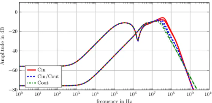
For output transistor a n-MOS transistor is chosen, while the opamp was implemented as folded-cascode. The total ca-pacitance available for connection was extracted from layout with 114 unit capacitors, each with a value of 401 fF. So the total amount of capacitance is around 45.7 pF.
In Fig.4 the AC influence of the free-space capacitor to-wardsVDD3V andAVDD is the point of interest. For the VDD3V net (upper 3 curves) the AC behavior is quite sim-ple. Adding the capacitance to the output net has no effect to the input net in the frequency range of interest. The more capacitance is added to the input net the earlierVDD3V is damped and so has higher damping values at higher frequen-cies. I.e. the more capacitance is added to the netVDD3V, the lower is the frequency of the first pole, what corresponds to the calculation results. Of course the effects onVDD3V directly affectAVDD, asAVDDis derived fromVDD3V.
Vin
Pad
Pad Package
VV DD3V Cin Z(s)
Rds
CGD
CGS gm∗V gs
RF B1
RF B2
VF B
RLIL
RL
CoutVAV DD
VG
Regulator
Load
Fig. 3.Complete testbench for calculation
106
107
108
109
1010
−80 −60
−40 −20 0
frequency in Hz
Amplitude
in
d
B
Cin Cin/Cout Cout
Fig. 4.Effect of FSC to VDD3V and AVDD
is connected to the output net. The additional shift of the in-put net pole towards lower frequencies by the connection of the 2nd half of the capacitance to the input net, helps to im-prove the frequency behavior of the regulator at higher fre-quencies. So splitting could be called the best solution as in mid-frequency range it already damps very well and at high frequencies shows the best damping.
Another point of interest is shown in Fig.5, where again the frequency behavior ofAVDDandVDD3V is shown. The changed parameter now is again the capacity, in this case not only for the additional FSC, but rather for the FSC and a fixed capacitor at the output net. Often a capacitor is installed at the output net for e.g. better transient behavior or stability. There also the question arises where to best connect the additional FSCs.
Again the diagrams were plotted for three cases: All ca-pacitance at the input net (solid curves), all at the output net (dashed-dotted curve) and a half-half split of the capaci-tance(dashed curve).
For the netAVDD(lower 3 curves) the best mid frequency behavior is again reached by connecting all capacitance to the output net. But then the high frequency behavior is very bad because of the missing early pole on the netVDD3V (upper 3 curves), which supplies the regulator. Connecting all the capacitance to the input net leads to very bad mid frequency
106
107
108
109
1010
−80 −60
−40 −20 0
frequency in Hz
Amplitude
in
d
B
Cin Cin/Cout Cout
Fig. 5.Effect of FSC plus add. cap to VDD3V and AVDD
behavior, but a better high frequency behavior as if connect-ing all capacitance to the output. This is due to the earlier pole inVDD3V. With splitting the capacitance, the mid fre-quency behavior is lying between the two other cases but is not much worse as if connecting all FSC to the output. But with split FSCs, AC behavior of netAVDDprofits from the VDD3V pole and therefore shows the same high frequency behavior as if connecting all the FSC to the input. So split-ting is again the best solution.
Simulations show that splitting is best as long as splitting can create an allover ratio of 1 : 1 for all the capacitance at the input net to all the capacitance at the output net. If the output capacitance is greater than the free-space capacitance at all, the best solution is connecting all FSC to the input net. In the diagrams in Figs. 4 and 5 the shape of AC response is only visible in the range between 1 MHz and 10 GHz. In Fig.6 the complete shape is visible for the configuration with a constant capacitance and the free-space capacitance.
100 101
102 103
104 105
106 107
108 109
1010
−80 −60
−40 −20 0
frequency in Hz
Amplitude
in
d
B
Cin Cin/Cout Cout
Fig. 6.Influence of bandgap to AVDD
This simulation is done to prove the necessity to damp the input net, as the bandgap, the operational amplifier and the regulation transistor are connected to that net and so a damp-ing on that net helps improvdamp-ing the output net very much. The diagram also shows that the values of the free-space ca-pacitors are too small to damp the low frequencies where the PSR distortion from bandgap reaches the output net in the range from DC to about 1 MHz.
So far, all the simulations only cover AC behavior and point out how the FSCs influence the frequency behavior. When simulating the transient behavior of load changes, the effects are only very small on the netsAVDD(see Fig.7) and VDD3V. As it can be seen in the diagram, the effect of a load change at the output is almost the same, independent to which net the FSC is connected. The explanation for this ef-fect is that the charge, stored on the capacitor, is very small as the capacitor itself is very small. Therefore the capacitor could only stabilize the voltage for a very short time before the voltage on the capacitor drops together with the output voltage.
4 Conclusions
In this work, we show that it is possible to improve PSR ef-fects of LDOs by the application of FSC during post-layout optimization. We especially point out that FSCs placed half by half to the input and output net of a LDO improve AC performance more than just adding them to one of the two nets. If the LDO already has an output capacitor installed, the best solution is to add capacitance to the input net till the input and output nets have the same amount of capacitance and split the rest of the capacitance.
Splitting the capacitance shifts the main poles of input and output net towards lower frequencies, decreasing PSR effects in mid-frequency range with the output capacitance and in high-frequency range with the input capacitance. It is worth mentioning that due to the small capacitance, placed into the rare free space, the damping AC effects on the output net are also only very small. An additional free-space capacitor also does not have a significant effect on transient load changes.
1 1.2 1.4 1.6 1.8 2 2.2 2.4 2.6 2.8 3 3.2 3.4 3.6 3.8 4
·10−6 1.8
1.85 1.9 1.95 2
time in s
Output
in
V
AVDD Cin AVDD Cin/Cout AVDD Cout
Fig. 7.Transient behavior of AVDD at load change
This work emphasizes, that in contrast to other work, where the focus is on changes in error-amplifier or improve-ment of control loop, a simple, well understood design can still be improved if the cooperation between design and lay-out is excellent and all space on the expensive ASIC is uti-lized.
Therefore the analog designer should already pay atten-tion to post-layout optimizaatten-tion opportunities during design of the circuit to advise layouter where to connect free-space capacitors. An important instrument to fulfill that job is the creation of a proper testbench, containing next to most of the parasitic elements also opportunity devices for post-layout optimization. These could be ideal devices with an estimated value of FSCs which are later replaced by PDK (process de-velopent kit) devices where the real value is back-annotated. This approach is legitimately if the regulator is stable with and without the FSCs and just improved by additional input or output capacitance.
Nevertheless a simulation with extracted parasitics from layout needs to be done in every case.
References
Abbasi, M., Bagnall, D., and Bn, V.: A high PSRR capacitor-less on -Chip low dropout voltage regulator, in: 8th International Sympo-sium on Intelligent Systems and Informatics (SISY), 2010, 361– 364, doi:10.1109/SISY.2010.5647405, 2010.
Baker, R. J.: CMOS Circuit Design, Layout, and Simulation (Third Edition), IEEE Press, doi:10.1002/9780470891179, 2010. Holberg, P. E. A. D. R.: CMOS Analog Circuit Design, Oxfort
Uni-versity Press, 2010.
Huang, W.-J. and Liu, S.-I.: PSRR-enhanced low-dropout regulator, Electron. Lett., 47, 17–18, doi:10.1049/el.2010.2869, 2011. Lee, T.: The Design of CMOS Radio-Frequency Integrated Circuits,
Cambridge University Press, http://books.google.de/books?id= io1hL48OqBsC, 2003.
Ong, G. and Chan, P.: A Low Quiescent Biased Regu-lator With High PSR Dedicated to Micropower Sen-sor Circuits, Sensors Journal, IEEE, 10, 1266–1275, doi:10.1109/JSEN.2009.2038793, 2010.
QuadTech: Equivalent Series Resistance (ESR) of Capacitors, Tech. rep., QuadTech, Incorporated, http://www.low-esr.com/ QT LowESR.pdf, 2003.
Shirahatti, S., Nandi, A., and Priyatamkumar: A Capacitor-less Low Drop out Voltage Regulator, in: IEEE Int. Conference on Com-munication Control and Computing Technologies (ICCCCT), 2010 , 177–182, doi:10.1109/ICCCCT.2010.5670547, 2010.
TI: TPS78915, TPS 78918, TPS78928, TPS78930 Ultralow-Power Low-Noise 100 mA Low-Dropout Linear Regulators Datasheet, Texas Instruments, 2000.
TI: Process Control Document and Design Parametrics for the LBC8 (LinBiCMOS-8) Technology, Texas Instruments, version 2.4, 23 June 2009, 2009.