Effects of the postannealing atmosphere on the dielectric properties of (Ba,Sr)TiO 3
capacitors: Evidence of an interfacial space charge layer
F. M. Pontes, E. R. Leite, E. Longo, J. A. Varela, E. B. Araujo, and J. A. Eiras
Citation: Applied Physics Letters 76, 2433 (2000); doi: 10.1063/1.126367 View online: http://dx.doi.org/10.1063/1.126367
View Table of Contents: http://scitation.aip.org/content/aip/journal/apl/76/17?ver=pdfcov Published by the AIP Publishing
Effects of the postannealing atmosphere on the dielectric properties
of
„
Ba, Sr
…
TiO
3capacitors: Evidence of an interfacial space charge layer
F. M. Pontes, E. R. Leite,a)and E. Longo
Department of Chemistry, UFSCar-Federal University of Sa˜o Carlos, C.Postal 676, 13560-905 Sa˜o Carlos, SP, Brazil
J. A. Varela
Institute of Chemistry, UNESP-Paulista State University, C.Postal 355, 14801-970 Araraquara, SP, Brazil
E. B. Araujo and J. A. Eiras
Department of Physics, UFSCar-Federal University of Sa˜o Carlos, C.Postal 676, 13560-905 Sa˜o Carlos, SP, Brazil
~Received 13 September 1999; accepted for publication 29 February 2000!
The dielectric properties of ~Ba, Sr!TiO3 films were found to be remarkably sensitive to the
postannealing treatment atmosphere. This study demonstrates that postannealing in an oxygen atmosphere increases the dielectric relaxation phenomenon and that postannealing in a nitrogen atmosphere produces a slight dielectric relaxation. Such dependence of the dielectric relaxation was related both to oxygen vacancies and to the presence of negatively charged oxygen, trapped at the grain boundary and/or at the electrode/dielectric film interface. © 2000 American Institute of Physics. @S0003-6951~00!00817-2#
Because of its high dielectric constant, ~Ba, Sr!TiO3 ~BST!1–4
thin film has important potential applications in a variety of technologies that require high charge storage den-sity materials in thin film devices.
The main advantages of~Ba0.6Sr0.4!TiO3are its
paraelec-tric properties in the operating temperature range. It is a gen-erally acknowledged fact that these capacitors, formed by the metal—dielectric—metal configuration, present Schottky barriers at both electrodes~top and bottom!.
Hwang et al.5 reported that different production pro-cesses and processing conditions produce different trap states at the film/electrode interface that are responsible for differ-ent electrical interfacial characteristics. In addition, BST thin films show a remarkable dielectric relaxation phenomenon that strongly affects the dielectric properties of the films.8
Many researches have reported the effect of the postan-nealing treatment under an O2 and/or N2atmosphere in the
behavior of BST film leakage currents. Joo et al.6 have re-ported oxygen vacancies in BST films, obtained by the sput-tering technique, that are usually generated during the pro-duction of Pt/BST/Pt capacitors. These vacancies are responsible for the higher leakage currents of BST films, as well as for the degradation of dielectric properties.7–9 More-over, some recent studies have revealed that electron trap-ping in thin films induces a voltage offset in the polarization-voltage characteristics.10
This letter investigates the influence of postannealing treatments on the dielectric properties of BST thin films, af-ter top electrode deposition, in oxygen and nitrogen atmo-spheres.
~Ba0.6Sr0.4!TiO3 films were prepared by the polymeric
precursor method11–14 and deposited by the spin-coating technique on a Pt/Ti/SiO2/Si substrate. A platinum layer
~140 nm! was used as the bottom electrode. The BST film was then sintered at 700 °C for 2 h in air~film thickness of 480 nm!.
Using the sputtering technique, the 0.3 mm diameter top Au electrode was then deposited through a shadow mask at room temperature. After deposition of the top electrode, the film was subjected to a postannealing treatment in a tube furnace, at 350 °C, in an O2and N2atmosphere for 8 h.
In this work, the first annealing treatment, after BST production, was performed in O2, the second annealing in
N2, and the last in O2. All the postannealing treatments were
carried out on the same sample. Electric measurements were taken after each treatment in different atmospheres. Dielec-tric constant and dissipation factor values, in the 100 Hz–10 MHz frequency range, and capacitance–voltage (C–V) were measured with a HP 4194A impedance analyzer.
ForC–V measurements, a small alternating current sig-nal of 10 mV of amplitude and 100 kHz frequency was ap-plied across the sample, while the direct current~dc!electric field was swept from the positive bias to negative bias and back again. Ferroelectricity was investigated using a modi-fied Sawyer–Tower circuit attached to a Tektronix 2232 digital oscilloscope.
Figure 1 shows the variation of the dielectric constant as a function of frequency for the BST film as-deposited, post-annealed at 350 °C for 8 h in oxygen, second postannealing in nitrogen, and final postannealing in oxygen. It can be ob-served, in Fig. 1, that the sample postannealed in an O2
at-mosphere presents an intense drop in the dielectric constant in the low frequency region~100 Hz–100 kHz!. It is possible that this decrease in the dielectric constant in this frequency range is caused by space charge polarization or Maxwell– Wagner type interfacial polarization. The space charge po-larization is inherently related to the nonuniform charge ac-cumulation. These charges can be originate during the postannealing treatment in an oxygen atmosphere.
a!Electronic mail: [email protected]
APPLIED PHYSICS LETTERS VOLUME 76, NUMBER 17 24 APRIL 2000
2433
0003-6951/2000/76(17)/2433/3/$17.00 © 2000 American Institute of Physics
When the film was postannealed in nitrogen, a reduction of the dispersion of dielectric constant was observed at a low frequency. This result indicates that there was a reduced charge space effect in the dielectric properties. When the film was again postannealed in oxygen, the phenomenon of the space charge polarization appeared and a large dielectric re-laxation was once more observed. This result strongly indi-cates that the dielectric relaxation observed is not a bulk-related phenomenon, but an oxygen-related interface phenomenon.
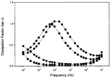
Figure 2 shows the influence of postannealing under dif-ferent atmospheres on the dissipation factor (tand) as a func-tion of frequency for BST films. These curves showed a distinctly visible characteristic peak around the frequency range of 100 Hz–10 kHz when the film was postannealed in oxygen. These curves demonstrate that the oxygen atmo-sphere contributes to the relaxation phenomenon in the di-electric behavior. The curves became flat~Fig. 2!after post-annealing in a nitrogen atmosphere. This result strongly suggests that the relaxation phenomenon arises from the postannealing treatment in an oxygen atmosphere. These re-sults are in agreement with the dielectric constant measure-ment.
Figure 3 shows the relationship between the dc bias and capacitance~C–V curve!applied. Although the curves were measured with both an increasing and a decreasing bias volt-age, only a slight hysteresis was observed in a curve ~ as-deposited!film. This indicates that there is a low concentra-tion of movable ions or charge accumulaconcentra-tion at the interface between the dielectric and the electrode.
TheC–Vcurve showed typical paraelectric behavior for the as-deposited film. On the other hand, when the capacitor was treated in an oxygen atmosphere, the Vm voltage at
which the capacitance is at its maximum Cm value is not
located at the zero bias field, but shifted toward the negative and positive bias region. The higher capacitance, which de-pends on the bias polarity, suggests that the existence of additional capacitance at the interface arises from the space charge, originating from the postannealed film in an oxygen atmosphere.
Two maxima can be observed on the positive side of the C–V curve for the sample postannealed in oxygen, one at 3 V and the other at 1 V. Another maximum can be seen on the negative side of theC–V curve, which may be caused by the presence of some positive charges, such as oxygen vacan-cies. These oxygen vacancies may originate during the pro-cess of heat treatment of the films due to the organometallic decomposition of the polymeric precursor. The negative charges may be associated with the presence of negatively charged oxygen trapped at the grain boundary and/or the film’s electrode/dielectric interface. The negative charge of the oxygen may be caused by charge transference between the metal vacancy and the oxygen, as shown in
VM
9
11/2O2 x⇒VM x
11/2O2
9
, ~1!where Ox,VM
9
,VM x, and O
9
represent, respectively, the neu-tral oxygen ions in their normal position, metal site vacan-cies doubly negatively charged, neutral metal site vacanvacan-cies, and oxygen ions doubly negatively charged.In BST film, theVM must be a barium vacancy (VBa),
since a barium deficiency was identified by an inductively coupled plasma chemical analysis of the precursor solution with an approximate barium deficiency of 3%.
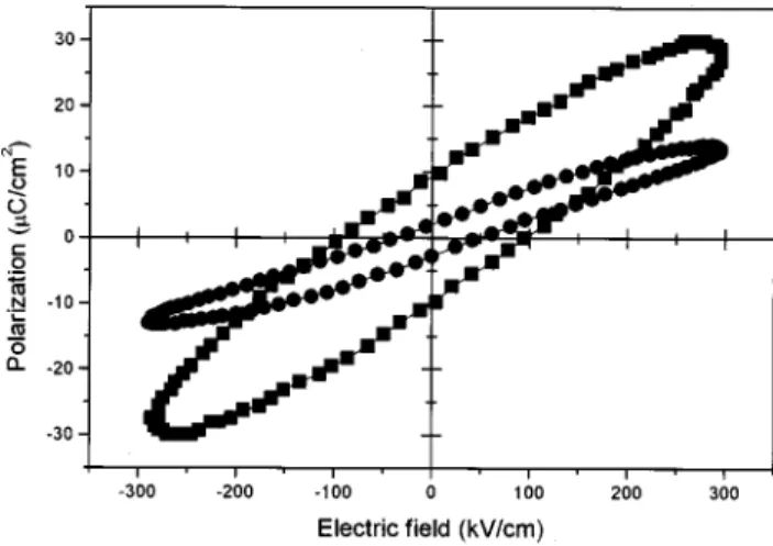
Figure 4 shows the polarization versus electric field (P–E) hysteresis loops of BST films postannealed in differ-ent atmospheres. A typical hysteresis loop, related to
ferro-FIG. 1. Dielectric constant vs frequency characteristics of (.) as-deposited, (l) postannealed in oxygen, (j) postannealed in nitrogen, and (d) post-annealed in oxygen.
FIG. 2. Dissipation factor vs frequency characteristics of (.) as-deposited, (l) postannealed in oxygen, (j) postannealed in nitrogen, and (d) post-annealed in oxygen.
FIG. 3. C–V curve for (j) as-deposited film and (d) postannealed in oxygen.
2434 Appl. Phys. Lett., Vol. 76, No. 17, 24 April 2000 Ponteset al.
electric materials, can be observed. In addition, the crystal-lographic structure of the films was examined using the x-ray diffraction technique ~XRD!, where all the peaks are as-cribed to the cubic perovskite structure. A polycrystalline thin film is observed in the pattern.
A further analysis of the XRD data indicated a lattice parameter~a!ofa50.396 nm. This value is close to the bulk material (a50.3965 nm); thus, the film is by nature paraelectric. This hysteresis is not due to the ferroelectric nature of the film, but rather, to a space charge effect. A slim hysteresis loop is observed after postannealing in nitrogen. This result supports the hypothesis that the hysteresis loop observed stems from the space charge. We believe that the trapped charge (O2
9
) located in the grain boundary or andelectrode/film interface can promove a local stoichiometric deviation. The O2
9
associated with other defects~VO••
or even defect dipole complexes such as oxygen vacancies associeted with barium vacancies VBa
9
–VO••!
located near the grain boundary or and electrode/film interface can promove the hysteresis loops.
In summary, postannealing in oxygen and nitrogen
at-mospheres contributed significantly to the dielectric proper-ties of BST films. Postannealing in an oxygen atmosphere increased the dielectric relaxation phenomenon, while a slighter dielectric relaxation phenomenon was observed when the capacitor was postannealed in a nitrogen atmo-sphere. These results suggest that the postannealing treat-ment in an oxygen atmosphere can increase the trapped charge and the relaxation phenomenon. On the other hand, the results also demonstrate that the best atmosphere for BST films to reach good dielectric properties, free of the relax-ation phenomenon, is postannealing in a nitrogen atmo-sphere.
The authors gratefully acknowledge the financial support of the Brazilian financing agencies FAPESP, CNPq, PRONEX, and CAPES.
1N. Yanase, K. Sano, K. Abe, and T. Kawakubo, Jpn. J. Appl. Phys., Part
237, L151~1998!.
2
S. B. Krupanidhi and C. J. Peng, Thin Solid Films305, 144~1997!.
3
S. Saha and S. B. Krupanidhi, Mater. Sci. Eng., B57, 135~1999!.
4J. C. Shin, J. Park, C. S. Hwang, and H. J. Kim, J. Appl. Phys.86, 506
~1999!.
5C. S. Hwang, B. T. Lee, C. S. Kang, K. H. Lee, H.-J. Cho, H. Hideki, W.
D. Kimm, S. I. Lee, and M. Y. Lee, J. Appl. Phys.85, 287~1997!.
6J. H. Joo, J. M. Seon, Y. C. Jeon, K. Y. Oh, J. S. , and J. J. Kim, Appl.
Phys. Lett.70, 3053~1997!.
7Y. Shimada, A. Inoque, T. Nasu, Y. Nagana, A. Matsuda, K. Arita, Y.
Uemoto, E. Fujii, and T. Otsuki, J. Appl. Phys.35, 4919~1996!.
8
S. Zafar, R. E. Jones, B. Jiang, B. White, P. Chu, D. Taylor, and S. Gillespie, Appl. Phys. Lett.73, 175~1998!.
9Y.-P. Wang, and T.-Y. Tseng, J. Appl. Phys.81, 6762~1997!.
10G. E. Pike, W. L. Warren, D. Dimos, B. A. Tuttle, R. Ramesh, J. Lee, V.
G. Keramidas, and J. T. Evans, Jr., Appl. Phys. Lett.66, 484~1995!.
11M. Liu and D. Wang, J. Mater. Res.10, 3210~1995!. 12V. Agarwal and M. Liu, J. Mater. Sci.32, 619~1997!.
13V. Bouquet, S. M. Zanetti, C. R. Foschini, E. R. Leite, E. Longo, and J. A.
Varela, inInnovative Processing and Synthesis of Ceramic, Glasses, and
Composites, Ceramic Transactions, edited by N. P. Bansal, K. V. Logan,
and J. P. Singh~Am. Ceram. Soc. Inc., Westerville, OH, 1998!, Vol. 85, p. 333.
14S. M. Zanetti, E. R. Leite, E. Longo, and J. A. Varela, J. Mater. Res.13,
2932~1998!.
FIG. 4. P–E hysteresis characteristics of BST film (j) postannealed in oxygen and (d) postannealed in nitrogen.
2435 Appl. Phys. Lett., Vol. 76, No. 17, 24 April 2000 Ponteset al.