JOURNAL OF NANO- AND ELECTRONIC PHYSICS Р А А - А Р
Vol. 8 No 1, 01041(4pp) (2016) Том 8 № 1, 01041(4cc) (2016)
2077-6772/2016/8(1)01041(4) 01041-1 2016 Sumy State University
Comparison of Three Dimensional Partially and Fully Depleted SOI MOSFET Characteristics Using Mathcad
Neha Goel1,*, Manoj Kumar Pandey2,†
1 Research Scholar, SRM University, NCR Campus Ghaziabad, India
2 Department of ECE, SRM University NCR Campus Ghaziabad, India
(Received 23 October 2015; published online 15 March 2016)
In this Paper, comparison of three Dimensional characteristics between partially and fully depleted Silicon-On-Insulator (SOI MOSFET) is presented, this is done through 3D device modeling using mathcad, based on the numerical solution of three dimensional Poisson’s equation. Behavior of Various Parameters like Surface Potential, Threshold Voltage, Electric field and Drain current are presented in this paper.
Keywords: Silicon on insulator (SOI), Poisson’s Equation, Front surface potential, Threshold voltage, Electric field, Drain Current.
DOI: 10.21272/jnep.8(1).01041 PACS numbers: 85.30.tv
*[email protected] †[email protected]
1. INTRODUCTION
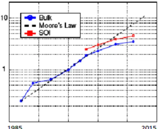
High performance and digital circuits are the cur-rent need of electronics industries, Earlier Bulk MOSFET was considered fit for the electronics industry and to satisfy the Moore’s law [15], which states that performance of transistors in a dense integrated circuit doubles approximately every two years. Primary method to increase productivity and performance is scaling, But due to Short channel effects and junction leakage cur-rent with scaling, it is difficult to follow moore’s law with bulk CMOS. So the need to SOI technology arises [17].
Fig. 1 – Evolution of CMOS Technology with moors Law
2. NEED OF SILICON ON INSULATOR (SOI)
MOSFET
SOI Technology is the solution to the limitation of the CMOS bulk technology against various impacts due to Scale down the device.
There are various characteristics of SOI MOSFET due to which it would be beneficial to switch to SOI MOSFET technology. The main advantages of SOI technology are the following.
Latch can be eliminated as there are no parasitic bipolar devices because of SOI Layer.
Due to the insulation layer above the substrate,
these devices have smaller leakage current. High speed of operation due to the very low
capaci-tance between device and substrate.
Power dissipation of SOI MOSFET is small, because operated at lower voltages and current levels [2].
3. SILICON ON INSULATOR (SOI) MOSFET
Structure of SOI MOSFET is almost similar to that Bulk CMOS, But an insulation layer is inserted under-neath the device on the silicon substrate.
On the Basis of the thickness of the SOI layer, there are Two types of SOI MOSFETS [17]:
1. Partially Depleted SOI MOSFET; 2. Fully Depleted SOI MOSFET.
In Partially Depleted SOI MOSFET, SOI layer Thickness is kept more than the Maximum depletion width of the gate. A technology based on this principle is called a partially depleted SOI Technology. PD SOI Structure is as shown in Fig 2.
Top Silicon Layer is Approximately 50 ~ 200 nm Thick, as per the requirement of the design, Following four parameters Make PDSOI Technology as an essen-tial IC Technology for industry compare to Bulk CMOS. (1) Low Power, Can operate at low power with the same performance. (2) High performance, Provides Perfor-mance gain of 20-40 % [16]. (3) Easy Process (4) Tech-nology mixing. But the major problem with PD SOI is floating body effect.
NEHA GOEL,MANOJ KUMAR PANDEY J.NANO-ELECTRON.PHYS. 8, 01041 (2016)
01041-2
Table 1 – PD and FD SOI Structure at a Glance
Structural
differences Advantages
Partial Depletion
1. Doped Chan-nel
2. Top Silicon 50 ~ 90 nm thick 3. Insulating Box Layer is typically 100 to 200 nm thick
1. Well Under-stood
2. Industrial Proven
3.Easy to Manu-facture.
4. Can leverage floating body for performance gain or memory applications.
Fully Depletion
1. Un doped or lightly doped Channel 2. Top Silicon 5 ~ 20 nm thick 3. Insulating Box Layer may be ultra thin 5 to 50 nm
1. Leakage and power consump-tions are very low
2. for undoped channel, random voltage fluctua-tions can be minimized 3. free from floating body effects
Fig. 3– Fully Depleted SOI MOSFET Structure [14]
In fully depleted SOI MOSFET silicon thickness is very less hence channel is fully depleted from the ma-jority carriers. ie SOI layer is thinner than the deple-tion width of the device [14].
Top silicon layer is approximately 5 ~ 20 nm. Thick, as per the requirement of the design silicon under the gate is very thin so, fully depleted by mobile carriers.
In FD SOI technology, floating point effect can be eliminated as there is no Neutral region of MOSFET for charge [14]. FD SOI Structure is shown in Fig 3 and Comparison points between PD SOI and FD SOI are given in Table 1.
4. DEVICE MODELING
Fig. 4 illustrates a three-dimensional view of a typi-cal MOSFET structure with corresponding device di-mensions. The source-SOI film and drain-SOI film junctions are located at y 0 and y Leff, respectively, where, Leff is the effective channel length. The front and back Si-SiO interfaces are located at x 0 and x ts, where ts is the SOI film thickness. toxf and toxb are
the front and the back gate oxide thicknesses, respec-tively, where the applied potential to the front and back gates are Vgf and Vgb.The vertical and the lateral
direc-tions are defined as x and y, respectively, while the di-rection along the width of the transistor is defined as z. The sidewall Si-SiO interfaces are located at z 0 and z W.
In general, in order to analyze this structure, we have Poisson’s equation, which is as below.
2 2 2
2 , , 2 , , 2 , ,
a
si q N
d d d
x y z x y z x y z
dx dy dz
(1)
In order to solve equation (1), it is separated into 1D Poisson’s equation, 2-&3-D Laplace equation as:
2
2 1
a
si
q N x
d x
dx
(2)
2 2
2 , 2 s , 0
d d
x y x y
dx dy (3)
2 2 2
2 v , , 2 v , , 2 v , , 0
d d d
x y z x y z x y z
dx dy dz (4)
Where, Ψi Ψl(x) + Ψs(x, y) + Ψv(x, y, z) (A)
Main Equation can be obtained by finding separate solutions for Ψl, Ψs and Ψv and finally putting in Equation (A).
Fig. 4– Cross sectional view of double gate SOI MOSFET
along channel length
5. RESULT AND DISCUSSION
Modeling has been done for Both PD and FD SOI MOSFET and comparison between the PD and FD SOI MOSFET’S for Surface Potential, Threshold Voltage, Electric Field with respect to Channel Length is given here, Variation Comparison for Drain current with re-spect to Drain voltage, gate source voltage are also pre-sented as below.
5.1 Surface Potential
com-COMPARISON OF THREE DIMENSIONAL PARTIALLY… J.NANO-ELECTRON.PHYS. 8, 01041 (2016)
01041-3 pare to PD SOI MOSFET.
In the Fig. 5, we determine the variation of front surface potential for n-channel SOI MOSFETs along the different values of channel length at the front Si-SiO2 interface and z w/2. The values we have taken here are: toxf 3 nm, toxb 400 nm, NA 1 1017/cm3 at
Vgf Vgb 0 & Vds 1.5 V.
0.2 0.4 0.6 0.8 1 1.2
0.05 0.1 0.15 0.2 FD PD FD PD
channel length (micrometer)
s ur f a c e po te nt ia l ( V )
i 1 i 2
yi
Fig. 5– Variation of the front Surface Potential along channel
length for PD and FD SOI at the front Si-SiO2 interface
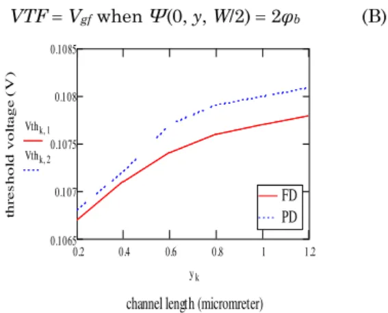
5.2 Threshold Voltage
The Threshold voltage of the short channel MOSFET [5, 11] is defined as the gate voltage at which the minimum surface potential in the channel is the same as the channel potential at threshold for a long channel device, i.e., at threshold.
The variation of threshold voltage with respect to Channel length for PD and FD SOI MOSFET is shown in Fig. 6.
VTF Vgf when Ψ(0, y, W/2) 2φb (B)
0.2 0.4 0.6 0.8 1 1.2
0.1065 0.107 0.1075 0.108 0.1085 FD PD FD PD
channel length (micromreter)
thr e s hol d vol ta ge ( V )
Vthk 1
Vthk 2
yk
Fig. 6– Variation of threshold voltage with respect to channel
length in PD and FD SOI MOSFET
From Fig. 6, It is evident that FD SOI MOSFET is having Lower threshold voltage characteristic as com-pare to PD SOI MOSFET along with the channel length. Hence FD SOI will be less affected by short channel effects.
5.3 Elctric Field
The electric field distribution along the channel length for PD and FD SOI MOSFET is given as below, which shows that FD SOI MOSFET follows higher elec-tric field characteristic as compare to PD SOI MOSFET.
0.2 0.4 0.6 0.8 1 1.2
0 5 10 FD PD FD PD
Channel length (micrometer)
E le c tr ic f ie ld ( V /c m )
Em 1
Em 2
Ym
Fig.7– Variation of electric field along the length of channel for PD and FD SOI MOSFET
5.4 Drain Current
Drain Current is a very important parameter to de-termine the current capacity of any device, this can be considered as a output characteristics of a device. Drain Current Characteristics comparison along with the Drain voltage for PD and FD SOI MOSFET can be shown as below in Fig. 8, This Shows that PD SOI MOSFET is having Kink Effect whereas FDSOI MOSFET is free from any kind of Kinking effect
0 0.5 1 1.5 2
0 5 10 15 PD FD PD FD
Gate to source voltage,Vgs (V)
D ra in C ur r e nt , I d (A )
Idi 1
Idi 2
Vgsi
Fig. 8 – Variation of Dain Current with respect to drain to source voltage in PD and FD SOI MOSFET
Drain Current variation along with gate to source voltage for PD and FD SOI MOSFET, which can also be assumed as input characteristic are shown in Fig. 9. It can be seen here that PD SOI MOSFET shows less Drain Current as compare to FDSOI MOSFET for same value of Vgs.
NEHA GOEL,MANOJ KUMAR PANDEY J.NANO-ELECTRON.PHYS. 8, 01041 (2016)
01041-4
6. CONCLUSION
A 3D modeling and comparison for PD and FD SOI MOSFET has been shown in the paper, this is based on the solution of the Poisson equation. Surface potential, threshold voltage, electric field along with the channel length & Drain Current variations with drain voltage & gate source voltage are given which shows that FD
SOI Performance is giving better Performance results as compare to PD SOI MOSFET.
ACKNOWLEDGMENT
This Research Work is recognized by SRM Universi-ty, Chennai.
REFERENCES
1. C. Fiegna, H. Iwai, T. Wada, T. Saito, E. Sangiorgi, B. Ricco, VLSI Technol. Dig. Tech. Papers33 (1993). 2. Guruprasad Katti, Nandita Das Gupta, Amitava Das
Gup-ta, IEEE T. Electron Dev.51 No 7, 1169 (2004).
3. C. Mallikarjun, K.N. Bhat, IEEE T. Electron Dev.37 No 9, 2039 (1990).
4. Hans van Meer, Kristin De Meyer, IEEE T. Electron Dev.
48 No 10, 2292 (2001).
5. H.K. Lim, J.G. Fossum, IEEE T. Electron Dev. 30 No 6, 713 (1983).
6. Z.H. Liu, C.H. Hu, J.H. Huang, T.Y. Chan, M.C. Jeng, P.K. Ko, Y.C. Cheng, IEEE T. Electron Dev.40 No 1, 86 (1993).
7. Jason C.S. Woo, Kyle W. Terrill, Prahalad K. Vasudev,
IEEE T. Electron Dev.37 No 9, 1999 (1990).
8. Takeshi Shima, Hisashi Yamada, Ryo Luong MoDang, IEEE T. Computer Aided Design of Integrated Circuits
and Systems CAD.2, No 2, (1983).
9. David Esseni, Antonio Abramo, Luca Selmi, Enrico San-giorgi, IEEE T. Electron Dev.50 No 12, 2445 (2003).
10.S. Veeraraghavan, J.G. Fossum, IEEE T. Electron Dev.36 No 3, 522 (1989).
11.Francis Balestra, Mohcine Benachir, Jean Brini, Gerard Ghibaudo, IEEE T. Electron Dev.37 No 11, 2303 (1990). 12.Y.A. El Mansy, A.R. Boothroyd, IEEE T. Electron Dev.24
No 3, 254 (1977).
13.T.Y. Chan, P.K. Ko, C. Hu, IEEE Electron Dev. Lett. 6 No 10, 551 (1985).
14.Neha Goel, Ankit Tripathi, Int. J. Computer Appl. 42 No 21, 975 (2012).
15.https://en.wikipedia.org/wiki/Moore%27s_law. 16.G.G. Shahidi, et al., IEEE Int. Solid- State Circuit
Confe-rence 426 (1999).
17.F.Z. Rahou, A. Guen-Bouazza, M. Rahou, Global J. Res.
Eng. Electrical Electron. Eng. 13 No 1, Version 1.0 (2013).
18.K.W. Temll, C. Hu, P.K. Ko, IEEE Electron Dev. Lett. 5, 440 (1984).
19.Neha Goel, Manoj Pandey, Bhawna Agarwal, Int. J.
![Fig. 3 – Fully Depleted SOI MOSFET Structure [14]](https://thumb-eu.123doks.com/thumbv2/123dok_br/17047223.234012/2.892.85.437.138.748/fig-fully-depleted-soi-mosfet-structure.webp)