J. Nano- Electron. Phys.
3 (2011) No1, P. 474-478 (Sumy State University) 2011 SumDU
474 PACS number: 85.30 De
EFFECT OF GRAIN SIZE ON THE THRESHOLD VOLTAGE FOR DOUBLE-GATE POLYCRYSTALINE SILICON MOSFET
MaheshChandra1, AlkaPanwar2, B.P.Tyag1
1 D B S (Post Graduate) College, Dehradun248001, India
E-mail: [email protected]
2 Chinmhaya College of Sciences, Haridwar, India
The effect of grain size (D) on the threshold voltage (Vth) for double gate polycrystalline silicon MOSFET is investigated theoretically in terms of grain boundary trap states (NT). It is found that the threshold voltage (Vth) increases non-linearly with increasing silicon-oxide thickness (tox) for all values of grain size (D). However the threshold voltage is seen to have smaller values for same tox for the larger grains. This may be attributed to the reduction in the number of trap states in the depletion regions on either side of a grain boundary. Finally the dependence of threshold voltage (Vth) on various parameters such as the doping concentration, interface trap state density and field penetration from drain to source are explored out. The results of these findings are in good agreement with those available in the literature. For large grain poly silicon MOSFET the threshold voltage is seen to approach the single crystal value.
Keywords: DOUBLE GATE POLY SILICON MOSFET, GRAIN SIZE AND THRE-SHOLD VOLTAGE.
(Received 04 February 2011)
1. INTRODUCTION
EFFECT OF GRAIN SIZE ON THE THRESHOLD VOLTAGE… 475
poly Si MOSFET which has shown a well proved performance improvement in terms of the reduced junction capacitance and junction isolation. As a result, the optimization of the channel length is possible which in turn becomes advantageous in carrier transport [7].
The threshold voltage is the most important device parameter for the design, modeling, simulations and utilization of Double Gate Poly Si MOSFET [8]. The threshold voltage in such a device is the minimum gate voltage at which the growth of inversion layer starts. It is common in the literature that the threshold voltage is defined as the gate voltage at which surface potential at the Si SiO2 interface becomes twice the Fermi
potential of Semiconductor body. The threshold voltage for double gate poly silicon MOSFET is the key parameter in the understanding of the device speed and needs to be investigated. In this paper, we present an analytical expression for threshold voltage (Vth) by considering single energy trap level at grain boundary in channel of DG Poly Si MOSFET.
2. THEORY
In order to obtain an explicit expression for threshold voltage (Vth), a single trap energy level is assumed to exist at the grain boundary in Double Gate Poly Si MOSFET [9]. Writing the one dimensional Poisson equation as,
2
2
( )
Si
d x
dx
(1)
Here Si is the permittivity of poly Si. The total charge density (x) is substituted as [10],
( ) 2 sinh T ( , ( )) ( , )
i t f t f
B N q
x q n f E E q f E E
K T D
(2)
Where, Et, Ef and f are the trap state energy level, intrinsic Fermi level and Fermi Dirac distribution factor of electrons for the trap states respectively. D is the average grain size and NT trap states [11]. Thereby,
2
1
2 2 sinh ( , ( ) ( , )
T
i t f t f Si
B N
d q
q n f E E q f E E
dx K T D
(3)
Integrating this equation with boundary condition, that |at interface S one obtains the total charge (QS) per unit area at the interface,
s Si
d QS
dx
(4)
or
1 2
2 ( )
2 4 sinh
2
T T f
s
S B i si
B B i
N E E
q
Q K Tn
K T K Tn D
476 MAHESHCHANDRA, ALKAPANWAR, B.P. TYAG
Now considering the total charge to be the sum of the trap charge (QT) at grain boundary and free charge (Qf) in conduction band.
QS QT + Qf (6)
Since the threshold voltage in DG Poly Si MOSFET is defined as the minimum gate voltage for which induced charge at interface are equal to the trapped charge at the grain boundary, we write,
S T T
Q qN Q (7)
The applied gate voltage VG in DG Poly Si MOSFET is partly dropped across the silicon oxide and partly across the semiconductor bulk material. Thus,
T
G s FB
ox Q
V V
C
(8)
Using equations (7) and (8), one can obtain,
T
G S FB
ox qN
V V
C
(9)
This is the equation for the threshold voltage [10] under the condition when the surface traps have been ignored. However, some traps present at semiconductor silicon oxide interface, causes, a number of fabrication steps in VLSI and hole /electron injection [12, 13]. The distribution, density of surface states can be determined by using methods such as charge pumping and DCIV [14]. The electrons trapped at interface states develop a negative charge at the surface. This negative charge is equivalent to a voltage in opposition to the applied gate voltage, which, can be modeled by a threshold voltage shift toward higher value VGVit. The term Vit is the voltage corresponding to the interface traps [15]. When the value of drain voltage is larger than pinch off voltage, the drain depletion region moves closer to the source depletion region. This result in a significant field penetration from drain to source and the potential at the source is lowered, resulting in an increased injection of electrons over the reduced channel potential barrier. This penetration of the junction electric field into channel region causes barrier lowering which in turn leads to reduction in the threshold voltage [16]. This yield,
0
T ox si
FB it m ds
ox ox
qN
V V V V
C C L
(10)
Where and m are technology dependent fitting parameters, substituting the equation (5) in equation (10), the final expression for threshold voltage Vth is obtained as
1 2
.
( )
2 4 sinh
2
T t f
s i Si
B B i
th
ox
ox Si
s FB it m ds
ox B
N E E
q K Tn
K T K Tn D V
C
V V V
C L
EFFECT OF GRAIN SIZE ON THE THRESHOLD VOLTAGE… 477
3. RESULTS AND DISCUSSIONS
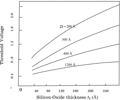
The threshold voltage (Vth) for DG Poly Si MOSFET has been calculated in terms of different parameters and is ploted in figure1 for different value of average grain size (D). The parameters used in these calculation are
0.31, m 2.67, Vit 0.41volts, VFB 1.1 volts, T 300 K, Si 11.9o, ox 3.9o, L 1 µm, Et 0.661 eV and S 2 f, where f is the Fermi potential. For the different values of D the threshold voltage is found to increase non-linearly with increasing silicon-oxide thickness (tox). An increase in threshold voltage is observed with the increasing tox. It may
bedue to reducing gate dielectric field. It is predicted that for large value of D the threshold voltage has smaller value for same tox. This may be attributed to the reduction in the trap states in depletion region on either side of a grain boundary.
Fig. 1 Variation of threshold voltage (Vth) versus Silico – Oxide thickness tox for different grain size D when Vds 0 V
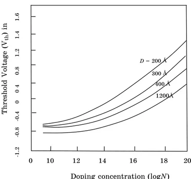
Further investigations, shown in Figure 2, reveal that the threshold voltage increases non-linearly with doping concentration (N) for different values of grain size (D). On the basis of these calculations, the threshold voltage for Double Gate Poly Si MOSFET, with large grain size (D), is found to approach the single crystal value.
4. CONCLUSION
An analytical expression for threshold voltage (Vth) has been forwarded in terms of simple device parameters. The effect of grain size on the threshold voltage for DG Poly Si MOSFET has been explored. The formula is useful in explaining the effects of doping concentration, interface trap state density and field penetration from drain to source on the threshold voltage of the
1200 Å
D 200 Å
300 Å
400 Å
T
h
re
sh
ol
d
V
ol
ta
g
e
(
V
)
in
vo
lt
0
0.
4
0
.8
1.
2
1.
6
2
.0
2
.4
Silicon-Oxide thickness tI(Å)
478 MAHESHCHANDRA, ALKAPANWAR, B.P. TYAG
Fig. 2 Variation of threshold voltage (Vth) versus Doping concentration (N) for different grain size D when Vds 0 V
device. It may finally forwarded that to have DG Poly Si MOSFET with larger values of threshold voltage, one must either increase the interface trap state density or apply a negative bias on back gate.
REFERENCES
1. C.H. Shih, J.S. Wang, IEEE Electr. Device L. 30, 278 (2009).
2. J.W. Han, C. Kim, Y.K. Choi, IEEE T. Electron. Dev.55, 1472 (2008).
3. A. Sehgal, T. Mangla, M. Gupta, R.S. Gupta, proc. of ASID`06, 2006, New Delhi, India. 4. F.T. Chien, C.N. Liao, C.M. Fang, Y.T. Tsai, IEEE T. Electron. Dev.56, 441 (2009). 5. F. Lime, B. Iniguez, O. Moldovan, IEEE T. Electron. Dev.55, 1441 (2008).
6. J.B. Roldan, A. Godoy, F. Gamiz, M. Balaguer, IEEE T. Electron. Dev.55, 411 (2008). 7. J.A. Lopez-Villanueva, F. Gamiz, J. Banquri, A.J. Palma, IEEE T. Electron. Dev.
47, 141 (2000).
8. A.O. Conde, F.J.G. Sanchez, M. Guzman, Solid State Electron.47,2067 (2003). 9. M. Chandra, R. Kumar, B.P. Tyagi, National Seminar on Nano- Sized Semiconductor
Materials, 2009, Pune, India.
10.C.H. Kim, K.S. Sohn, J. Korean Phys. Soc.28, 620 (1995). 11.B.P. Tyagi, K. Sen, phys. stat. sol. A85,603 (1984).
12.A.E. Parker, Ph.D. Dissertation, University of Sydney (1990).
13.C.J. Zhao, J.F. Jhang, J.N. Ellis, C.D. Beech, J Appl. Phys.90,328 (2001). 14.V. Tilak, K. Matocha, G. Dume, E.O. Sveingbjornsson, IEEE T. Electron. Dev. 56,
162 (2009).
15.S. Zaman, E.E. Parker, 3rd International conference on electrical and Computer engineering IGECE 2004, 2004, Dhaka, Bangladesh.
16.S. Chopra, R.S. Gupta, Microelectron. Eng.54,263 (2000). D = 200 Å
400 Å 300 Å
1200Å
-1.
2
-0.
8
-0.
4
0
0
4
0.
8
1.
2
1.
4
1.
6
T
h
re
sh
ol
d
V
ol
ta
g
e
(Vth
)
in
Doping concentration (logN)