www.adv-radio-sci.net/4/281/2006/ © Author(s) 2006. This work is licensed under a Creative Commons License.
Radio Science
Modelling of the parametric yield in decananometer SRAM-Arrays
Th. Fischer1, T. Nirschl2, B. Lemaitre2, and D. Schmitt-Landsiedel1
1Lehrstuhl f¨ur Technische Elektronik, Technische Universit¨at M¨unchen, M¨unchen, Germany 2Infineon Technologies AG, M¨unchen, Germany
Abstract. In today’s decananometer (90 nm, 65 nm, . . .), CMOS technologies variations of device parameters play an ever more important role. Due to the demand for low leak-age systems, supply voltleak-age is decreased on one hand and the transistor threshold voltage is increased on the other hand. This reduces the overdrive voltage of the transistors and leads to decreasing read and write security margins in static mem-ories (SRAM). In addition, smaller dimensions of the de-vices lead to increasing variations of the device parameters, thus mismatch effects increase. It can be shown that local variations of the transistor parameters limit the functional-ity of circuits stronger than variations on a global scale or hard defects.
We show a method to predict the yield for a large number of SRAM devices without time consuming Monte Carlo sim-ulations in dependence of various parameters (Vdd, temper-ature, technology options, transistor dimensions,. . .). This helps the designer to predict the yield for various system op-tions and transistor dimensions, to choose the optimal solu-tion for a specific product.
1 Introduction
With the scaling of modern VLSI circuits according to Moore’s law and the ITRS (ITRS , 2005) new problems arise. The smaller dimensions of transistors in advanced CMOS technologies allow the circuits to consume smaller chip area and to operate at higher clock rates. But on the other hand the standby power consumption is rising due to higher leak-age currents. Short channel effects increase the sub-threshold leakage and with the thinner gate oxides of scaled-down tran-sistors the gate leakage is also increasing.
Therefore, today many systems operate at lower supply voltages and the threshold voltages of the transistors
in-Correspondence to: Th. Fischer ([email protected])
crease, resulting in a lower power dissipation. However, the functionality of many circuits depends on this decreas-ing overdrive voltage, i.e. VDD−Vt h. Hence the read and the write security margins of static memory devices (SRAM) are decreasing.
On the other side the variations of the device characteris-tics (e.g. transistor length and width, threshold voltage) are ever more increasing with proceeding technologies. Print-ing these small devices gets harder due to the subwave-length lithography used in todays semiconductor industry. Also the statistical variation of the dopant concentration un-der the gate of a MOSFET transistor increases with smaller dimensions.
With emerging technologies the share of static random ac-cess memory (SRAM) gets larger with every generation. Due to the large demand of memory, SRAM cells must be de-signed as small as possible, and the cell area is an important benchmark for the quality of a design shrink. The large num-ber of SRAM cells on a System on a Chip (SOC) and the usage of minimum feature size transistors makes the SRAM cell an ideal device for the characterization of variation ef-fects and a good vehicle for yield testing.
In the following section, local and global variations are de-scribed. In Sect. 3 the read and write margins of SRAMs are introduced. Sections 4 and 5 present a method to model the parametric yield using a worst case distance analysis. Sec-tion 6 shows some results of the yield analysis and is fol-lowed by a summary.
2 Local and global variations
BL BLB
WL
Vss Vdd
WL
PD1
PL2
PD2 PL1
’1’ ’0’
S
SB PG1
PG2
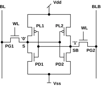
Fig. 1. A 6T SRAM core cell with the two pass gate n-FET
transis-tors (PG1,2), the two pull down n-FET transistransis-tors (PD1,2) and the two p-FET pull up transistors (PL1,2).
to all devices of a die. An example for this type of variations is the oxide thicknesstox or a variation of the widthW and lengthLof the devices due to a global misalignment of the masks. Also the threshold voltageVt hof all the transistors on a die can be shifted by a constant value. These variations are of systematic nature. They can be improved during pro-duction with a tighter process control, and the impact of the global variations can be attenuated during design with layout techniques such as symmetry of important devices.
Local variations rom device to device are known as device mismatch. This are stochastic variations, such as the number of dopants under the gate area of a MOSFET device. These variations increase with smaller area of a device. Pelgrom et al. (1989) shows that the variation of the threshold voltage
Vthobeys the following equation:
σVt h =
AVt h
√
W L (1)
where W is the width and L is the length of the transis-tor. AVt h is the matching constant for the threshold voltage. The variaton of the transconductance factorβ=µCoxW/L is modeled in a similar way:
σβ
β =
Aβ
√
W L (2)
In this caseAβ, is the process related matching constant for the transconductance factor.
The only way a designer can improve the matching of the devices is to improve the area.
0 0.2 0.4 0.6 0.8 1 1.2
0 0.2 0.4 0.6 0.8 1 1.2
VSB
VBLB
Writelevel = 0.33V
⑥
❜ ❜ ❜ ❜ ❜ ❜ ❜ ❜ ❜ ❜ ❜ ❜ ❜ ❜ ❜ ❜ ❜
❜ ❜ ❜ ❜ ❜ ❜ ❜
Fig. 2. Voltage at the storage nodeVSBwhile loweringVBLB. The
core cell has a Write Level of 0.33 V.
3 Read and write margin of SRAM cells
Figure 1 shows a 6-transistor SRAM core cell. During read access the bitlines BL and BLB are charged to a pre-charge level – usuallyVDD. For further discussions we as-sume a ’0’ stored in the storage node S at the BL side. When opening the access devices PG1 and PG2, the voltage level on the storage node S at the bitline side rises due to the voltage-divider formed by the transistors PG1 and PD1. The cell ratio CR is defined as
CR= WP D/LP D WP G/LP G
(3) and sets the voltageVSon the storage node. When this volt-ageVS rises above the switching level (SWL) of the cross coupled inverters of the SRAM core cell, the cell looses its data while reading the cell. This is called destructive read. In this work, the static noise margin (Seevinck et al., 1987) is used to measure the stability of the SRAM core cell dur-ing read access. A destructive read occurs when the SNM drops to zero or below. Another performance measure of the SRAM core cell is the read currentIreadthrough the
transis-tors PG and PD.
When writing a ’0’ to the storage node SB on the BLB side of the core cell, the voltage on BLB is lowered to 0. Here the voltageVSB on the storage node SB is defined by the voltage-divider formed by the transistors PL2 and PG2. Analog to the read case a pull-up ratio PR can be defined as
P R=WP U/LP U WP G/LP G
. (4)
While lowering the voltage on BLB, the write level is defined as the value of the BLB when the cell flips (see Fig. 2). If the write level is larger than 0 the cell can be written.
-3 -2 -1Parameter 1 0 1 2 3-3
-2-1
0
1 2
3
Parameter 2 0
0.2 0.4 0.6 0.8 1 pdf(Parameters)
−3 −2 −1 0 1 2 3
Parameter 1
−3 −2 −1 0 1 2 3
Parameter 2
Specification boundary
Worst Case Point Worst Case
Distance Nominal Point
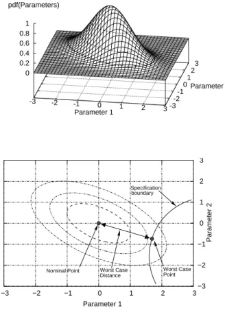
Fig. 3. Schematic probability density of two transistor parameters
(top) and worst case distance and worst case point with specification boundary (bottom).
4 The worst case analysis
In order to define the yield of an SRAM core cell array the Worst Case Distance Analysis is used (Antreich et al., 1994). Simply spoken, the Worst Case Distance is a proba-bility measure for the most likely violation of a performance specification. In Fig. 3 the parameter space of a circuit is symbolized. For example, the parameter space can be the lo-cal threshold voltage and mobility variations of all six tran-sistors of an SRAM core cell. Here only two parameters are shown in thex−y-plane. Thez-axes shows the probability density of the parameter space.
For every parameter-set a performance can be simulated with the according parameters as input for the circuit simu-lator. Now a specification for a circuit performance can be defined. On the top of Fig. 3 we see the top view of the prob-ability density function. The solid line represents a specifica-tion boundary. This is given by all parameters sets that result in the same specified performance value. Everything right of the specification boundary violates the specification and results in an non-functional SRAM core cell.
The smallest distance between the nominal point, i.e. the parameter set with the highest probability, and the
0 0.1 0.2 0.3 0.4 0.5 0.6 0.7 0.8 0.9 1
3 3.5 4 4.5 5 5.5 6
Yield
Worst Case Distance 32 kBit
256 kBit 1 MBit
Fig. 4. Yield vs. Worst Case Distance of local variations for
differ-ent SRAM core cell array sizes.
tion border is the worst case distance WCD. The point on the specification border that is closest to the nominal point has the highest probability that a parametric fault occurs.
The WCD can be translated into a probability of a func-tional core cell array:
Yield= 1
2 1+erf WCD
√
2 !!!N
(5)
where N is the number of core cells in an array. In or-der to achieve a yield of 90% for a 1MBit SRAM array a WCD of 5.2 (see Fig. 4) must be reached or redundancy must be used.
5 First global than local
In order to find the yield of an SRAM array, global and lo-cal variations must be simulated independently. First a set of global parameters must be found that represent the worst die in the production process — not including mismatch. There-fore only parameters that define global variations are con-sidered for analysis, e.g. the oxide thicknesstox, the global fluctuations of the n-FET and p-FET threshold voltageVthn
andVthpand the length and width variations of the devicexL andxW. For a given statistical variation of a process, the al-gorithm looks for the set of the global parameters that results in the worst performance of the core cell.
Once the parameter set for the worst die is found, an anal-ysis of the local variations in an SRAM cell can be made. The local parameters considered in this work were theVt h variations and the mobility variations of the six transistors in the core cell. Hence 12 local parameters were taken into account.
!0.4
!0.2 0 0.2 0.4 0.6 0.8 1
0.8 0.85 0.9 0.95 1 1.05 1.1 1.15 1.2
Worst case write level (a.u.)
Vdd
Worst Case Write Level 25C
0 sg. 1 sg. 2 sg. 3 sg. 0 sg. 5.s sl. 1 sg. 5.s sl. 2 sg. 5.s sl. 3 sg. 5.s sl. global variation
local variation
Fig. 5. Worst Case Write Level for global and local variations.
Vari-ations in sigma global (sg.) and sigma local (sl.).
For this task we used a tool called WiCkeD from Muneda (http://www.muneda.com). This tool uses an sequential quadratic programming (SQP) algorithm to find the Worst Case Distance (Antreich et al., 2000). An external TCL script was used to control the WicKeD program to run the worst case distance analysis first with just global variation, and then with local variations using the worst case parameters obtained by the global WCD analysis. A SPICE simulator simulated the performances of the SRAM core cell for a set of parameter values, and a Perl script wrote the simulation results back to WiCkeD for further evaluation.
Two modes of an analysis of the parametric yield are real-ized. First of all, a WCD can be found by defining specifica-tions for each performance, like Write Level or Static Noise Margin. On the other hand it is possible to look for the worst performance in an array of a given size. For that purpose a WCD is chosen according to the SRAM array size. Then the parameter set for the worst performance with the given WCD is searched for.
6 Results and performance
For the simulation of the SRAM performances, the BSIM4 parameters of an 65 nm technology (Luo et al., 2002) were used. First of all, the influence of global and local varia-tions on SRAM core cell performances were simulated. In Fig. 5 we see a normalized plot of the Write Level of an SRAM core cell for different supply voltages. The upper set of lines shows the relative worst case Write Level depend-ing on global variations rangdepend-ing from 0 to 3 sigma. With the worst case parameter-set found by the global simulation, a simulation for the worst case performance using just lo-cal variations such as theVt hand the mobilityµfor the six core cell transistors was made. The local worst case distance
0.1 0.2 0.3 0.4 0.5 0.6 0.7 0.8 0.9 1
0.8 0.85 0.9 0.95 1 1.05 1.1 1.15 1.2
Worst case distance (a.u.)
Vdd Worst Case Distances
Write level -40C Static noise margin 120C Iread -40C
Fig. 6. Worst Case Distances for the write level, the static noise
margin and the iread of a SRAM cell. All temperatures are the worst case temperatures.
WCD of 5.2 sigma was chosen to represent a SRAM core cell array with 1 MBit (see Fig. 4).
The local variation has a large influence on the function-ality of the SRAM array due to two effects. First the large number of core cells that must be fulfill the specifications in order to get a SRAM array with 100% working cells. Second the smaller size of the transistors increase the local varia-tions and with lower overdrive voltage result in more core cells failing the specification.
Although the local variations are more dominant, one can see form Fig. 5 that a tighter process control can result in circuits operating at a lower supply voltage.
To identify the performance that is the main yield detrac-tor, the worst case distances of the write level, the static noise margin and the read current were simulated. The circuit is simulated with the temperature corners of the specifica-tion that results in the respective worst performance. This is -40◦C for the write level and the read current and 120◦C for the SNM. So the worst cases of the performances are compa-rable. It is shown in Fig. 6 that different performances limit the yield of the core cell. For high supply voltages the read stability (SNM) is the main yield detractor, whereas the write level limits the yield for supply voltages lower than 1.1V, and the read current is the yield detractor for the low voltage operation.
figures show clearly that simulations of parametric yield can be simulated much faster with the Worst Case Distance anal-ysis. Therefore multiple yield simulations with multiple parametric variations, such as temperatures, supply voltages and even different transistor sizes, can be done and used for design centering and verification considering global and lo-cal variations.
7 Conclusions
We presented a method to effectively simulate the yield and the worst case corners of several SRAM performances. This Worst Case Distance Analysis is by 6 orders of magnitudes faster than a Monte Carlo Analysis. So a six-sigma simula-tion can be done for several parameter alterasimula-tions of a circuit. It is possible to find the main yield limiting performances for the worst case operating conditions. This gives the circuit designer a tool to simulate different transistor sizing options under the influence of global and local parameter variations.
References
ITRS, International Technology Roadmap for Semiconductors 2005 Edition,http://public.itrs.net/
Pelgrom, M., Duinmaije, A., and Welbers, A.: Matching Properties of MOS Transistors, IEEE J. Solid State Circuits, 24, 1433–1440, 1989.
Seevinck, E., List, F., and Lohstroh, J.: Static Noise Margin Analy-sis of MOS SRAM Cells, IEEE J. Solid State Circuits, 22, 525– 536, 1987.
Antreich, K., Graeb, H., and Wieser, C.: Circuit Analysis and Opti-mization Driven by Worst Case Distances, IEEE Transactions on Computer-Aided Design of Integrated Circuits and Systems, 13, 57–71, 1994.
Antreich, K., Eckmueller, J., Graeb, H., Pronath, M., Schenkel, F., Schwencker, R., and Zizala, S.: WiCkeD: Analog Circuit Syn-thesis Incorporating Mismatch, IEEE Conf. on Custom Inte-grated Circuits, 511–514, 2000.