Vol. 6, No. 1, May 2009, 33-42
High Speed Multiplier Design
Using Decomposition Logic
Palaniappan Ramanathan, Ponnisamy Thangapandian Vanathi,
Sundeepkumar Agarwal
1Abstract: The multiplier forms the core of a Digital Signal Processor and is a major source of power dissipation. Often, the multiplier forms the limiting factor for the maximum speed of operation of a Digital Signal Processor. Due to continuing integrating intensity and the growing needs of portable devices, low-power, high-performance design is of prime importance. A new technique of implementing a multiplier circuit using Decomposition Logic is proposed here which improves speed with very little increase in power dissipation when compared to tree structured Dadda multipliers. Tanner EDA was used for simulation in the TSMC 180nm technology.
Keywords:Digital Signal Processor, Dadda multiplier, Decomposition Logic.
1 Introduction
With ever increasing applications in mobile communications and portable equipment, the demand for low-power, high-performance VLSI systems is steadily increasing. Digital signal processors and application specific integrated circuits rely on the efficient implementation of arithmetic circuits (adder and multiplier) to execute dedicated algorithms such as convolution, correlation and filtering [1]. A multiplier design using decomposition logic is presented here which improves speed when compared to the tree structured Dadda multiplier with very little power penalty. Pipelining is often used to improve the throughput of a design. A novel concept of modifying an adder to have latched outputs is presented to reduce the overheads of implementing pipelined structures.
2
Tree Structured Multiplier Design
The two well-known tree multipliers are those presented by Wallace [8] and Dadda [2]. Wallace showed that the delay for an N×N multiplier can be reduced to logN, making it faster than the array multiplier. In Wallace’s
1
Department of Electrical and Engineering, University of Bechar, Algeria E-mail: othmane08000@yahoo.fr
method, a pseudo-adder (a row of N full adders with no carry chain) is used to sum three operands into a two operand result with only one single full adder delay [4]. The procedure is repeated continuously to generate two rows of partial products from N row partial products for an N×N multiplier. These two rows are then combined using a fast carry propagating adder (CPA).
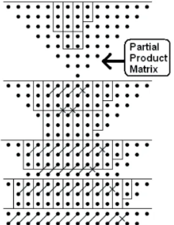
Dadda generalized and extended Wallace’s results by noting that a full adder can be thought of as a circuit which counts the number of ones in the input, and then outputs that number in 2-bit binary form [4]. Using such a counter, Dadda postulated that, at each stage, only minimum amount of reduction should be done in order to reduce the partial product matrix by a factor of 1.5. In the Wallace method, the partial products are reduced as soon as possible. In contrast, Dadda’s method does the minimum reduction necessary at each level to perform the reduction in the same number of levels as required by the Wallace method resulting in a design with fewer full adders and half adders. The disadvantage of Dadda’s method is that it requires a slightly wider, fast CPA and has a less regular structure than Wallace’s. Fig. 1 shows an 8×8 multiplier designed using Dadda’s method.
Fig. 1 – Dadda multiplier for 8×8 multiplication.
3 Decomposition
Logic
4
Design of Multiplier using Decomposition Logic
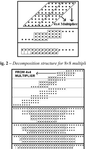
To evaluate the performance of the new multiplier structure, 8×8 and 16×16 multiplier structures were designed using Dadda’s method and the decomposition logic. A CPL adder [6] was used in all the designs due to its better performance than other adders in tree structured designs.Fig. 2 shows an 8×8 multiplier implemented using the decomposition logic. In the first stage, four 4×4 multipliers are used to combine all the partial products. The outputs from these 4×4 multipliers are then combined in a treelike fashion to get the final results. The 4×4 multiplier was implemented using Dadda’s method [3]. For 16×16 multiplication, three decomposition structures are possible. The first using 4×4 Dadda multipliers, the second using 8×8 Dadda multipliers and the third using 8×8 decomposition structure as shown in Figs. 3 and 4.
Fig. 2 –Decomposition structure for 8×8 multiplication.
Fig. 4 – Decomposition structure for 16×16 multiplication using 8×8 multipliers.
5
Design of 8
×
8 Pipelined Multiplier
Pipelining is a popular design technique often used to accelerate the operation of datapaths in digital signal processors. Two pipelined multiplier structures are presented here; one using separate latches and the other using a novel concept of designing a full adder with latched outputs. Pipelined circuits can be constructed by using level sensitive latches at the output of intermediate stages. A static latch derived from PowerPC flip-flop [7] is shown in Fig. 5 and named ‘PowerPC latch’ for reference. It uses a transmission gate controlled by a clock signal at the input. The feedback path consists of an inverter and a transmission gate combined together to reduce power dissipation.
To reduce the overheads (transistor count and power dissipation) of implementing pipelined multiplier design, a latched adder is proposed by modifying the CPL adder. The latched CPL adder is shown in Fig. 6. The latch portion of the adder is derived from a two phase CPL flip-flop structure [5]. The structure is pseudo-static and requires only single phase clocking as opposed to the two phase clocking required for the PowerPC latch. The latched version requires only two extra transistors when compared to the CPL adder. When the PowerPC latch is used at the output of the adder, 10 transistors are needed. Hence, 8 transistors are saved by using the Latched CPL adder as compared to PowerPC latch.
CLK
CLKB
CLK CLKB
D Q
Qb
Fig. 5 – PowerPC Latch.
A
B
B Ab
Bb
A
Ab
Bb
F
Fb C
Cb
Cb
C F
F
CLK
CLK
S
Sb
Fig. 6 – Latched CPL adder.
6
Simulation Environment
comparison are power consumption, worst case delay and energy-delay product. Delay was calculated from 50% of input voltage level to 50% of output voltage level. Energy-delay product was chosen to put more emphasis on the speed performance of the circuit.
The two pipelined 8×8 Decomposition multipliers were simulated at different voltages ranging from 1.0V to 1.8V. The worst case delays of the two structures differed by a negligible value. So the two structures were then compared for their power dissipation values and number of transistors needed.
7 Results
The simulation results for 8×8 multipliers are summarized in Table 1. For the 8×8 multiplier structure, the decomposition logic shows an improvement of 22% to 25% in delay compared to Dadda’s method due to parallel processing of data. The power dissipation is slightly less than that of the Dadda structure due to reduction in glitches in spite of the extra logic circuitry. The energy-delay product is reduced by more than 41%. The energy-delay product for 8×8 multiplier structures is shown in Fig. 7.
Table 2 shows the results for the 16×16 Dadda multiplier and the 16×16 Decomposition multiplier designed using 8×8 Dadda multiplier. The decomposition logic shows a delay reduction of about 17% to more than 40% depending upon the supply voltage. Despite the power dissipation being slightly more than the Dadda structure, the energy-delay product is 30% to 64% lesser than that of the Dadda structure. The energy-delay product for the 16×16 multiplier structures is shown in Fig. 8.
As mentioned earlier, three decomposition structures are possible for 16×16 multiplication. An analysis was done to choose the best decomposition structure. Table 3 shows the results for the three decomposition structures. The values are normalized for better understanding. It is seen that power dissipation decreases with an increasing level of decomposition while the delay increases. The reduction in power consumption is due to a lesser number of glitches when there is more parallel processing. But the delay increases due to extra logic circuitry which outweighs the benefits derived from parallel processing. So, for high performance, the 16×16 decomposition structure designed using four 8×8 Dadda multipliers (having one decomposition level) has to be chosen. Table 4
Table 1
Simulation results for 8×8 multiplier.
Power (µW) Delay (ns) Energy-delay
product (10-21 Js) Supply
voltage
(V) Decom-
position Dadda
Decom-
position Dadda
Savings %
Decom-
position Dadda
Savings %
1.8 567 569 1.12 1.51 25.83 0.71 1.29 44.96
1.5 184 189 1.45 1.92 24.48 0.38 0.69 44.93
1.2 112 117 2.51 3.23 22.29 0.71 1.22 41.80
1.0 76.7 80.8 4.00 5.19 22.93 1.23 2.18 43.58
Table 2
Simulation results for 16×16 multiplier.
Power (mW) Delay (ns) Energy-delay product (10-21 Js) Supply
voltage
(V) Decom-
position Dadda
Decom-
position Dadda
Savings %
Decom-
position Dadda
Savings % 1.8 2.774 2.696 1.41 1.71 17.54 5.51 7.88 30.04 1.5 0.933 0.890 2.00 2.85 29.82 3.73 7.23 48.37 1.2 0.569 0.533 3.18 5.46 41.76 5.75 15.9 63.79 1.0 0.196 0.183 5.05 8.71 42.02 4.99 13.9 64.00
Table 3
16×16 Multiplier Using Decomposition Logic.
Normalized Power Normalized Delay Supply
voltage (V)
Using 8×8 Dadda
Using 8× 8 Decomposition
Using 4× 4 Dadda
Using 8× 8 Dadda
Using 8× 8 Decomposition
Using 4× 4 Dadda
1.8 1.00 0.92 0.90 0.90 0.98 1.00
1.5 1.00 0.92 0.91 0.63 0.79 1.00
1.2 1.00 0.91 0.90 0.55 0.72 1.00
1.0 1.00 0.91 0.89 0.56 0.73 1.00
Table 4
Transistor count for multiplier structures.
Decomposition Dadda 8× 8 multiplier
1648 1476 Decomposition
Using 8× 8 Dadda
Using 8× 8 Decomposition
Using 4× 4 Dadda
Dadda 16× 16 multiplier
0 5E-22 1E-21 1.5E-21 2E-21 2.5E-21 E n er g y-d el ay P ro d u ct ( J s)
1.8 1.5 1.2 1
Supply Voltage (V)
8x8 MULTIPLIER
Decom-position
Dadda
Fig. 7 – Latched CPL adder.
0.00E+00 2.00E-21 4.00E-21 6.00E-21 8.00E-21 1.00E-20 1.20E-20 1.40E-20 1.60E-20 E n er g y-D el ay P ro d u ct ( Js)
1.8 1.5 1.2 1
Supply Voltage (V)
16x16 MULTIPLIER
Decom-position
Dadda
The simulation results for the two pipelined multiplier structures are shown in Table 5. It can be observed that the latched CPL adder reduces the overhead for pipelined structures when compared to the use of separate latches for pipelined multiplier design.
Table 5
Simulation results for 8×8 pipelined multiplier structures.
Power Results
Supply Voltage (V) Latched CPL Adder
(µW) PowerPC Latch (µW) Savings %
1.8 652 720 9.444
1.5 422 470 10.21
1.2 125 142 11.97
1.0 85.6 98.5 13.09
Transistor Count
Latched CPL Adder PowerPC Latch Savings % No. of Transistors
1840 1976 6.882
8 Conclusion
A new technique of implementing digital multipliers using decomposition logic is presented here. When compared to the Dadda multiplier, the proposed multiplier was faster and energy efficient with a negligible power penalty in spite of extra logic circuitry. A guideline to choose the appropriate decompo-sition structure for larger multipliers has also been provided. A pipelined implementation of the decomposition multiplier structure has been presented, using a new concept of adders having latched outputs which reduces the overhead costs in pipelined implementations. The decomposition logic presen-ted here can be extended to other multiplier designs such as the Booth multiplier.
9 References
[1] C.H. Chang, J. Gu, M. Zhang: A Review of 0.18µm Full Adder Performances for Tree Structured Arithmetic Circuits, IEEE Transactions on Very Large Scale Integration Systems, Vol. 13, No. 6, 2005, pp. 686-695.
[2] L. Dadda: Some Schemes for Parallel Multipliers, Alta Frequenza, Vol. 34, 1965, pp. 349-356.
[3] J.M. Rabaey, A. Chandrakasan, B. Nikolic: Digital Integrated Circuits – A Design Perspective, Prentice Hall, New Delhi, 2004.
[5] S. Agarwal, P. Ramanathan, P.T. Vanathi: Comparative Analysis of Low Power High Performance Flip-flops in the 0.13µm Technology, 15th International Conference on Advanced Computing and Communications, 2007, pp. 209-213.
[6] S. Agarwal, V.K. Pavankumar, R. Yokesh: Energy-efficient, High Performance Circuits for Arithmetic Units, 21st International Conference on VLSI Design, 2008, pp. 371-376. [7] U. Ko, P.T. Balsara: High-performance Energy-efficient D-flip-flop Circuits, IEEE
Transactions Very Large Scale Integration Systems, Vol. 8, No. 1, 2000, pp. 94-98.


