Copyright © 2013 IJECCE, All right reserved 1571
International Journal of Electronics Communication and Computer Engineering Volume 4, Issue 5, ISSN (Online): 2249–071X, ISSN (Print): 2278–4209
Design of Low Power Column Bypass Multiplier using
FPGA and Implementation Using FIR Filter
Vemula Prakash
Department of ECE, Malla Reddy Engg College(Autonomous)-Hyderabad Email: [email protected]
Mekala Rama Rao
Department of ECE, Malla Reddy Engg College(Autonomous)-Hyderabad Email: [email protected]
Dr. M. Ch. P. Jagdissh
Department of ECE, Malla Reddy Engg College(Autonomous)-Hyderabad Email: [email protected]
Abstract–Design of area, high speed and power efficient data path logic systems in the low power VLSI circuits has been identified as vital technology in the in the DSP computations and signal processing applications like FIR,IIR filters. Since multipliers consume most of the power in DSP computations it is very important to develop new low-power multipliers for DSP computations. The switching activity of the multiplier depends on the input bit-coefficient, if the coefficient bits are zero the corresponding rows or columns need not to be activated. By inserting more number of zeros in the multiplicand using booth recoding unit we can reduce the switching activity by shutting down the idle part of the circuit and thereby reducing the power dissipation, based on this concept we presents low power column bypass multiplier and verifies the result using FIR filter.
Keywords – Power Efficient, Switching Activity, Column Bypass.
I. I
NTRODUCTIONMultiplication is an essential arithmetic operation in DSP computations. For the multiplication of two unsigned n-bit numbers, the multiplicand,A = an-1 an-2 . . . a0, and the multiplier,B = bn-1 bn-2 . . . b0, the product,P = P2n-1P2n- 2. . . P0,can be represented as the following equation:
Product (P):
For achieving of high-execution speed in DSP computations, parallel array multiplier is widely used and the typical implementation of such an array multiplier is Braun design.
In this paper, we presents low power Column bypass multiplier design methodology that inserts more number of zeros in the multiplicand thereby reducing the number of switching activities as well as power consumption. The switching activity of the multiplier depends on the input bit coefficient. This means if the input bit coefficient is zero, corresponding row or column of adders need not be activated. If multiplicand contains more zeros, higher power reduction can be achieved. To reduce the switching activity is to shut down the idle part of the circuit, which is not in operating condition. Low power adder structure
reduces the activity of switching. Flexibility is
another critical requirement that mandates the use of
programmable components like FPGAs in such devices.As we get closer to the limits of scaling in Complementary metal, Oxide. Semiconductor (CMOS) circuits, area, speed and power dissipation issues are becoming more and more important. In recent years, the impact of pervasive computing and the internet have accomplished this trend. The applications for these domains are run on battery-powered embedded systems. The resultant constraints on the energy budget require design for power as well as design for performance at all layers of system design. Thus reducing power consumption is an important design achievement for portable computing and communication devices that employ increasingly sophisticated and power hungry signal processing techniques. Flexibility is another critical requirement that mandates the use of programmable components like FPGAs in such devices.
As the multiplier bits increases the length of the process and also the complexity of the multiplication increases. For this reason research has begun for reducing the complexity as well as power consumption, the solution is
if the input bit coefficient is ‘0’ the corresponding
switching activity should be zero. Further we can bypass the power and multiplication process so that we can reduce the power.
II. E
XISTINGD
ESIGNSA. BRAUN Multiplier
The Braun multiplier removes the extra correction circuitry needed. Also, number of adders is less. But, it is limited to first row of adders the limitation of this technique is that it cannot stop the switching activity even if the bit coefficient is zero that results in unnecessary power dissipation. Another low power designs disable the operation in some rows, designed a technique that reduces the switching to fairly good extent.
The Braun parallel multiplier operates by computing the partial products in parallel and by shifting and accumulating the partial products. The Switching activity is poor; it is correlated with the input coefficient. Particularly, reducing the switching activity of the component can minimize the power dissipation in the design.
Copyright © 2013 IJECCE, All right reserved 1572
International Journal of Electronics Communication and Computer Engineering Volume 4, Issue 5, ISSN (Online): 2249–071X, ISSN (Print): 2278–4209
Fig.1. 4x4 block diagram of Braun Multiplier
B. Row Bypass Multiplier
In row bypassing we are taking multiplier bits, if any bit coefficient of the multiplier
bits consists of ‘0’ that
corresponding row contains all 0’
s. So that the
previous sum need not given to this row it can be
bypassed to the next row for calculations. In this way byeliminating the row of 0’s the calculation is reduced and power consumption is also reduced. The Row bypassing multiplier reduces the switching activity by bypassing the row in which the multiplicand bit is zero. That means in the multiplier if a bit is zero then that row of adders will get disabled. For example consider the multiplication of 1011 x 0101. Here the multiplier consists of zero in second and fourth positions. During multiplication the second and fourth row of adders get disabled and previous sum is taken as the present sum. Here used a special circuitry called an adding cell instead of full adders. It consists of three state gates, full adder and multiplexers. The inputs i.e. the partial products to be summed up are given to the full adder through three state gates. The enable input to the three state gates and multiplexers is the corresponding multiplier bit.
Fig.2.
4x4 block
diagram of Row Bypass MultiplierIf the multiplier bit that is given to mux is zero then the three state gates goes into high impedance state and thus inputs are not given to the full adder. The previous sum is taken as the present sum. If this bit is one then the three state gates get enabled and the inputs are given to the full adder.
III. T
HEP
ROPOSEDD
ESIGNThis design is advantageous than the previous two methods because, this design need not of connecting an extra bypassing circuitry since we are taking multiplicand bits instead of multiplier bits, and also with the help of BOOTH recoding unit we can definitely have at least one
‘0’ in the multiplicand. If multiplicand contains more zeros, higher power reduction can be achieved. Instead of bypassing rows of full adders, we propose a multiplier design in which columns of adders are bypassed. There is two advantages of this approach. First, it eliminates an extra correcting circuit needed; second, the modified Half Adder and Full Adder are simpler than that are used in the row-bypassing multiplier. Consider the multiplication shown in below figure, which executes 1010×1111. Here, in the first and third diagonals (enclosed by dashed lines),
two out of the three input bits are 0: the “carry” bit from
its upper right FA, and the partial product aibj (note that a0 = a2 = 0). As a result, the output carry bit of the FA is 0, and the output sum bit is simply equal to the third bit,
which is the “sum” output of its upper FA. In this
approach we propose Booth Recoding Unit will force multiplicand to have number of zeros, if does not have a single zero. The advantage here is that if multiplicand contains more successive number of one’s then booth -recoding unit converts these ones in zeros. More the
number of zero’s more the power reduction can possible
with high executing speed. Example for column bypassing:
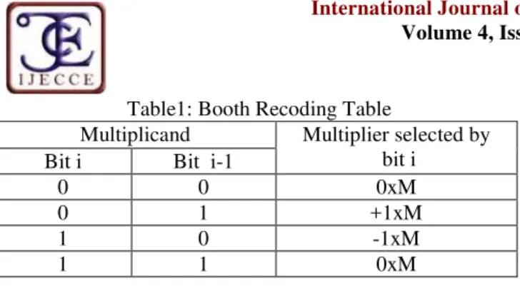
A. Booth Recoding Unit:
Copyright © 2013 IJECCE, All right reserved 1573
International Journal of Electronics Communication and Computer Engineering Volume 4, Issue 5, ISSN (Online): 2249–071X, ISSN (Print): 2278–4209
Table1: Booth Recoding Table
Multiplicand Multiplier selected by bit i
Bit i Bit i-1
0 0 0xM
0 1 +1xM
1 0 -1xM
1 1 0xM
B. Design of Column Bypass Multiplier
The column bypassing multiplier is constructed as follows. First, the modified HA cell is shown in figure. If aj = 0, the HA will be disabled. For a Braun multiplier, there are only two inputs for each FA in the first row (i.e., row 0). Therefore, when aj = 0, the two input of FA0,j are disabled, and thus it output carry bit will not be changed. Therefore, all three inputs of FA1,j are fixed, which prohibit its output from changing.
Fig.3. (a): Modified Full \Adder (b): Modified Half Adder Figure shows the 4x4 low power multiplier structure. This technique will be very useful as we go for higher width of the multiplicand specially when there are successive numbers of ones. If multiplicand contain at least one zero, it does not uses the Booth recoding unit and
if Multiplicand is “11” then only it will use Booth
recoding table shown in table . So we do not need sign bit circuitry. In this paper we have presented a new methodology for designing of low power parallel multiplier with reduced switching.
Fig.4. A 4x4 Column Bypass Multiplier
Method for increasing number of zeros in the multiplicand is discussed with the help of Booth Recoding Unit. Based on the modification of the half adders instead of full adders in an array multiplier, a low-power multiplier design column bypassing using Booth recoding is proposed. Compared with the row bypassing or array-multipliers, the experimental results show that our proposed low-power multiplier achieves higher power reduction with lower hardware overhead.
IV. E
XPERIMENTALR
ESULTSFor calculating performance of low power column bypass multiplier we have taken FIR filter as an application in which we used array multiplier and column bypass for MAC (multiply and accumulate unit) to examine the xpower calculation to prove how much the power can be reduced by this new multiplication method on sparten 2S30 FPGA and the design is synthesized on Xilinx 9.2i, synthesized results on Xilinx are shown below in table2, simulation results for the proposed design shown in figure5.
Table 2: Synthesis results using FIR filter on Xilinx
Characteristics Array
Multiplier
Proposed Design
Power dissipation 91mW 87mW
Estimated delay 7.89ns 5.20%
No of LUTs 31% 44%
Device Spartan 2 Spartan 2
Fig.5. Simulation results for the proposed design using FIR filter
V. C
ONCLUSIONCopyright © 2013 IJECCE, All right reserved 1574
International Journal of Electronics Communication and Computer Engineering Volume 4, Issue 5, ISSN (Online): 2249–071X, ISSN (Print): 2278–4209
R
EFERENCES[1] A. Wu, .High performance adder cell for low power pipelined multiplier., in Proc. IEEE Int. Symp. On Circuits and systems, May 1996,vol.4,pp.57-60.
[2] Hichem Belhadj, Behrooz Zahiri, Albert Tai .Power-sensitive design techniques on FPGA devices., Proceedings of international conference on IC Taipai(2003).
[3] Oscal T.-c.Chen, sandy Wang, and Yi-Wen Wu, .Minimization of Switching Activities of Partial Products for Designing Low-Power Multipliers, IEEE Transactions on VLSI systems, june 2003 vol.11,no.3.
[4] Rajendra M.Patrikar, K. Murali, Li Er Ping,. Thermal distribution calculations for block level placement in the embedded systems., Microelectronics Reliability44(2004) 129-134.
A
UTHOR’
SP
ROFILEV. Prakash
Pursuing final year M.Tech with the specialization of digital systems &computer electronics in the department of ECE in Malla Reddy Engineering College-Hyderabad, India. He completed his B.Tech in SIND Ramagundam. His interests are in VLSI and Embedded Systems.
Mekala Rama Rao
is working as an Assistant Professor in the department of ECE in Malla Reddy Engg College-Hyderabad, India. He is having 9 years of teaching experience in VLSI and Digital Electronics. His areas of interests are VLSI, Digital Electronics and Digital Signal Processing.