1
Mohammed Arifuddin Sohel,
2K. Chenna Kesava Reddy,
3Syed Abdul Sattar
1
ECED, Muffakham Jah College of Engineering and Technology, Hyderabad, A.P.
2
Principal, TKR College of Engineering, Meerpet, Hyderabad, A.P.
3Professor, ECED, Royal Institute of Technology and Sciences, Chevella, A.P.
A
BSTRACTA Low power discrete time sigma delta ADC consisting of a second order sigma delta modulator and third order Cascaded Integrated Comb (CIC) filter is proposed. The second order modulator is designed to work at a signal band of 20K Hz at an oversampling ratio of 64 with a sampling frequency of 2.56 MHz. It achieves a signal to noise ratio of 85.2dB and a resolution of 14 bits. The CIC digital filter is designed to implement a decimation factor of 64, operating at a maximum sampling frequency of 2.56 MHz. A second order sigma delta modulator is implemented in 0.18micron CMOS technology using full custom design and the third order digital CIC decimation filter is implemented in verilog HDL. The complete Sigma Delta ADC, consisting of analog block of second order modulator and digital block of decimator consumes a total power 1.96mW.
K
EYWORDSDiscrete Time Sigma Delta Modulation, Low Power design, Oversampling, CIC Decimation Filter
1.
I
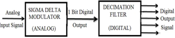
NTRODUCTIONAdvances in the integrated circuit (IC) technology have paved way for more compact and efficient implementation of digital logic on silicon. This indeed moved many types of signal processing to the digital domain. One of the major applications of this phenomenon is in data converters i.e., Analog-to-Digital converter (ADC) and Digital-to-Analog converter (DAC). Among the various Analog-to-Digital data, converters usually successive approximation or dual slope ADCs are used when high resolution is desired. But to achieve higher accuracy, trimming is required. The main constraint using these architectures is the design of high precision sample and hold circuits. The over sampling converters use digital signal processing techniques in place of complex and precise analog components, which, gives scope to achieve much higher resolution than the Nyquist rate converters. Sigma Delta ADC, a type of oversampling ADC is highly tolerant to analog circuit imperfections, thus making it a good choice to realize embedded ADC interfaces in modern systems-on-chip (SoCs)[1].
The sigma-delta ADC works on the principle of sigma-delta modulation. The sigma-delta ( )
input signal at an oversampling rate, generating a one bit output stream and decimator is a digital filter or down sampler where the actual digital signal processing is done. The decimator which is a crucial part of a sigma-delta ADC converts this one bit stream from modulator to a N bit stream according to resolution of ADC. This relaxes the requirement for high precision analog circuits required for the modulator stage and also increases the final output resolution of the ADC [2].
In the present paper, a modulator design in cadence analog environment and digital decimator design in verilog HDL in CADENCE mixed signal design environment is presented. The output of the modulator will be at the oversampling rate and its noise is shaped such that the signal is contaminated with quantization noise at higher (out of band) frequencies. This noise has to be filtered out using a digital filter.
There have been a number of approaches to realize low power Delta Sigma modulators [3]. In this paper, some low power optimization methods have been adopted in the design at both system and circuit level. A CIFB topology is used to design the system which ensures stable operation and low power consumption. A single-bit comparator and an advanced SC integrator topology based on Transmission Gates, which achieve high SNR is chosen.
The paper is organized as follows - Section II describes the basic principles of SD ADC and structure of first order modulator. In section III the Cascaded Integrator comb decimation filter basics are presented. In section IV, the detailed design of SD ADC is described, providing transistor level design and circuit simulations of OTA and other hardware components. The design results of the system and its sinusoidal response are also discussed in this section. The conclusion and future work is discussed in section VI.
2.
I
NTRODUCTION TOSD
ADC
Depending on the sampling rate, analog-to-digital converters are categorized into two types namely Nyquist rate converters and oversampling converters. Nyquist rate ADCs sample the
analog input at the Nyquist frequency, fn such that fs = fn = 2 x fb, where fs is the sampling
frequency and fb is the bandwidth of the input signal. Oversampling ADCs sample the analog
input at much higher frequencies than the Nyquist frequency. Sigma-delta ADCs come under this
category. In a sigma-delta ADC, the input signal is sampled at an oversampling frequency fs= K x
fn where K is defined as the oversampling ratio and is given by
K= fs /2fb (1)
Figure 1: Block Diagram of Sigma-Delta ADC
2.1. Quantization Noise
The analog input signal can take any continuous value. But a digital n-bit signal can only settle to
2n discrete values. It is this difference between the analog value and its digital representation,
which causes the distortion known as the quantization noise. Quantization error is defined as a measure of an n-bit converter’s failure to represent precisely an analog signal in the digital domain.
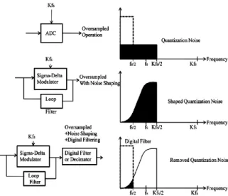
2.2. Oversampling, Noise shaping and Digital Filtering
Oversampling is a process of sampling the input signal at a frequency much greater than the
Nyquist frequency (Nyquist frequency, fn is defined as twice the input signal bandwidth, fb). This
process greatly reduces the quantization noise in the required band. The sampling theorem or the basic Nyquist sample theory states that the sampling frequency of a signal must be at least twice the input signal frequency in order to reconstruct the sampled signal without distortion. Figure
2(a) shows the spectrum of an under sampled signal [8]. Here the sampling frequency, fs is less
than twice the input signal frequency 2fo. The shaded portion of the figure shows the aliasing
which occurs when the sampling theorem is not followed. We get a distorted signal at the output when a signal contaminated with aliasing is recovered. Figure 2(b) shows the spectrum of an oversampled signal [4]. Here the sampled signal in the frequency domain appears as a series of band-limited signals at multiples of sampling frequency that are widely spaced. This process puts
the entire input bandwidth at less than fs/2 which reduces the aliasing.
Figure 2(a): Under sampled signal 2(b) Oversampled signal spectrum
Noise shaping is a property of sigma-delta ADCs resulting from the application of feedback that extends dynamic range. A closed loop modulator works as a high-pass filter for quantization-noise and as a low-pass filter for the input signal. When the signal is oversampled, the
quantization noise power in the Nyquist bandwidth (fs/2) spreads over the wider bandwidth, Kfs/2
where; K is the oversampling ratio, which is shown in Figure 3.The total quantization noise is still the same but the quantization noise in the bandwidth of interest is greatly reduced. The figure also illustrates the noise shaping achieved by using the oversampled sigma-delta modulator.
Figure 3: Effect of Noise shaping and Digital Filtering
The SQNR of a Nyquist Rate convertor in equation 2 is compared with that of an ‘oversampling only’ modulator in equation 3 which shows the marked increase in SQNR by a factor of 10 Log(K). It is kept between 16-512 times the Nyquist rate. In order to further increase the SQNR,
an L th order noise shaping is performed that leads to increase in SQNR by a factor of 10(2L+1)
Log (K) as seen in equation 4[6].
SQNR= 6.02N + 1.76 dB (2)
SQNR = 6.02N + 10 Log (K) +1.76 dB (3)
SQNR = 6.02N + 10(2L+1) Log (K) +1.76 dB (4)
The block diagram of a first order sigma-delta modulator is shown in Figure 4 where the quantizer is modeled as a source of additive noise.
Figure 4. First Order Sigma Delta Modulator
The output (V) of first order modulator in terms of input(U) and additive noise(E) is given in equation 5. The signal transfer function (STF) and Noise Transfer Function (NTF) are given by equation 6 and 7 respectively,
V=STF. U + NTF. (5)
STF = V(z) /U(z) = Z-1 (6)
The signal appears unchanged at the output with just a delay whereas the noise is subjected to
first order differentiation such that it is pushed out of signal band. The NTF of an L th order
modulator will get modified as shown in equation 8[7].
NTF(z) =(1- Z-1)- (8)
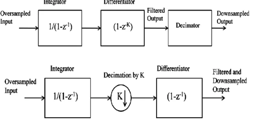
3. Cascaded Integrator Comb (CIC) Decimation Filter
The CIC filter is a multiplier free filter that can handle large rate changes. It was proposed by Eugene Hogenauer in 1981 [8]. It is formed by integrating basic 1-bit integrators and 1-bit differentiators. It uses limited storage as it can be constructed using just adders and delay elements. The CIC filter can also be implemented very efficiently in hardware due to its symmetric structure. The transfer function of the CIC filter in z-domain is given in equation 9.
(9)
In equation 9, K is the oversampling ratio and L is the order of the filter. The numerator (1-z-K)L
represents the transfer function of a differentiator and the denominator 1/(1-z-1)L indicates the
transfer function of an integrator.
The CIC filter first performs the averaging operation then follows it with the decimation. A simple block diagram of a first order CIC filter is shown in Figure 5. In Figure 5(a), the differentiator circuit needs K (oversampling ratio) delay elements, which are implemented using registers. The number of delay elements increases as oversampling ratio increases, and as well the number of registers bits that are used to store the data. This type of implementation becomes complex and requires more area as we go for higher order and higher sampling rates. This problem can be overcome by implementing a decimation stage between the integrator and differentiator stages as shown in Figure 5(b). Here the clock divider circuit divides the oversampling clock signal by the oversampling ratio, K after the integrator stage. The same output can be achieved by having the decimation stage between integrator stage and comb stage. By dividing the clock frequency by K the delay buffer depth requirement of the comb section is
reduced. In Figure 5(b), the integrator operates at the sampling clock frequency, fs while the
differentiator operates at down sampled clock frequency of fs/K[9]. By operating the
differentiator at lower frequencies, a reduction in the power consumption is achieved.
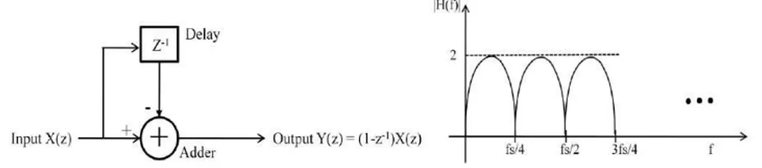
3.1 First Order Digital Integrator
The integrator consists of a delay element and a full adder. A simple register can be used to achieve the delay. The magnitude response plot of the integrator is as shown in Figure 6. It is
basically a low-pass filter with a -20 dB per decade roll off and infinite gain at dc and fs.
Figure 6: Block Diagram and Magnitude Response of first order Integrator
A single integrator is unstable due to the single pole at z=1. There is a chance of register overflow and data may be lost. To avoid this problem with register overflow, 2's complement coding scheme is used. By using the 2’s complement number representation, the data will not be lost due to register overflow as long as the register used to store the data is long enough to store the
largest word given by Kx2N. Here N is the number of input bits to that particular integrator stage.
Internal word width (W) needed to ensure no run time overflow is estimated from equation 10 [10].
W = (1Sign bit) + (Number of input bits) + (Number of stages, N) log2(Decimator factor) (10)
In this paper, W = 1 + 1 + 3 log2(64) i.e. W=20
3.2 First Order Digital Differentiator
The differentiator also known as comb filter is an odd symmetric FIR filter. The block diagram and magnitude response are shown in figure 7. It is basically a high-pass function with a 20 dB per decade gain. The 2’s complement output of the integrator is applied as the input to the differentiator. Hence the differentiator also uses the 2’s complement scheme of coding. So the output at the end of the differentiator will be in 2’s complement form and has to be converted back to binary form.
Fig 7: Block Diagram and Magnitude Response of first order Differentiator
A CIC decimation filter is a cascade of an integrator followed by a a differentiator, each integrator contributes a pole to the CIC transfer function while each comb section contributes a zero of order K[11], where K is the frequency decimation ratio and N is the order of the decimation filter. The total response of a CIC filter at frequency, fs is given by equation (11).
Equation (11) implies the equivalent time domain impulse response of a CIC filter. It can be viewed as a cascade of N rectangular pulses. Each rectangular pulse has KM taps. Equation (12) gives the magnitude response of a CIC filter at frequency, f where N is the order of the filter.
(12)
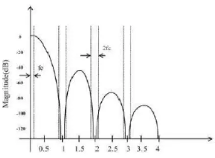
The frequency response of the CIC filter obtained using equation (12) is shown in figure 8. The
figure shows the aliasing bands 2fc centered around multiples of the sampling rate. As the number
of stages in a CIC filter is increased, the frequency response has a smaller flat pass band [11].
Figure 8: Frequency response of a CIC filter
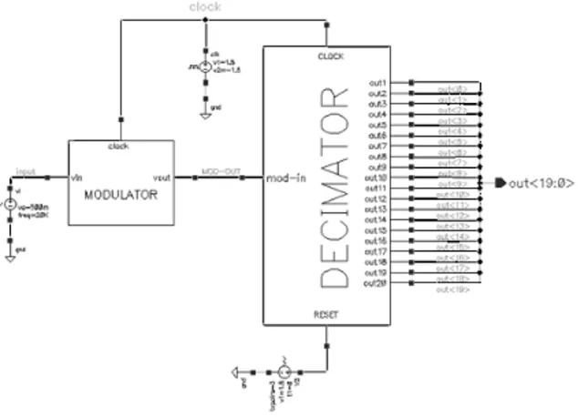
4. System level Design of Sigma Delta ADC
The Sigma Delta ADC (SDADC) as shown in figure 1 consists of a sigma delta modulator followed by a Decimation Filter. In this paper, a 14 bit DT-DSM for audio band frequencies is implemented in 180 nm CMOS technology. The modulator runs on a 1.8 V supply and achieves a SQNR of 85.2 dB for a signal bandwidth of 20 KHz. The modulator operates with an oversampling ratio (K) of 64 and a sampling frequency of 2.56 MHz. The decimation filter accepts the single bit stream from the modulator and converts it into a 14 bit digital output.
4.1 Design of Second Order Sigma Delta Modulator
The various steps involved in the process of design of modulator include using the order, OSR and modulator topology (CIFB in this case) to generate the Noise Transfer Function. Richard Schrier’s toolbox [5] is a very efficient tool to extract the loop filter coefficients which are given in Table 1.
Table 1: Loop filter Coefficients
a1 a2 b1 c1 c2
0.2112 0.1334 0.2112 0.1763 5.8163
Figure 9: Simulink Model of second order Sigma Delta Modulator
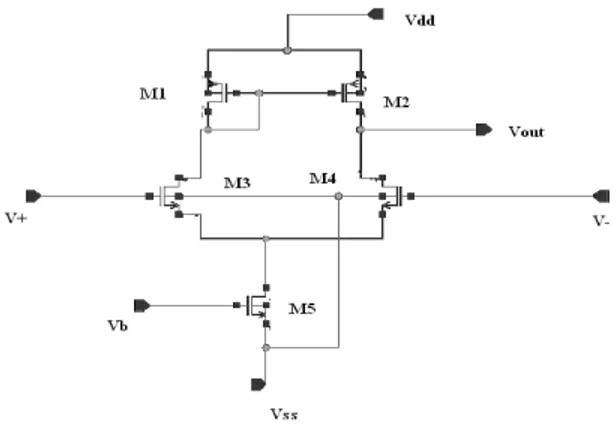
4.1.1 Design of Basic CMOS OTA:
The basic building block of all these modules is the Operational Transconductance Amplifier (OTA). The transistor version of the Basic CMOS OTA is shown in the figure 10[12]. The OTA designed achieves a gain 33.57 dB and phase margin of 75 degrees for a capacitive load of 1 fF. It operates at a unity gain frequency (UGB) of 8 GHz.
Figure 10:Transistor version of Basic CMOS Operational Transconductance Amplifier (OTA)
4.1.2 Comparator and DAC
A comparator is a device which compares two voltages or currents and switches its output to indicate which is larger. The transistor version of the CMOS comparator implemented with PMOS input drivers and input biasing resistor is as shown in figure 11. The bias resistor was chosen to be 250 ohms and a capacitive load of 43 femto farads was provided.
4.1.3 Complete Design of second order Switch Capacitor Sigma Delta Modulator
The complete transistor level design of second order Switch capacitor Sigma Delta modulator is done by carefully choosing the values of capacitors to implement the coefficient values obtained in table 1 earlier. The switch is implemented using transmission gate logic for the obvious reason that both logic 1 and logic 0 can be conducted without any loss of logic level. A special function called filewrite.v is written in verilog that extracts the bit stream from cadence environment. This bit stream is then exported to matlab and the calculation of SNR and ENOB is performed.
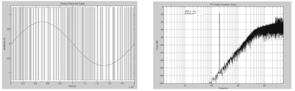
The transient response of second order SDM for a sine wave input of 20 K Hz with a clock frequency of 2.56 M Hz at an OSR of 64 is shown in figure 12(a). It is clearly evident that the output (single bit) is pulse width modulated according to the input sine wave. The number of 1’s increases at the positive peak of the input sine wave and the no of 0’s are more at the negative peak. There are equal number of 1’s and 0’s when the input signal is at zero amplitude, which is the expected response of a Sigma Delta Modulator.
Figure12(b) shows the power spectral density (PSD) of the switched-capacitor circuit implementation of the proposed Delta Sigma modulator for the input sine wave of frequency of 20kHz. The sampling frequency is 2.56MHz. A 65,536 point Blackman Harris Window is used for PSD computations The SNR of 84dB giving a resolution or ENOB of 14 bits is achieved. The modulator dissipates 2.35mW for a 1.8V supply.
Figure 12 (a): Transient response of second order SDM for a sine wave input of 20 K Hz (b) Power Spectral Density (PSD) of output of SDM
4.2 Design of Third Order Digital Decimation Filter.
The block diagram of the decimator designed in this work is shown in Figure 13. The input to the decimator is a 1-bit pulse density modulated signal from a second order sigma-delta modulator .The output from the decimator is a 20 bit digital output. The different blocks were designed to be implemented in 180nm CMOS technology. The hardware required to build each block was designed using Verilog HDL in Cadence and then the schematic of different blocks was created from the Verilog code in Cadence Virtuoso.
4.2.1Coder Circuit
The purpose of the coder circuit is to increase the resolution of the ADC. The output from the second order modulator is one bit binary, i.e. it is either 1 or 0. A register overflow might occur at
the multiples of fs due the infinite gain. This register overflow can be avoided if the register
length of the integrator is chosen according to equation (10) and also by using the 2’s complement method of coding. The two outputs of the coder circuit for binary 1 and 0 inputs are shown in Table 2.
Table 2: 20 bit Output of Coder circuit
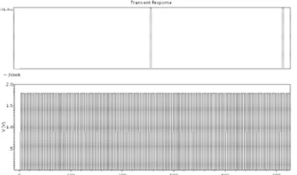
4.2.2 Clock Divider Circuit
The function of the clock divider circuit is to divide the clock frequency by the oversampling
ratio, K=64. The input to the clock divider circuit is the oversampling clock, fs, which is also used
as the clock for the modulator. Hence, the output of the clock divider is fs/64 and is applied to the
differentiator circuit of the CIC filter [14]. The clock divider circuit is designed using negative edge triggered T-flip flops and AND logic gates.
Figure 14: Oversampling clock input and divide by 64 output
4.2.3 Delay Element
A delay element is a register circuit, which is used to provide a delay by one clock period. The
integrator and differentiator circuits of a 3rd order CIC filter requires 120 delay elements. The
integrator block alone requires 60 delay elements, 20 for each stage. The differentiator block requires 60 delay elements, which are divided equally between the three differentiator stages. Hence it is very important to design a delay element which is area efficient and has smaller rise and fall times. A delay element can be implemented using a combination of switches and inverters.
4.2.4 20-bit Down Sampling Register
The 20-bit output from the differentiator stages has a continuous differentiated output .We need
the output of the differentiator at the instances where the clock divider output (fs/64) is high. This
only after this initial no-valid output time period has elapsed which would be 3KTs seconds [15].
For the second order over sampled sigma-delta modulator and the third order CIC filter used in
the design, the desired output resolution is given by the equation (13).
(13)
In equation (13), Ninc is the increase in resolution and K is the over sampling ratio. So, for K=64,
the output resolution achieved is 14 bits. Hence, we select 15-Bits (1-sign bit +14 resolution bits) from the 20-bit output of the differentiator and drop the lower 5 bits. Bit 19 or MSB is taken as sign bit and bit 18 to bit 5 (14-bits) are considered to calculate the discrete value of the output.
4.3 Complete System Design of SD ADC
The 1-bit ± 1.8V output from the modulator is applied to the input of the CIC filter. The built-in coder circuit boosts the resolution from 1-bit to a higher resolution of 20-bit. The 20-bit 2's complement input is then applied to the 3rd order integrator. The output from integrator stages is then applied to the 3rd order differentiator stage. Each differentiator stage output is passed through the down sampling registers. The output of the differentiator, which is also the output of the decimator, is the final output of the sigma-delta analog-to-digital converter. The test setup for the sigma delta ADC is as shown Figure 15.
Figure 15: Test setup for sigma delta ADC
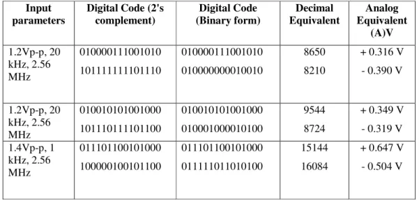
The output of the CIC filter is in 2's complement form occurring at twice the input signal bandwidth. As discussed earlier the desired 15 bit output is converted from 2’s complement to equivalent binary form. The applied sine wave input to the ADC is 1.2Vp-p, 20 kHz with a bandwidth of 40 kHz and the applied over sampling clock frequency is 2.56 MHz and hence the output occurs at 40 kHz. For an ADC 1 LSB is defined as in equation 14
(14)
In equation (14), VFSR is the full-scale voltage range of the input signal and N is the number of
output bits. In this particular case VFSR for positive half cycle of the sine wave is 0.6V and
number of bits, N=14. The experimental results are illustrated in Table 5.1, which shows the 15-bit 2's complement output, binary output, its decimal equivalent, and the actual analog voltage. In Table 5.1 a set of 3 data samples are shown together. Based on the equation (14), for the case of
LSB value is used in finding the analog equivalent of the digital output. The decimal equivalent value for the first data stream is obtained as shown below:
1*213+ 0*212 + 0*211 + 0*210 + 0*29 + 1*28 +1*27 + 1*26 + 0*25 + 0*24 + 1*23 + 0*22 + 1*21 + 0*20 = 8650.
The actual analog value of the decimal equivalent is obtained by multiplying the decimal equivalent value with the value for 1 LSB. For the decimal value of 8650, its analog equivalent is given by 8650 x 0.0366 mV = 0.316V. The experimental output results calculated for 1 cycle of sine wave input are given in Table 3.
Table 3: Tabular Data Representation of the 14-bit decimator output for K = 64 case
Input parameters
Digital Code (2's complement) Digital Code (Binary form) Decimal Equivalent Analog Equivalent (A)V 1.2Vp-p, 20 kHz, 2.56 MHz 010000111001010 101111111101110 010000111001010 010000000010010 8650 8210
+ 0.316 V
- 0.390 V
1.2Vp-p, 20 kHz, 2.56 MHz 010010101001000 101110111101100 010010101001000 010001000010100 9544 8724
+ 0.349 V
- 0.319 V
1.4Vp-p, 1 kHz, 2.56 MHz 011101100101000 100000100101100 011101100101000 011111011010100 15144 16084
+ 0.647 V
- 0.504 V
The power consumed by second order modulator is 1.622mW and by the digital decimation filter is 238 micro watts. Hence, the complete ADC consumes a power of 1.96 mW which is a very low power consumption when compared to current state of art converters.
5. Conclusion.
R
EFERENCES[1] José M. de la Rosa, “Sigma-Delta Modulators: Tutorial Overview, Design Guide, and State-of-the-Art Survey” IEEE Transactions on Circuits and Systems—I: Regular Papers, vol. 58, No. 1, January 2011.
[2] Mohammed Arifuddin Sohel, Dr. K. Chennakeshava Reddy and Dr. Syed Abdul Sattar, “A 12 Bit Third Order Continuous Time Low Pass Sigma Delta Modulator for Audio Applications”, International Journal of Electronics and Communication Technology (IJECT), vol. II, Issue 4, page(s): 211-216, October 2011.
[3] Ovidiu Bajdechi, Johan H.Huijsing, and Georges Gielen, "Power Optimization in SD ADC Design," Proc. International Conference on Digital Signal Processing, IEEE Press, 2002, pp. 353-359, doi: 10.1109/ICDSP.2002.1027902.
[4] S. Pavan and Nagendra K, “Tutorial on Sigma Delta ADC”, VLSI Conference, 2008, Hyderabad, India.
[5] R. Schreier and G. C.Temes, IEEE Press “Understanding Delta-Sigma Data Converters”, A John Wiley and Sons publication, 2003.
[6] V. Peluso, M. Steyaert, and W. Sansen, Design of Low-Voltage Low-Power CMOS Delta-Sigma A/D Converters. Norwell, MA: Kluwer, 1999.
[7] Behzad Razavi, “Design of Analog CMOS Integrated Circuits”, Tata McGraw Hill, Edition 2002. [8] E. B. Hogenauer, “An economical class of digital filters for decimation and interpolation,” IEEE
Transactions on Acoustics, Speech and Signal Processing, Vol. 29, pp.155-162, 1981.
[9] A. Srivastava, R. R. Anantha, “A programmable oversampling sigma-delta analog-to-digital Converter,” IEEE proceedings of Midwest Symposium on Circuits and Systems, Vol. 1,pp.539-542, August 2005.
[10] K. F. Chong, P. K. Gopalakrishnan, T. H. Teo, "Low power approach for decimation filter hardware realization,” Proceedings of World Academy of Science, Engineering and Technology, Vol. 32, pp. 2070-3740, August 2008.
[11] Altera Corporation, “Understanding CIC compensation filters,” Application Note 455, Ver.1.0, April 2007.
[12] D. A. Johns and K. Martin, “Analog Integrated Circuit Design”, John Wiley & Sons, New York, New York, 1997.
[13] Dr. Hsu Kuan Chun Issac, “A 70 MHz CMOS Band-pass Sigma-Delta Analog-to-Digital Converter for Wireless Receivers”, A Ph.D thesis submitted to The Hong Kong University of Science and Technology.
[14] G. Stephen, R. W. Stewart, "Sharpening of partially non-recursive CIC decimation filters," Asilomar Conference on Signals Systems and Computers, Vol. 2, pp. 2170-2173, November 2004.
Authors
1.Mr. Mohammed Arifuddin Sohel is working as Associate Professor in Electronics and
Communication Engineering Department of Muffakham Jah College of Engineering and Technology, Hyderabad. He Completed his B.E (ECE) from Osmania University in 2001 and M.E in Microelectronics Engineering from RMIT University, Melbourne, Australia in 2004. He is currently pursuing Ph.D in VLSI Design from JNTU, Hyderabad in the area of Analog and Mixed Signal VLSI Design. He has 10 years of teaching Experience and has published a few papers in international and national conferences and Journals. He is a member of IEEE and life member of IETE. He is also serving as the Treasurer of
Joint Chapter of IEEE Circuits and Systems and Electron Devices (CAS/EDS) of IEEE Hyderabad Section. 2. Dr.K. Chenna Kesava Reddy received the B.E degree, M.Tech degree from
Regional Engineering College (REC), Warangal in 1973 and 1976 respectively, PhD from JNT University, Hyderabad in 2001. He served on the Department of Electrical Engineering, REC Warangal for 1.5years as Research Associate in Problem Oriented Research Lab (P.O.R.L). He was with JNTU, Ananthapur from 1977 to1979. He served in the Dept of ECE, JNTU Hyderabad from 1979 to 2001 at various levels. From December 2001 to September 2006, he was the Deputy Director of UGC Academic Staff College, JNTU Hyderabad. He worked as Director of Evaluation at JNTU Hyderabad from 2006 to 2007. Dr. Chenna Kesava Reddy was Principal of
JNTU College of Engineering, Jagityal, Karimnagar from May 2007 to June 2009. Presently, he is working as professor and principal at TKR Engineering College, Hyderabad. He has published 70 research papers at National and International levels.
3. Dr. Syed Abdul Sattar, is presently working as a Dean of Academics & Professor of ECE department, RITS, Chevella, Hyderabad. He has completed his B.E. in ECE in 1990 from Marathwada University, Aurangabad, M. Tech. in DSCE from JNTU Hyderabad, in 2002, and did his first Ph.D. from Golden state University USA, with Computer Science in 2004, and second Ph.D. from JNTU Hyderabad, A. P. India with ECE in 2007. His area of specialization is wireless communications and image Processing. He has about 21years of experience in teaching and industry together and recipient of national award as an Engineering Scientist of the year 2006 by NESA