A SPICE compatible Model for Intel
®’s 45nm High
MOSFET
A. Ávila¹, D. Espejo².
!" # $ % &
' (' ' ! '
& ) *!+,
,
' - ./ 0 $ - ! ,
' 0 ' - '
0 !" # $ 0 % $ 1
' - 0
2' 3
/ ' 4
' 0 0
4 % , 4
2' 0 5 % $
- 4 0 678 2'
4 %
! "# $% & ' I. INTRODUCTION
As semiconductor industry is looking for increasing levels of circuit integration and fulfilling of Moore's Law [1], the discipline of semiconductor devices modeling is facing challenges arising from scaling. Intel ™ has proposed [2] a new insulating material for MOSFET’s dielectric: , whose dielectric constant , nearly 4 times that of traditional SiO2, provides the advantage of reducing the probability of the occurrence of leakage currents caused by effects such as tunneling, which are more likely to happen in short channel devices. This article describes the procedure developed in order to build a model compatible with SPICE ™ for Intel®’s MOSFET, and that can be used for single gate MOSFETs with as gate dielectric. This model describes device behavior by consideringthe effects associated with short ( ) and increasing , with accuracy over 98% compared with Intel®’s data [2].
II. MOSFET ARCHITECTURES STATE OF THE ART As a first step, different architectures of current MOSFETs were identified, from 2005 onwards, both in research and production stages, in order to acknowledge their main parameters and size, comparing them under the same parameter: . The results of this stage are summarized in Table 1, which has been ordered by from lowest to highest
Manuscript received June 01, 2011; revised June 29, 2011.
¹A. Ávila is an associate professor at the Department of Electrical and Electronics Engineering, University of the Andes (Universidad de los Andes), Carrera 1 Este # 19A 40, Mario Laserna building, ML 320 office, Bogotá, Colombia (Phone: (+571) 339 4949, extension 2828; fax: (+571) 339 4949; e mail: a [email protected]).
²D. Espejo is pursuing his Master’s degree at the Department of Electrical and Electronics Engineering, University of the Andes (Universidad de los Andes), Carrera 1 Este # 19A 40, Mario Laserna building, ML 008 office, Bogotá, Colombia. (e mail: [email protected]).
TABLE I NOVEL MOSFET STRUCTURES
9 0 # # $ : 5;: $ :
R R P R P
* ) + 20 30 45 50 60
9 Si
segment divides the Gate
Gate material surrounds
channel
High k gate dielectric
controlled through a deposited film thickness
Three effective gates, sources and drains
9 4 )<+
44n 30n 61n 39µ 72µ
R: Research P: Production
Taking into account that, at the time of this stage of research, Intel’s 45nm High k MOSFET, was the one with the world’s smallest in production (being passed in January 2010, following the launch of Core processor 32 nm family [3]), authors chose to describe and achieve a model for this device to provide a considerable relevance to the results of this research.
III. INTEL’S MOSFET ELECTRICAL AND PHYSICAL PARAMETERS
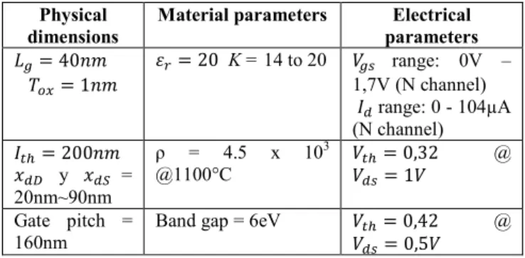
After the review of the available literature about the studied device, the physical (mainly, material properties) and electrical parameters reported by the manufacturer were gathered [2]:
TABLE II
Intel 45nm MOSFET ELECTRICAL AND PHYSICAL PARAMETERS
- !
= 40
= 1 = 20 14 to 20 1,7V (N channel) range: 0V –
! range: 0 104µA (N channel)
"#= 200
$!% y $!& = 20nm~90nm
ρ = 4.5 x 10³
@1100°C "#= 0,32
@
! = 1
Gate pitch = 160nm
Band gap = 6eV "#= 0,42 @
! = 0,5
From the above data it is possible to recognize that in this device, T+, has the dimension of a few atomic layers and the insulator material is about 4 times more resistant to carrier tunneling, compared with the traditional SiO , which is equal to 3,9. The studied device is considered as a
, because its is in the same order of magnitude as $!% and $!& , which sets up a scenario where the electric field in the direction perpendicular to the semiconductor oxide interface is high with a tendency to keep growing, and where the phenomena known as Proceedings of the World Congress on Engineering and Computer Science 2011 Vol II
WCECS 2011, October 19-21, 2011, San Francisco, USA
ISBN: 978-988-19251-7-6
ISSN: 2078-0958 (Print); ISSN: 2078-0966 (Online)
is most likely to occur. One of the research questions that motivated the work documented here has to do with the presence or absence of such effects in MOSFET models available in SPICE based simulators. An observation of models developed by the University of California, Berkeley and other schools and companies such as Phillips Semiconductor, shows that the models still fail to accurately describe the behavior of short channel MOSFETs. That is the case of the latest MOSFET model developed for SPICE: BSIM 4.6.4. Its manual [4], indicates that its 0122 designed limit is 1nm, however, to model devices with high k dielectric, proposes a simple proportions relationship to calculate equivalent EOT from the one of devices with SiO as dielectric. An approach as simplistic as this one, may lead to high inaccuracy in the description of device behavior. These limitations present in the latest MOSFET model developed for SPICE, led to the need for a new device model to be tested with Intel´s 45nm MOSFET physical and electrical parameters.
IV. AMODEL FOR CARRIER QUANTIZATION Given that in Intel’s 45nm MOSFET, carrier tunneling through the dielectric is considered more likely to happen, and that under that phenomena, carriers behave in a way similar to waves, also being confined in a potential well by a high 34; it is necessary to model the behavior of the device through a description of the carrier as particle as well as wave. The proposed procedure starts from Poisson equation describing 2 D potential distribution 5(6, 78 along the channel:
9:;(,,48 9,: <
9:;(,,48 94: =
=
>?@(AB(68 < C(6, 788 (1)
In the scenario in which the charge is quantized, the continuous conduction band is now divided into two sub bands. The wave function of each sub band is given by the Schrodinger equation:
#:
DE:F G HI($, J8FK($, J8 = KFK($, J8 (28
Noting that carriers confinement is higher in the direction perpendicular to the Gate, the one dimensional Schrodinger equation is enough for the problem. By ensuring a MOS structure with uniform potential distribution along the direction perpendicular to the Gate, variable can be removed from Poisson's equation, and reduce the problem to coupled one dimensional equations of Schrodinger Poisson:
!:L( 8 ! : =
MNO( 8 PQR G S
TRUV,R
MPQR WFK($8W:
K (3)
G#DX!X!Y( 8X G HI($8F($8 = F($8 (48
Reaching an analytical solution for this pair of equations is not an easy task; however, numerical simulations provide some insights into reaching this solution.
Figure 1 shows the results of simulating the carriers population per sub band, using the parameters of Intel®'s High K MOSFET: Z!= 1[\] ^, = 1 y = 22:
Figure 1. Numeric simulation of carrier populations per sub band, simulation conduced using SCHRED [5] with parameters Tox = 1nm, T = 300°K and Nd = 10[\] _`.
From Fig. 1, as we move amid 0V<abc<3V, it is possible to see that between 45% and 85% of the carriers reside in the lower sub band, so only the lowest level of energy will be considered to approach to the analytical solution. With that estimate, the pair of equations (3) and (4) for each valley or group of sub bands associated with the crystal structure of the interface are reduced to:
!:L( 8 ! : =
MNO( 8 PQR <
TRUV,d
MPQR eF[,[($8e: < TRUV,X
MPQR eF[, ($8e: (58 G #DXR!Xfd,d! X( 8G HI($8F[,K($8 = K,[FK,[($8 i=1,2(68
Where denotes each of the two valleys where the lowest energy level will be obtained.
!
Using calculus of variations, wave functions are assumed with shape similar to h[,[ y h[, , thereby ensuring a good level of accuracy for the calculated energy levels [6]. Now we proceed to integrate the simplified Poisson equation from the bulk to the surface. And in order to find the lowest expression of energy, expected value of the wave function h[,[ Hamiltonian is calculated obtaining the following
expression:
[,[= i F[,[($8
X
Dd !
! XF[,[($8j$ < i HI($8lk
k
l F[,[($8:j$
(7)
With the simulation of the sub bands wave functions, we can get closer to the analytical solution:
Proceedings of the World Congress on Engineering and Computer Science 2011 Vol II WCECS 2011, October 19-21, 2011, San Francisco, USA
ISBN: 978-988-19251-7-6
ISSN: 2078-0958 (Print); ISSN: 2078-0966 (Online)
(14) Figure 2. Sub bands wavefunctions, simulation conduced on SCHRED [5].
Simulation of Fig. 2 shows that the peak of carrier density is a few nanometers (no more than 5 nm) below the channel surface, which leads to approximate:
j mn[d and j mn[
X, (8)
Then, this approximation is applied and the result is factorized, based on the parameter γ of proportionality. According to the variation method, o[ and o should minimize the energy level, ie:
!pd,d
!nd = 0 and
!pd,X
!nX = 0 (9)
Calculating the derivatives, we obtain the expressions for o[ and o , then the mean value of γ is obtained. Finally, replacing the values obtained and the approximations described above, leads to the expressions for 3[,[ and 3[, :
[,[=`#:nDdd: y [, =`#:nDX:
X q 1,432 [,[ (10)
Verification of model validity is done by comparing its results with SCHRED simulation of energy levels for sub bands:
Figure 3. Energy levels at each valley, by model expressions and by SCHRED simulation
Accuracy of the quantization model obtained, allows us to approach a short channel I V model that takes into account the quantization of charge that occurs at this scale, and enables some approximations for that model, keeping the same accuracy.
V. I VSHORT CHANNEL MODEL
The fact that, in short channel devices, there is no complete control of the channel charge is an indicator that 34 is not negligible compared to 3, and the effects associated with this fact should be incorporated in a compact model. In terms of rs, the most significant effect to be included is
, that may result in reduced effective saturation rs.
!
One of the empirical relations in use to model the dependence of carrier velocity tswith respect to 3, was adopted for this step [7]:
Wu!W =Wvw[|WpWxyzzWpW/WpzW/Wp{W{W (11)
The first expression to find is the one for rs in linear region r}~•. 3, is expressed as the differentials of the potential
between the polarization of the inversion layer and the end of the piece. Integrating these differences along the channel, we obtain the rs expression at non saturation regime:
%&=€•‚ƒ „(…†Q_…‡ˆ8…‰Q_lŠ‹n…‰Q X
[|Œ‰Q•Ž• • %&‘ ’%& (12)
For the expression in the saturation region, it is necessary to
include the effect of " ! or CLM
[6], finding the value of asc in which saturation occurs, so the expression of rsc in presence of velocity saturation is given by:
r}~= “”•+,–—˜™?-˜›œ˜’•?-lŠ‹ž˜•?
X
Ÿ [-¡¢£|¤’•?£¥¦§ ¨ (13)
# $% !
Finally, to obtain a unified expression of rs in presence of velocity saturation, it becomes necessary to incorporate the smoothing equation of ! :
!©ªª= %&«¬G12 - %&«¬G %&G ® < ¯( %&«¬G %&G ® 8 < 4® %&«¬
Thus, as122 is used to replace asc in the ! expression, as well as the effective voltage aB122 to incorporate CLM in the unified expression, that is then obtained:
! =[|—³´w°°w±²²w±²²œ/…w±²² (14) with
!©ªª= 1 <…‰Q…_…O±²²w±²²§ ! l y «©ªª=pQO‡•±²²(pQO‡•±²²|…‰Q8
µ…w±²²
(15)
Proceedings of the World Congress on Engineering and Computer Science 2011 Vol II WCECS 2011, October 19-21, 2011, San Francisco, USA
ISBN: 978-988-19251-7-6
ISSN: 2078-0958 (Print); ISSN: 2078-0966 (Online)
! & $% ' ! ( )
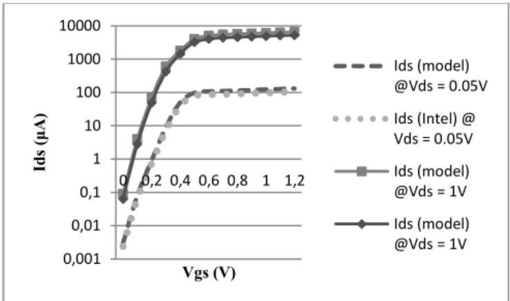
With the physical and electrical parameters given in Table 2
and those obtained by the * +
, - ! for 45 nm node [8], we
compare the results using the IV model expressions obtained from the curve provided by the manufacturer [2]:
Figure 4. I V characteristic by model expressions and Intel®’s data
The results show a correlation coefficient R² equal to 0,9 and an average error of 0.33, indicating a relatively strong relationship between the data obtained by the model and those reported by the manufacturer. This level of accuracy, allows us to get to the next stage, which is the model equations testing in SPICE.
VI. TESTINGTHEMODELEXPRESSIONSINA
SPICECIRCUIT
To ensure the portability of the model for any SPICE based simulator, obtained model expressions were incorporated using Analog Behavioral Modeling blocks, included in Orcad© PSPICE 9.1. Those blocks have a maximum of three inputs and one output of voltage or current. They use mathematical relationships to model a circuit segment and, when connected in cascade, and at generation stage, the simulator concatenates the blocks to make the entire expression. Expressions are entered in the model and tested in a configuration of half wave rectifier inverter, compared with an N channel MOSFET in the same configuration, whose electrical and physical parameters have been replaced by the ones of Intel’s MOSFET to verify the performance of BSIM4 model at sub 50nm scale and the operation of the model obtained in a circuital implementation. Simulation shows us the degradation in the description of the MOSFET in sub threshold regime by BSIM4 model and a good performance of model expressions obtained.
Figure 5. Transient analysis using Orcad PSICE™ 9.1 for three signals: 1 – Output voltage of native N MOS MOSFET with High k transistor physical and electrical parameters running under BSIM 4.4 model, 2 – output of ABM blocks running model expressions obtained with this methodology, 3 – input voltage signal with amplitude of 5V and 60 Hz frequency. This results show that current MOSFET compact models like Berkeley’s BSIM cannot simulate device behavior properly at the nano scale because the lack of a Quantum mechanical approach, and show good performance of model expressions in a common circuit configuration.
CONCLUSIONSANDRECOMMENDATIONS
A novel modeling methodology, based on the effects of charge quantization on device behavior has been developed, obtaining a compact model that describes, with accuracy over 98%, the behavior of the Intel™’s 45nm MOSFET in the presence of velocity saturation and "# shift. The proposed methodology has been condensed into a learning object SCORM compatible (Sharable Content Object Reference Model), which is available at
% .// / /01123. Future work could
include additional effects such as temperature dependence and body effect among others. The model could be simplified to have as few parameters as possible, avoiding a great number of ABM blocks.
REFERENCES
[1] G. Moore, “Cramming more components onto integrated circuits,” Electronics, vol. 38, No. 8. 1965
[2] K. Mistry, C. Allen, C. Auth., “A 45 nm logic technology with High k metal gate transistors, strained silicon, 9 Cu interconnect layers, 193nm dry patterning and 100% free Pb packaging”, IEDM, 2007. [3] Intel, “Technology at Intel:January 2010 Archive”. Available on
http://blogs.intel.com/technology/2010/01/ retrieved on 11/17/10 [4] T. Morshed, et. al., “BSIM 4.6.4 MOSFET Model: User’s Manual”,
University of California, Berkeley, 2009.
[5] D. Vasileska, S. Ahmed, M. Mannino, A. Matsudaira, G. Klimeck, M. Lundstrom, & ), available on
http://nanohub.org/resources/schred
[6] L. Wang, “Quantum mechanical effects on MOSFET scaling limit”, thessis for the PhD degree, School of Electrical and Computer Engineering, Georgia Institute of Technology, 2006.
[7] Z. Ren, “Nanoscale MOSFETs: Physics, simulation and design”, thessis for the PhD degree, Purdue University, 2001.
[8] University of California, Berkeley, Arizona State University, Berkeley Predictive Technology Model, available on
http://ptm.asu.edu/modelcard/LP/45nm_LP.pm, retrieved on 26/04/10 0,001
0,01 0,1 1 10 100 1000 10000
0 0,2 0,4 0,6 0,8 1 1,2
)=
+
5 )5+
Ids (model) @Vds = 0.05V
Ids (Intel) @ Vds = 0.05V
Ids (model) @Vds = 1V
Ids (model) @Vds = 1V
>
? @
Proceedings of the World Congress on Engineering and Computer Science 2011 Vol II WCECS 2011, October 19-21, 2011, San Francisco, USA
ISBN: 978-988-19251-7-6
ISSN: 2078-0958 (Print); ISSN: 2078-0966 (Online)
![Figure 1 shows the results of simulating the carriers population per sub band, using the parameters of Intel®'s High K MOSFET: Z ! = 1 [\ ] ^ , = 1 y = 22:](https://thumb-eu.123doks.com/thumbv2/123dok_br/17284017.247629/2.892.510.768.73.326/figure-results-simulating-carriers-population-parameters-intel-mosfet.webp)