*e-mail: thiru_thiru@hotmail.com
1. Introduction
Copper selenide (CuSe) belongs to I–VI compound semiconductor materials. Copper (I) selenide exists in the cubic, orthorhombic, tetragonal or monoclinic forms1. Copper selenide heterojunction solar cells are cost effective and high‑eficiency devices used in the solar energy conversions. CuSe is also used in the fabrication of photovoltaic devices such as window material, super ionic conductor, electro-optical devices, optical ilter, thermo electric converter and photo electrochemical cell. CuSe alloys have been one of the most studied in recent years, with stoichiometric (α‑Cu2Se, Cu3Se2, CuSe, and Cu2Se) and non-stoichiometric (Cu2-xSe) compositions exhibiting a continuous change of physical properties. In addition, various crystalline phases have been reported with orthorhombic, cubic, hexagonal, and tetragonal structure, depending on the stoichiometry and the growth methods2-4. These features make the electrical and optical properties interesting for applications in solar cells5, super ionic conductor6, optical ilters7 and lasers8. The CuSe semiconductor could be a direct gap of 2.2 eV or 1.4 eV indirect9. Thin and continuous ilms with desired electrical and optical properties are required for the preparation of photoelectrochemical solar cells10. It is easier said than done to obtain continuous and single phase CuSe ilm with the above mentioned properties. Electrodeposition is one of the suitable methods to prepare thin and continuous semiconducting ilms. This technique provides numerous advantages such as low temperature processing, low cost of synthesis, no need of vacuum facility, no contamination to the surrounding. It is
simply possible to control ilm thickness and morphology by readily adjusting the electrical parameters as well as the composition of the electrolytic solution11.The CuSe thin ilms prepared by thermal evaporation and their structural, electrical and optical properties have been studied12. Preparation of CuSe thin ilms by vacuum evaporation technique and its annealing effect on structural, morphological, compositional and optical properties have been investigated13.Growth of CuSe thin ilms using thermal evaporation method and their properties have been investigated using structural, optical absorption, and Raman spectroscopic techniques14. The grown CuSe thin ilms and their properties have been investigated using X‑ray diffraction, scanning electron microscopy and optical absorption techniques15. To the best of our knowledge, no such detailed investigation is available for studying the properties of CuSe thin ilms which have been obtained using electrodeposition technique.
Copper selenide has such electrical and optical properties that are appropriate for a number of photovoltaic applications. Copper selenide induces much interest since it has been broadly used as solar cell applications16. CuSe thin ilms can be deposited by different techniques such as physical vapour deposition, pulse laser evaporation, electro deposition, spray pyrolysis, metal organic vapour phase epitaxy (MOVPE)/metal organic chemical vapour deposition (MOCVD), screen printing, successive ionic layer adsorption reaction (SILAR), RF sputtering, and chemical bath deposition (CBD)17-22. Thin ilm heterojunctions solar cells play asigniicant role as low cost, large area and high
Investigation of the Structural, Optical and Electrical
Properties of Copper Selenide Thin Films
SoundararajanThirumavalavana*, Kolandavel Manib, Suresh Sagadevanc
aDepartment of Mechanical Engineering, Sathyabama University, Chennai-600 119, India bDepartment of Mechanical Engineering, Panimalar Engineering College, Chennai-602103, India
cDepartment of Physics, AMET University, Kanathur, Chennai-603112, India
Received: June 11, 2015; Revised: September 13, 2015
Copper selenide (CuSe) thin ilms were prepared by chemical bath deposition (CBD) method. X‑ray diffraction (XRD) analysis was used to study the structure and crystallite size of CuSe thin ilm. The grain size and the surface morphology were studied using Scanning Electron Microscopy (SEM) and Atomic Force Microscopy (AFM). The optical properties were studied using the UV‑Visible transmission spectrum. The dielectric properties of the synthesized CuSe thin ilms were studied at different frequencies and different temperatures. Further, electronic properties, such as valence electron plasma energy, average energy gap or Penn gap, Fermi energy and electronic polarizability of the CuSe thin ilms were determined. The AC electrical conductivity study revealed that the conduction depended both on the frequency and the temperature. The temperature dependent conductivity study conirmed the semiconducting nature of the ilms. Photoconductivity measurements were carried out in order to ascertain the positive photoconductivity of the CuSe Thin ilms. This paper covers what all has been stated above besides discussing the results of I-V characteristics.
eficiency devices in solar energy conversion. In the present paper is discussed how the CuSe thin ilms can be deposited on the glass substrates by CBD method and how they can be characterized by X‑ray diffraction, scanning electron microscopy (SEM), UV analysis, dielectric studies and photoconductivity measurement.
2. Experimental Procedure
The substrate cleaning is very important in the deposition of thin ilms. Commercially available glass slides with a size of 75 mm × 25 mm × 2 mm were washed using soap solution and subsequently kept in hot chromic acid and then cleaned with deionized water followed by rinsing in acetone. Finally, the substrates were ultrasonically cleaned with deionized water for 10 min and wiped with acetone and stored in a hot oven. CuSe thin ilms were prepared on commercial microscopic glass slide by using the CBD technique. The deposition bath consisted of an aqueous solution of (0.5 M) copper sulfate pentahydrate, (0.1 M) trisodium citrate, (0.5 M) sodium hydroxide, 4 ml sodium selenosulphate solution and deionized water to make a total volume of 50 ml. The deposition was carried out at temperature 60°C. The pH of the solution was about 9 and very slow stirring of the solution was done during the deposition. A glass substrate was placed vertically inside the vessel with the help of a suitably designed substrate holder. After a time period of 60 min, the glass slide was removed from the bath and cleaned with deionized water and dried in the hot oven. Uniform CuSe ilm with a thickness of 0.6 μm and having good adherence was obtained. Many trials were made by optimizing the deposition parameters to obtain a good quality CuSe thin ilm. The resultant ilms were homogeneous and well adhered to the substrate with mirror-like surface. The deposited good quality CuSe thin ilms were subjected to characterization studies. The XRD pattern of the CuSe thin ilms was recorded by using a powder X‑ray diffractometer (Schimadzu model: XRD 6000 using CuKα (λ=0.154 nm) radiation, with a diffraction angle between 0° and 90°. The crystallite size was determined from the broadenings of corresponding X‑ray spectral peaks by using Debye Scherrer’s formula. Scanning Electron Microscopy (SEM) studies were carried out on JEOL, JSM‑ 67001. The optical absorption spectrum of the CuSe thin ilms was taken by using the VARIAN CARY MODEL 5000 spectrophotometer in the wavelength range of 400 – 1400 nm. The dielectric properties of the CuSe thin ilms were analyzed using a HIOKI 3532‑50 LCRHITESTER over the frequency range 50Hz‑5MHz. Photoconductivity measurements were carried out at room temperature by connecting the ilm in series with a picoammeter (Keithley 480) and a dc power supply.
3. Results and Discussion
3.1. X-ray diffraction analysis
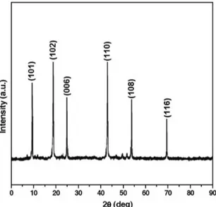
The phase composition and the structure of the ilm were studied by X‑ray diffraction analysis. The XRD patterns of CuSe thin ilms are shown in Figure 1. The excellent peaks (101), (102), (006), (110), (108), and (116) were obtained in the powder X‑ray diffraction studies. The peaks were compared with JCPDS diffraction patterns from the
[JCPDS Data File No.-00-020-1020]. The observed peaks corresponding to the formation of hexagonal phase of CuSe were indexed according to hexagonal structure. Knowing the wavelength (λ), full width at half maximum (FWHM) of the peaks (β), and the diffracting angle (θ), the particle size (D) was calculated by using the Scherrer formula,
. cos 0 9
D λ
β θ
= (1)
From the above relation, the average size of the CuSe was determined to be ≈ 37.5 nm which agreed ≈ well with the reported values of 38 nm[23].
3.2. SEM analysis
Scanning Electron Microscope (SEM) was used for studying the surface morphology and the micro structural features of the as‑prepared CuSe thin ilms. SEM image was obtained for CuSe thin ilm deposited on glass substrate in order to study the surface of the thin ilm. Figure 2 shows the SEM image of the CuSe thin ilms. The CuSe micrograph shows a compact structure composed of single type of small, densely packed microcrystals. The grains are well deined, spherical
Figure 1. XRD spectrum of CuSe thin ilms.
and of almost similar size. The increase in grain size leads to decrease in the grain boundaries, while in as-deposited ilm, the grains are of smaller size, more compact with a smooth grain background which is an indication of one-step growth by multiple nucleation.
3.3. AFM analysis
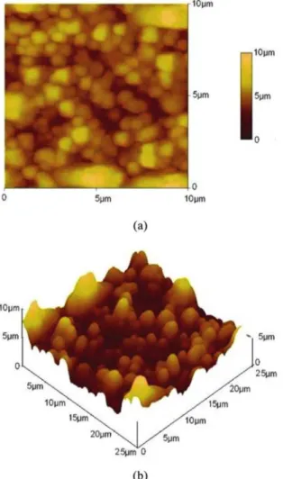
The surface morphology of the ilm was analyzed by Atomic Force Microscopy (AFM). Figure 3a, b show the AFM image of the as‑deposited CuSe thin ilms grown by CBD technique on the glass substrate. It is observed from the surface image that the particles are uniformly distributed on the surface of the ilm. From the 2D image, it is seen that the CuSe particles are found to agglomerate on the surface of the ilm. AFM images show the granular nature of the particles. This observation indicates that the ilm surface is somewhat rough.
3.4. Optical studies
Optical properties are very signiicant as far as applications in any optoelectronic devices are concerned. Optical band gap and absorption coeficient are the two important parameters of a solar cell material. In the present study,
optical characterization was done for the determination of the nature of absorption spectrum and the energy bandgap of CuSe thin ilms. The optical transmission spectrum of CuSe ilms was recorded in the wavelength region 400‑1400 nm and it is shown in Figure 4. It is important to note that CuSe ilms were very much transparent in the visible region. The dependence of optical absorption coeficient on photon energy helps to analyze the band structure and the type of transition of electrons.
The optical absorption coeficient (α) was calculated from transmittance using the following relation
log
1 1
d T
α =
(2)
where T is the transmittance and d is the thickness of the ilm. Determination of the optical band gap is based on the photon induced electronic transition between the conduction band and the valance band. As a direct band gap material, the ilm under study has an absorption coeficient (α) obeying the following relation for high photon energies (hν) and can be expressed as
/ ( g)1 2 A h E
hv ν
α= − (3)
where Eg is the band gap of the CuSe ilms and A is a constant. A plot of variation of (αhν)2 versus hν is shown in Figure 5. Using Tauc’s plot, the energy gap (Eg) was calculated to be 2.40 eV which agreed well with the reported values24. This was used to ind out the nature of transition in the thin ilm material.
3.4.1. Determination of optical constants
Two of the most important optical properties are the refractive index and the extinction coeficient which are generally called optical constants. The amount of light that transmits through thin ilm material depends on the amount of the relection and the absorption that take place along the light path. The optical constants such as the refractive index (n), the real dielectric constant (εr) and the imaginary part
Figure 3. AFM images of CuSe thin ilm (a) 2 dimension (2D) and
of the dielectric constant (εi) were calculated.The extinction coeficient (K) could be obtained from the following equation,
K 4 λα
π
= (4)
The extinction coeficient (K) was found to be 10.7 at λ =1400 nm.
The transmittance (T) is given by
(
)
(
)
(
)
exp
exp
2
2
1 R t
T
1 R 2 t
α α
− −
=
− − (5)
Relectance (R) in terms of absorption coeficient can be obtained from the above equation.
Hence,
exp( exp( ) exp( )
1 1 t t
R
1 t
± − −α + α
=
+ −α (6)
Refractive index (n) can be determined from the relectance data using the following equation,
( )
( )
2
R 1 3R 10R 3
n
2 R 1
+ ± + −
= −
− (7)
The refractive index (n) was found to be 2.3 at λ =1400 nm. The high refractive index makes CuSe ilm suitable for use in optoelectronic devices.
From the optical constants, electric susceptibility (χc) could be calculated using the following relation
2 2
r 0 4 C n k
ε =ε + πχ = − (8)
Hence,
2 2
0 C
n k
4 ε χ
π − −
= (9)
where ε0 is the permittivity of free space. The value of electric susceptibility (χc) was 4.29at λ=1400 nm. Since electrical susceptibility is greater than 1, the material can be easily polarized when the incident light is more intense.
The real part of the dielectric constant (εr) and the imaginary part of dielectric constant (εi) could be calculated from the following relations
2 2
r n k
ε = − (10)
i 2nk
ε = (11)
The values of the real dielectric constant (εr) and the imaginary dielectric constant (εi) at λ=1400 nm were estimated to be 3.756 and 9.802 x 10⁻⁵respectively.
The lower value of the dielectric constant and the positive value of the material were capable of producing induced polarization due to intense incident light radiation.
3.5. Dielectric studies
The dielectric constant was analyzed as a function of the frequency at different temperatures as shown in Figure 6, while the corresponding dielectric loss is shown in Figure 7. The dielectric constant could be evaluated using the relation,
r 0
Cd A ε
ε
= (12)
Figure 5. Plot of (αhν)[2] vs photon energy (hν).
Figure 6. Dielectric constant of CuSe thin ilms.
where ‘C’ is the capacitance, ‘d’ is the thickness of the ilms, ‘εO’ is the permittivity of free space, and ‘A’ is the
area of the ilms.
The plot between the dielectric constant and the frequency for various temperatures is shown in Figure 6. The curve reveals that the dielectric constant decreases with increase in frequency and then reaches almost a constant value in the high frequency region25. This also indicates that the value of the dielectric constant increases with an increase in the temperatures. The huge value of the dielectric constant at low frequencies can be attributed to the lower electrostatic binding strength, arising due to the space charge polarization near the grain boundary interfaces. Owing to the application of an electric ield, the space charges are stimulated and dipole moments are produced and are called space-charge polarization. This apart, these dipole moments are rotated by the ield applied ensuing in rotation polarization which also contributes to the high values. Whenever there is an increase in the temperature, more dipoles are produced and the value increases26. In the high frequency region, the charge carriers might have a tendency to move to higher values and dielectric constant falls to a low value before the ield reversal occurs. Figure 7 shows the variation of the dielectric loss with respect to the frequency for various temperatures. These curves show that the dielectric loss is dependent on the frequency of the applied ield, comparable to that of the dielectric constant. The dielectric loss decreases with an increase in the frequency at almost all temperatures, but appears to attain saturation in the higher frequency range at all the temperatures27,28.
In the proposed relation, only one parameter, viz., the high frequency dielectric constant is required as input, to evaluate electronic properties like valence electron plasma energy, average energy gap or Penn gap, Fermi energy and electronic polarizability of the CuSe thin ilms. The theoretical calculations show that the high frequency dielectric constant is explicitly dependent on the valence electron Plasma energy, an average energy gap referred to as the Penn gap and Fermi energy. The Penn gap is determined by itting the dielectric constant with the Plasmon energy29. The following relation30 is used to calculate the valence electron plasma energy, ћωP
/
.
1 2
p Z h 28 8
M
ρ ω =
(13)
According to the Penn model31, the average energy gap for the CuSe thin ilms is given by
(
)
/P
p 1 2
h E 1 ω ε∞ =
− (14)
where hωPis the valence electron plasmon energy and the
Fermi energy29 is given by
(
)
/. 4 3
F P
E =0 2948 hω (15)
Then, the electronic polarizability α is obtained using the relation32,33,
(
)
(
)
. 2 24 3 P 0 2 2P 0 P
h S M
0 396 10 cm
h S 3E
ω α ρ ω − = × × × + (16)
where S0 is a constant given by
2
P P
0
F F
E 1 E
S 1
4E 3 4E
= − +
(17)
The Clausius‑Mossotti relation,
a
1
3 M
4 N 2
ε α
π ρ ε∞∞ −
=
+
(18)
The following empirical relationship is also used to calculate α[34],
. .
g 24 3
E M
1 0 396 10 cm
4 06 α ρ − = − × × × (19)
Where Eg is the bandgap value determined through the UV transmission spectrum.
The high frequency dielectric constant of the materials is a very important parameter for calculating the physical or electronic properties of materials27. All the above parameters as estimated are shown in Table 1.
3.6. AC electrical conductivity studies
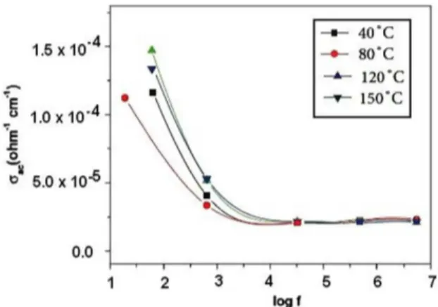
The conductivity of a material depends on its overall characteristics, such as its chemical composition, purity and crystal structure. Measurements taken with continuous currents provide only total conductivity. In the present study, electric ohmic contacts were made using air drying silver paint on the opposite faces. Electrical measurements were taken in the frequency range 20 Hz to 1 MHz using HIOKI 3532-50 LCRHITESTER. A chromel-Alumel thermocouple was employed to record the sample temperature. A 30 minute interval was used prior to thermal stabilization after each measuring temperature. All the measurements were carried out in atmospheric air.The temperature dependent AC electrical conductivity study was carried out. The temperature dependent AC conductivity of the CuSe thin ilms is shown in Figure 8. It is observed that the conductivity (σac) increases with an increase in the temperature and the frequency. The activation energy of the CuSe thin ilms was found to be 0.032 eV which agreed well with the reported values35. Figure 9 shows the temperature dependent conductivity of CuSe thin ilms. The igure indicates the exponential behavior of the temperature dependent current conirming the semiconducting property of the material36.
3.7. Photoconductivity studies
Photoconductivity is an important property of materials by means of which the conductivity of the material changes due to incident radiation. Photoconduction includes the
Table 1. Electronic parameters of the CuSe thin ilms.
Parameter Value
Plasma energy (hωp) 15.21 eV
Penn gap (Ep) 3.502 eV
Fermi Energy (EF) 11.009 eV
Electronic polarizability
(using the Penn analysis) 6.152 × 10 –24 cm3
Electronic polarizability
(using the Clausius‑Mossotti relation) 6.452 × 10 –24 cm3
generation and recombination of charge carriers and their transport to the electrodes. Obviously, the thermal and hot carrier relaxation process, charge carrier statistics, effects of electrodes, and several mechanisms of recombination are involved in photoconduction. Photoconductivity is due to the absorption of photons (either by an intrinsic process or by impurities with or without phonons), leading to the creation of free charge particles in the conduction band and/or in the valence band. It provides valuable information about physical properties of materials and offers applications in photodetection and radiation measurements. Field dependent dark and photoconductivity plots of CuSe thin ilms are shown in Figure 10. The plots indicate a linear increase of current in the dark and visible light illuminated CuSe thin ilms cases with an increase in the applied ield depicting the ohmic nature of the contacts37. It is observed from the igure that the photo current is always higher than the dark current and both the photo and the dark currents of CuSe thin ilms increase linearly with the applied voltage; thus photo current is more than the dark current which may be attributed to the generation of mobile charge carriers caused by the absorption of photon leading to positive photo conductivity. The low values of the dark current
and insigniicant rise in the photo current upon the visible light illumination are as expected. But the photocurrent is found to be more than the dark current. Hence it can be said that the material exhibits positive photo conductivity. This is caused by the generation of mobile charge carriers caused by the absorption of photons. This is because of an increase in the number of charge carriers or their life time in the presence of radiation. The positive photoconductivity of the ilms may be due to the increase in the number of charge carriers and it ascertains the conducting nature of the material. The dark current is less than the photocurrent, signifying positive photoconductivity nature conirmed by the reported results37,38.
3.8. I-V characteristics
I‑V characteristics of the CuSe thin ilms are shown in Figure 11. We can see that the lowing current through the ilm increases linearly with the increasing of the voltage of the electrodes. It is observed that the remarkably larger forward current at all voltages has been obtained and it implies the higher conductivity of these ilms. The remarkably increased conductivity may be helpful in obtaining higher eficiency in the solar cell.
Figure 11. I‑V characteristics of CuSe ilms. Figure 8. Variation of conductivity with log frequency.
Figure 9. Temperature dependent conductivity of CuSe thin ilms.
4. Conclusion
The CuSe thin films were prepared by chemical bath deposition (CBD) technique. The structural and the morphological properties of CuSe thin ilms were investigated by XRD and SEM methods. The XRD studies showed well the crystallized and cubic structure of CuSe thin ilms. The size and the morphology of the CuSe thin ilms were characterized by using SEM and AFM studies. The UV‑Visible transmission spectrum showed excellent transmission in the entire visible region. The optical properties such as band gap, refractive index, extinction coeficient, and electrical susceptibility were evaluated to analyze the optical property. The dielectric constant and
the dielectric loss of the CuSe thin ilms were calculated for different frequencies and temperatures. In addition, the plasma energy of the valence electron, Penn gap or average energy gap, the Fermi energy, and electronic polarizability of the CuSe thin ilms were also determined. AC electrical conductivity was found to increase with an increase in the temperature and the frequency. The activation energy was found to be 0.032 eV. The temperature dependent conductivity indicated the exponential behavior of the temperature dependent current conirming the semiconducting nature of the thin ilms. The photoconductivity study ascertained the positive photoconductivity nature of the CuSe thin ilms. I‑V characteristics of the CuSe thin ilms were also investigated.
References
1. Haram SK and Santhanam KSV. Electroless deposition of orthorhombic copper (I) selenide and its room temperature phase transformation to cubic structure. Thin Solid Films. 1994; 238(1):21-26. http://dx.doi.org/10.1016/0040-6090(94)90642-4. 2. Zhang Y, Qiao Z‑P and Chen XM. Microwave‑assisted elemental
direct reaction route to nanocrystalline copper chalcogenides CuSe and Cu2TeElectronic supplementary information (ESI) available: XPS spectra of the products. Journal of Materials
Chemistry. 2002; 12(9):2747-2748. http://dx.doi.org/10.1039/
b205558a.
3. Milman V. Klockmannite, CuSe: structure, properties and phase stability from ab initio modeling. Acta Crystallographica.
Section B, Structural science. 2002; 58(Pt 3 Pt 2):437-447.
PMID: 12037331.
4. Madelung LBO, Schulz M and Weiss H. Landolt‑börnstein. Berlin: Springer-Verlag; 2008.
5. Lakshmikumar S and Rastogi A. Selenization of Cu and In thin films for the preparation of selenide photo‑absorber layers in solar cells using Se vapour source. Solar Energy Materials and
Solar Cells. 1994; 32(1):7-19.
http://dx.doi.org/10.1016/0927-0248(94)90251-8.
6. Fadel M, Fayek SA, Abou‑Helal MO, Ibrahim MM and Shakra AM. Structural and optical properties of SeGe and SeGeX (X=In, Sb and Bi) amorphous films. Journal of Alloys and
Compounds. 2009; 485(1-2):604-609. http://dx.doi.org/10.1016/j.
jallcom.2009.06.057.
7. Gurin VS, Alexeenko AA, Zolotovskaya SA and Yumashev KV. Copper and copper selenide nanoparticles in the sol-gel matrices: structural and optical. Materials Science and Engineering C. 2006; 26(5-7):952-955. http://dx.doi.org/10.1016/j.msec.2005.09.021. 8. Heske C, Winkler U, Neureiter H, Sokolowski M, Fink R,
Umbach E, et al. Preparation and termination of well‑defined CdTe(100) and Cd(Zn)Te(100) surfaces. Applied Physics Letters. 1997; 70(8):1022. http://dx.doi.org/10.1063/1.118432. 9. Hermann AM and Fabick L. Research on polycrystalline thin‑
film photovoltaic devices. Journal of Crystal Growth. 1983; 61(3):664. http://dx.doi.org/10.1016/0022-0248(83)90195-1. 10. Oikkonen LE, Ganchenkova MG, Seitsonen P and Nieminen RM.
Redirecting focus in CuInSe 2 research towards selenium-related defects. Physical Review B: Condensed Matter and Materials
Physics. 2012; 86(16):165115. http://dx.doi.org/10.1103/
PhysRevB.86.165115.
11. Thanikaikarasan S, Mahalingam T, Kathalingam A, Moon H and Kim YD. Characterization of electrodeposited copper sulphide thin films. J. New Mater. Electrochem. Systems. 2010; 13:29-33.
12. Yakuphanoglu F and Viswanathan C. Electrical conductivity and single oscillator model properties of amorphous CuSe semiconductor thin film. Journal of Non-Crystalline Solids. 2007; 35(30-31):2934-2937. http://dx.doi.org/10.1016/j. jnoncrysol.2007.06.055.
13. Peranantham P, Jeyachandran YL, Viswanathan C, Praveena NN, Chitra PC, Mangalraj D et al. The effect of annealing on vacuum-evaporated copper selenide and indium telluride thin films. Materials Characterization. 2007; 58(8-9):756. http:// dx.doi.org/10.1016/j.matchar.2006.11.019.
14. Hankare PP, Khomane AS, Chate PA, Rathod KC and Garadkar KM. Preparation of copper selenide thin films by simple chemical route at low temperature and their characterization. Journal of
Alloys and Compounds. 2009; 469(1-2):478-482. http://dx.doi.
org/10.1016/j.jallcom.2008.02.062.
15. Lakshmikumar ST and Rastogi AC. Selenization of Cu and In thin films for the preparation of selenide photo-absorber layers in solar cells using Se vapour source. Solar Energy
Materials and Solar Cells. 1994; 32(1):7-19. http://dx.doi.
org/10.1016/0927-0248(94)90251-8.
16. Clement CL, Spaliart MN, Haram SK and Santhanam KVS. Chemical bath deposition of cubic copper (I) selenide and its room temperature transformation to the orthorhombic phase.
Thin Solid Films. 1997; 302:12. http://dx.doi.org/10.1016/
S0040-6090(97)00021-7.
17. Parkin IP. Solid state metathesis reaction for metal borides, silicides, pnictides and chalcogenides: ionic or elemental pathways. Chemical Society Reviews. 1996; 25(3):199. http:// dx.doi.org/10.1039/cs9962500199.
18. Garg JG, Sharma RP and Sharma KC. Characterization of p‑CuInSe2 films for photovoltaics grown by a chemical deposition technique. Thin Solid Films. 1988; 164:269-273. http://dx.doi.org/10.1016/0040-6090(88)90148-4.
19. Padam GK. The properties of chemically deposited Cu2−xSe thin films. Thin Solid Films. 1987; 150(1):L89-L92. 20. Chen WS, Stewart JM and Mickelson RA. Polycrystalline
thin-film Cu(2-x)Se/CdS solar cell. Applied Physics Letters. 1985; 46: 1095-1097.
21. Chu TL, Chu SS, Lin SC and Yue J. Large grain copper indium diselenide films. Journal of the Electrochemical Society. 1984; 131(9):2182. http://dx.doi.org/10.1149/1.2116044.
22. Tell B and Wiegand JJ. Photodetection properties of Cu2Se‑ AgInSe2 heterojunctions. Journal of Applied Physics. 1977; 48(12):5321. http://dx.doi.org/10.1063/1.323563.
Alloys and Compounds. 2009; 469(1-2):478-482. http://dx.doi. org/10.1016/j.jallcom.2008.02.062.
24. Bhuse VM, Hankare PP, Garadkar KM and Khomane AS. A simple, convenient, low temperature route to grow polycrystalline copper selenide thin films. Materials Chemistry and Physics. 2003; 80(1):82-88. http://dx.doi.org/10.1016/S0254-0584(02)00306-1. 25. Suresh S and Arunseshan C. Dielectric properties of cadmium
selenide (CdSe) nanoparticles synthesized by solvothermal method. Applied Nanoscience. 2014; 4(2):179-184.
26. Suresh S. Studies on the dielectric properties of CdS nanoparticles.
Applied Nanoscience. 2014; 4:325-329.
27. Sagadevan S. and Sundaram AS. Dielectric properties of lead sulphide thin films for solar cell applications. Chalcogenide
Letters. 2014; 11:159-165.
28. Sagadevan S and Murugasen P. Structural and electrical properties of copper sulphide thin films by chemical bath deposition method. International Journal of ChemTech Research. 2014; 6:5608-5611.
29. Bari RH, Ganesan V, Potadar S and Patil LA. Structural, optical and electrical properties of chemically deposited copper selenide films. Bulletin of Materials Science. 2009; 32(1):37-42. http:// dx.doi.org/10.1007/s12034‑009‑0006‑z.
30. Ravindra NM, Bharadwaj RP, Kumar KS and Srivastava VK. Model based studies of some optical and electronic properties of narrow and wide gap materials. Infrared Physics. 1981; 21(6):369-381. http://dx.doi.org/10.1016/0020-0891(81)90045-2. 31. Kumar V and Sastry BSR. Heat of formation of ternary
chalcopyrite semiconductors. Journal of Physics and Chemistry
of Solids. 2005; 66(1):99-102. http://dx.doi.org/10.1016/j.
jpcs.2004.08.034.
32. Penn DR. Wave‑number‑dependent dielectric function of semiconductors. Physical Review. 1962; 128(5):2093-2097. http://dx.doi.org/10.1103/PhysRev.128.2093.
33. Ravindra NM and Srivastava VK. Properties of liquid PbS, PbSe and PbTe. Infrared Physics. 1980; 20(6):399-418. http:// dx.doi.org/10.1016/0020-0891(80)90058-5.
34. Reddy RR, Ahammed YN and Kumar MR. Variation of magnetic susceptibility with electronic polarizability in compound semiconductors and alkali halides. Journal of Physics and
Chemistry of Solids. 1995; 56(6):825-829. http://dx.doi.
org/10.1016/0022-3697(94)00268-1.
35. Dhanam M, Manoj PK and Prabhu RR. High‑temperature conductivity in chemical bath deposited copper selenide thin films. Journal of Crystal Growth. 2005; 280(3-4):425. http:// dx.doi.org/10.1016/j.jcrysgro.2005.01.111.
36. Thirumavalavan S, Mani K and Suresh S. Investigation on structural, optical, morphological and electrical properties of lead sulphide (PbS) thin films. Journal of Ovonic Research. 2015; 11:123-130.
37. Thirumavalavan S, Mani K. and Sagadevan S. Structural, surface morphology, optical and electrical investigation of cdse thin films. Chalcogenide Letters. 2015; 12:237-246.
![Figure 5. Plot of (αhν) [2] vs photon energy (hν).](https://thumb-eu.123doks.com/thumbv2/123dok_br/18881769.422828/4.765.399.710.431.748/figure-plot-αhν-vs-photon-energy-hν.webp)