*e-mail: [email protected]
1. Introduction
Magnetostrictive thin ilms with lower saturation ield and coercivity; and higher magnetostriction coeficient have applications in magnetic micromechanical systems1. Since its inception into the world of advanced functional material research, FeGa alloys have gained much popularity and piqued the interest amongst the scientiic community owing to their superior mechanical and magnetostrictive properties on comparison with its already in market counterparts like Terfenol-D and shape memory alloys. There are ive phases that can co-exist in the FeGa alloys and thin ilms, namely, a disordered bcc α – Fe phase (A2), an ordered bcc superlattice phase (DO3), an ordered fcc phase (L12), an ordered hexagonal close packed phase (DO19) and an ordered bcc phase (B2) as per the currently available literature. The presence of DO3 structure is said to be detrimental for obtaining high magnetostrictive property of FeGa alloys or ilms2,3. It is proposed that one could extract maximum magnetostriction from these materials when it has A2 phase4. For magnetostrictive devices, magnetoelastic material in the form of thin ilms with high magnetostriction constant and low saturation ield are desired. There are many results on single crystalline and polycrystalline bulk Galfenol with varying compositions. Gaudet et. al.3, have prepared Fe
100-xGax alloys by mechanical milling and reports low degree of Ga clustering in as milled powders which is indicative to the
commencement of short range DO3 ordering and shows the formation of DO3 and L12 order in annealed samples. Basumatary et. al.5 have also reported the presence of all the three phases (A2, DO3, L12 ) in FeGa alloy. Zhang et. al.
6,
found the DO3 structure and Ga-rich cluster formation in melt spun ribbons which enhanced their giant magnetostriction. Limited literature is available on RF sputtered galfenol thin ilms1. Morley et. al.7, prepared FeGa thin ilms of varying compositions using a customised deposition procedure using both co-sputtering and evaporation process. This was done to facilitate lexibility in the ilm composition by varying the evaporation rate and sputtering power of the target. Javed et. al.8, successfully deposited single phase b.c.c. FeGa thin ilms which had weak uniaxial anisotropy at lower Ar pressure and exhibited isotropic nature on increased Ar pressure. However, there was no change in magnetostriction constant with respect to varying pressure. Butera et. al.9,10, have successfully grown FeGa ilms with cubic magnetic symmetry on MgO substrates. Basantkumar et. al.1, fabricated FeGa ilms on thin glass cover slides using RF sputtering and studied how the forward power affects its composition and magnetic properties. These groups also succeeded in integrating these ilms with MEMS cantilevers for magnetic actuation. Present study attempts to fabricate Galfenol thin ilms by RF sputtering on different substrates varying the deposition parameters and understanding their structural and magnetic properties.
Growth and Magnetic Properties of RF Sputtered Fe-Ga Thin Films
Lalitha Raveendran Niveditaa, Valiveti Venkata Siva Kumarb, Kandasami Asokanb,
Ramasamy Thangavelu Rajendrakumara,c*
aAdvanced Materials and Devices Laboratory, Department of Physics, Bharathiar University, Coimbatore, India Pin - 641046
bMaterials Science Division, Inter University Accelerator Centre, New Delhi, India Pin -110 067 cDepartment of Nanoscience and Technology, Bharathiar University, Coimbatore, India Pin – 641046
Received: November 11, 2014; Revised: February 7, 2015
We report the growth and characterization of Fe-Ga thin ilms. These ilms were RF sputtered onto Si, MgO and quartz substrates by controlling the parameters such as the deposition time, power and substrate temperature. The deposited ilms were characterized using X-Ray Diffraction, Atomic Force Microscopy and Vibration Sample Magnetometry measurements. The effect of substrates on the structure and magnetic properties were studied. XRD pattern of the deposited ilms showed the formation of DO3 phase with L12 ordered structure at higher sputtering power. The room temperature deposited ilms demonstrated higher magnetization (0.08 emu/g) as compared to higher substrate temperature (300 oC) deposited ilms. The Mr/Ms ratio was found to be 0.037 for ilms deposited at room temperature and 0.009 for the substrate temperature 300 oC. L1
2 order was observed in ilms deposited on MgO and Quartz substrates. Magnetization was also found to be high (Ms out of plane = 518 emu/cm3, M
s in plane = 707 emu/cm
3) for ilms deposited on MgO substrate.
Keywords: Fe-Ga thin ilms, RF sputtering, annealing, in plane magnetization, out plane
Growth and Magnetic Properties of RF Sputtered Fe-Ga Thin Films
2015; 18(5) 947
2. Experimental Methodology
Thin Films of FeGa were prepared by RF Magnetron sputtering under different deposition conditions. The RF sputtering unit was a custom made instrument in the Inter University Accelerator Centre (IUAC), New Delhi. The ilms were prepared at different conditions by varying sputtering parameters such as sputtering power and substrate temperature. FeGa alloy 2” diameter target was RF sputtered with power PSp, which was varied as 80, 100, 120 and 140 W. The typical base chamber pressure was 6.5×10⁻⁵ torr and the argon working pressure was kept constant for all depositions at 6.5×10⁻² torr. The ilms were deposited onto Si substrates at room temperature and at 300 °C by varying the time of deposition and substrate temperature along with sputter power. By varying the time of deposition as 45 min, 90 min and 180 min, we obtained ilms of thickness ~20nm, ~40nm, ~100nm. 20nm ilms were deposited at all the four PSp at both room temperature and 300 °C, 40 nm ilms at PSp of 100W at room and 300 °C substrate temperature and 100nm ilms at PSp 80W and 140W at room and 300 °C substrate temperature. The structural analysis of the ilms was done by taking their 2θ X-Ray scans using glancing incidence X-ray diffractometer (GIXRD), Bruker, D-8 model and Surface morphology analysis was done by Atomic Force Microscopy (AFM), Veeco Instruments Inc.. Magnetic properties of these ilms were measured by Vibration Sample Magnetometer (VSM), EV-9, Microsense.
3. Results and Discussion
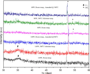
The XRD pattern of the alloy target had two main peaks with (110) relection at 43.6o and (200) relection at 63.4o that corresponds to A2 structure. Though this is the most likely crystal structure, it could also be that of DO3 (Fe3Al type, α”), which have X-ray diffraction relections at (220) for 43.6o peak and (400) for 63.4o[2,11], since the alloy composition is in the range of 25 between 25 and 30%. The same peaks were expected in the sputtered ilms also. But the XRD showed a predominant peak at ~52o in all the ilms deposited at different sputtering powers. There were some other relections present along with this predominant peak under selected sputtering conditions.
The XRD 2θ scans of 20 nm, 40 nm and 100 nm thick ilms fabricated by varying PSp were taken. For 20 nm and 40 nm thick ilms, two peaks were observed at ~52o and ~55o corresponding to the (311) and (222) relections originating from DO3 ordering. The high intensity relection at ~52o clearly identiies the presence of DO3 ordering2,6. The (222) relection is of much less intensity. From all the ilms deposited on Si at various PSp’s, we have concentrated on 100 nm thick ilms under extreme PSp conditions, namely, 80W and 140W. The ilms deposited at other conditions were not uniform. Figure 1 shows the XRD patterns of 100nm thick ilms fabricated at two PSp, 80W and 140W. We observed the presence of DO3 structure in all the ilms. Room temperature prepared ilms deposited at both the PSp demonstrates the presence of the (311) relection while (222) relection is absent in higher PSp deposited ilm. There is evolution of a peak at ~35o in these ilms, which corresponds to that of (110) relection of L12. Sputtering at higher PSp could have resulted in mixed phase
formation of FeGa, with both L12 and DO3 structure presence in the ilm. The above mentioned room temperature deposited ilms were annealed in vacuum for three hours at 500 °C. The (110) relection was found to completely vanish after annealing. This indicates the probable rearrangement of lattice system of FeGa where L12 phase gets rearranged to form DO3. The crystallite size calculated using Debye-Scherrer formula was in the range of 75 – 90 nm for all the ilms. There was substantial increase in the crystallite size (~135 nm) after the ilms were annealed. We have optimised the ambient deposition condition for the ilms on Silicon to be 140W with 300 °C substrate temperature for a deposition time of 180 min, because it delivers uniform and homogenous ilms.
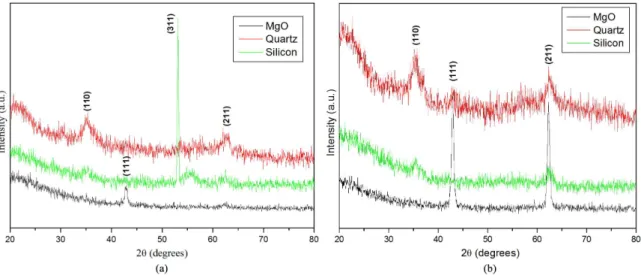
There are various reports of FeGa ilms deposited onto metallic underlayers9,12-14 and substrates other than Si and glass. After optimisation, a set of ilms were deposited on MgO and Quartz substrates along with Si, at PSp 140W, 300 °C substrate temperature for 180 min to see how substrate affects the ilms. The ilms were approximately 100 nm thick. The as-prepared ilms were also annealed in vacuum at 500 °C for three hours. The XRD scans of the as-prepared and annealed ilms are given in Figure 2a and b.
The ilm deposited on Si substrate had (311) relection of DO3 which was the predominant peak. The other relections at ~35o and ~62o with (110) and (211) orientations identify the presence of partial L12 ordering in the ilm. There is also the presence of a relection at ~55o which could be either (222) orientation of DO3[2] or (210) orientation of L1
2 ordering 2. The ilms on Quartz substrate exhibits only (110) and (211) relections of L12. The dominant relection on MgO substrate is at ~43o which belongs to (111) relection of L12. The only other peak corresponds to (211) orientation of L12.
The X-ray data of ilms on different substrates (Figure 2) conirms the partial long range ordering of DO3 and L12 structures on different substrates. While Si is the only substrate that favours the development of DO3 long range order (though with the presence of L12 order), MgO and Quartz substrate favours the ilm deposition in L12 ordered structure. The L12 (110) and (211) relections in annealed ilm on Quartz substrate slightly improves in intensity with
Figure 1. X-Ray diffraction patterns of 100 nm thick FeGa thin ilms
a shift of 0.2o to higher 2θ value while they show a shift of ~0.1o to the lower 2θ value in Si substrate with the complete disappearance of the previously dominant DO3 relection. The disappearance of DO3 relection can only mean that lattice rearrangement occurred. But this is at total contradiction with the result from what we observed in the room temperature deposited ilms. There, the lattice rearrangements lead to complete formation of DO3 whereas, here the inverse effect is observed. The shift in the peak 2θ value can also be attributed to the lattice rearrangements. The L12 relections of FeGa on MgO increases in intensity on annealing which manifests betterment of crystallinity of the ilm.
The calculation of microstrain on ilms (Table 1) due to the substrate was carried out and it was found that the ilms on MgO substrates indicated low strain thus manifesting the fact that it may be a better suited substrate for the nucleation and growth of thin ilms. The microstrain on quartz and Silicon substrates were 3 times greater when compared with MgO. The microstrain was calculated for the dominant peak present in the ilms in each substrate. The earlier reports mentioning that the lattice mismatch is minimal for FeGa/MgO is afirmed by the minimal strain in thin ilms.
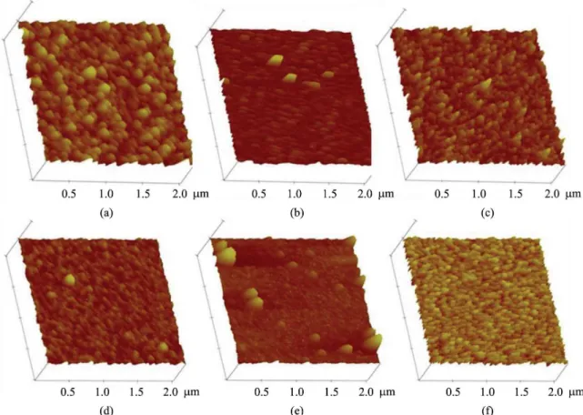
The surface morphology of the deposited thin ilms was observed using Atomic Force Microscopy. Figure 3 shows the AFM images of the as-deposited and annealed 100 nm thick FeGa thin ilms. The ilms deposited were uniform and the line scans across the AFM images gave the average grain diameter to be in the range of 75-120 nm in as deposited ilms while it was 45-55 nm in annealed thin ilms.
It was seen from XRD that the grain size increased on annealing the as deposited ilm. But this was contrary to what we observed in AFM data. The grain size here reduced drastically from ~110 to ~55nm. It can be inferred that there is columnar grain growth during annealing. The variation in grain size could be due to the presence of inhomogeneous strains in the ilm8. The RMS values of the surface roughness of the ilms were below 2 nm.
The M-H hysteresis loops for the 100nm thick ilms (140W) fabricated on Si substrates are shown in Figure 4.
Both room temperature and 300 °C substrate temperature deposited ilms demonstrate soft magnetic property.
The room temperature deposited ilms showed higher saturation magnetisation (0.08 emu/g) than the higher substrate temperature deposited ilms (0.06 emu/g). The coercivity of ilms deposited at room temperature is 87.697 G with Mr/Ms ratio of 0.03724 while for higher substrate temperature deposited ilm, coercivity is 12.809 G and the Mr/Ms ratio is 0.00918.
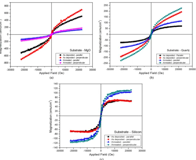
The hysteresis loops for the ilms deposited on different substrates are plotted in Figure 5. The effect of substrate on M of the ilms manifests in as deposited ilms. The magnetization is highest for ilms on MgO with Ms// =512 emu/cm
3 and
Ms┴= 699 emu/cm3 (Refer Table 2). Magnetization of ilms deposited on Si and Quartz substrates are in the similar range. On annealing, the overall magnetization reduces with its value being comparable in all substrates, though a slight higher Ms┴ value is observed for quartz. The Ms┴ / Ms// ratio was found to be more or less the same for MgO and Si substrate whereas this is much higher for quartz.
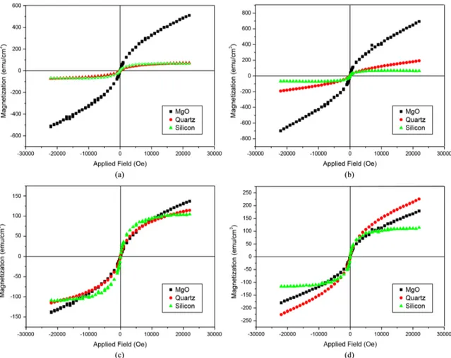
The hysteresis loops for ilms deposited on different substrates for both as deposited and annealed conditions were plotted as in Figure 6. It is observed that the magnetisation value is higher for as-deposited ilm on MgO. On annealing, the magnetization of ilm decreases in both in plane and out of plane directions. The magnetization values improve after annealing for ilms on Quartz and Silicon. For fcc L12 order, the easy axis of magnetization is (111) which is present in the ilms deposited on MgO substrate. The higher value Figure 2. X-Ray diffraction patterns of FeGa thin ilms on different substrates a) as-deposited b) annealed at 500 °C.
Table 1. The microstrain values calculated from Fe-Ga thin ilms
on different substrates.
Substrate
Microstrain (x10-3)
As prepared Annealed As prepared / annealed
MgO 2.7248 1.7278 1.5770
Silicon 8.3445 2.0556 4.0594
Growth and Magnetic Properties of RF Sputtered Fe-Ga Thin Films
2015; 18(5) 949
Figure 3. a) AFM images of FeGa thin ilms deposited at 140W at a) Room temperature b) 300 °C substrate temperature c) 140W Annealed
@ 500 °C for three hours d) 80W deposited at Room temperature e) 300 °C substrate temperature f) 80W Annealed @ 500 °C for three hours.
Figure 4. Magnetic ield dependence of Magnetisation of as-deposited (140W) FeGa thin ilms on Si substrate. In the inset, we have the
of magnetization for as deposited ilms on MgO may be attributed to the presence of (111) plane which favours easy axis of magnetization. The DO3 has (311) plane present which corresponds to the hard axis of magnetization for a bcc crystal as can be seen from the hysteresis loop. The miller planes in as prepared ilm on MgO exhibited increase in intensity on annealing, with both (111) and (211) planes equally increasing in intensity. The decrease in magnetization after annealing, in MgO substrate, could be due to the miller planes
being present in opposite direction which may annihilate the magnetization achieved by both miller planes. Quasilinear loops are obtained when magnetization was measured parallel and perpendicular to the deposited ilm.
There is enhanced magnetisation and retention of L12 order in the ilm which could be attributed as an inluence of MgO on the ilm. The microstrain calculation also indicated the favourability of MgO as a suitable substrate for Fe-Ga ilm growth. It has been mentioned elsewhere10 that relative Figure 5. Magnetic ield dependence of Magnetisation of as-deposited (140 W, 300 °C substrate temp.) FeGa thin ilms measured a) parallel
to the ilm b) perpendicular to the ilm c) annealed (500 °C) FeGa thin ilms measured parallel to the ilm d) perpendicular to the ilm.
Table 2. The saturation magnetisation values of 140W, 300 °C substrate temp. deposited thin ilms as obtained from the VSM measurement.
Substrate Measurement parameters As prepared Annealed
MgO Ms// (emu/cm
3) 518 139
Ms┴ (emu/cm
3) 707 182
Ms┴/Ms// 1.365 1.309
Quartz Ms// (emu/cm
3) 79.56 117
Ms┴ (emu/cm3) 204 229
Ms┴/Ms// 2.55 1.957
Si Ms// (emu/cm3) 64.96 107
Ms┴ (emu/cm3) 86 119
Growth and Magnetic Properties of RF Sputtered Fe-Ga Thin Films
2015; 18(5) 951
small lattice mismatch between MgO and FeGa (cubic with ~0.7% lattice mismatch) favours good nucleation and growth of thin ilms.
4. Conclusions
The structure and magnetic properties of FeGa thin ilms grown by RF magnetron sputtering technique have been investigated. It was found that long-range ordered DO3 structure was formed in all sputter conditions, but for high sputter power of 140W in 100 nm thick ilms, coexistence of L12 and DO3 phases were observed. On annealing this ilm, lattice rearrangement occurred leading to the disappearance of L12 phase, leaving only DO3 in the ilm. The effect of substrates on the structure and magnetic properties were
also studied and it was observed that the MgO substrate favoured higher magnetization when compared to Si and Quartz substrates. An anomalous behaviour was observed when 100 nm thick 300 °C deposited ilm on Si substrate was annealed. The ilms on MgO and Quartz retained L12 order and there was enhanced magnetization for ilms on MgO substrate.
Acknowledgements
The authors RTR and NLR would like to thank University Grants Commission - Inter University Accelerator Centre, New Delhi for the inancial support provided through the UGC – IUAC project (IUAC/XIII.7/UFR-51311/2677). Figure 6. In plane and Out-of-plane M-H curves of as-deposited and annealed Fe-Ga thin ilms on different substrates a) MgO b) Quartz
c) Silicon.
References
1. Basantkumar RR, Stadler BJH, Robbins WP and Summers EM. Intergration of thin-film galfenol with MEMS cantilevers for
magnetic actuation. IEEE Transactions on Magnetics. 2006;
42(10):3102-3104. http://dx.doi.org/10.1109/TMAG.2006.879666. 2. Lograsso TA, Ross AR, Schlagel DL, Clark AE and Wun-Fogle
M. Structural transformations in quenched Fe-Ga alloys. Journal
of Alloys and Compounds. 2003; 350(1-2):95-101. http://dx.doi.
org/10.1016/S0925-8388(02)00933-7.
3. Gaudet JM, Hatchard TD, Farrell SP and Dunlap RA. Properties of Fe-Ga based powders prepared by mechanical alloying. Journal of Magnetism and Magnetic Materials. 2008; 320(6):821-829.
http://dx.doi.org/10.1016/j.jmmm.2007.08.029.
4. Javed A, Szumiata T, Morley NA and Gibbs MRJ. An investigation
behaviour of Fe-Ga alloy thin films. Acta Materialia. 2010; 58(11):4003-4011. http://dx.doi.org/10.1016/j.actamat.2010.03.023.
5. Basumatary H, Palit M, Arout Chelvane J, Pandian S, Manivel Raja M and Chandrasekaran V. Structural ordering and magnetic
properties of Fe100-xGax alloys. Scripta Materialia. 2008; 59(8):878-881. http://dx.doi.org/10.1016/j.scriptamat.2008.06.034.
6. Zhang MC, Gao XX, Jiang HL, Qiao Y and Zhou SZ. Effect
of Ga content on the magnetostriction and microstructure of Fe-Ga ribbons’. Journal of Alloys and Compounds. 2007; 431(1-2):42-44. http://dx.doi.org/10.1016/j.
jallcom.2006.05.093.
7. Morley NA, Yeh SL, Rigby S, Javed A and Gibbs RJ. Development
of a cosputter-evaporation chamber for Fe-Ga films. Journal of
Vacuum Science & Technology. A, Vacuum, Surfaces, and Films. 2008; 26(4):581-586. http://dx.doi.org/10.1116/1.2924416.
8. Javed A, Morley NA and Gibbs MRJ. Structure, magnetic
and magnetostrictive properties of as-deposited Fe-Ga thin films. Journal of Magnetism and Magnetic Materials. 2009; 321(18):2877-2882. http://dx.doi.org/10.1016/j.jmmm.2009.04.039.
9. Butera A, Gomez J, Barnard JA and Weston JL. ‘Magnetic
anisotropy in Fe81Ga19/MgO (100) films sputtered at different
powers. Physica B, Condensed Matter. 2006; 384(1-2):262-264.
http://dx.doi.org/10.1016/j.physb.2006.06.005.
10. Butera A, Gomez J, Weston JL and Barnard JA. Growth and magnetic characterization of epitaxial Fe81Ga19/MgO (100) thin
films. Journal of Applied Physics. 2005; 98(3):033901. http:// dx.doi.org/10.1063/1.1996829.
11. Kawamiya N, Adachi K and Nakamura Y. Magnetic properties
and mossabauer investigations of Fe-Ga alloys. Journal of the
Physical Society of Japan. 1972; 33(5):1318-1327. http://dx.doi. org/10.1143/JPSJ.33.1318.
12. Adolphi B, McCord J, Bertram M, Oertel C-G, Merkel U,
Marschner U, et al. Improvement of sputtered Galfenol thin films for sensor applications. Smart Materials and Structures. 2010; 19(5):055013. http://dx.doi.org/10.1088/0964-1726/19/5/055013.
13. Butera A, Weston JL and Barnard JA. Ferromagnetic resonance
of epitaxial Fe81Ga19 (110) thin films. Journal of Magnetism and Magnetic Materials. 2004; 284:17-25. http://dx.doi.
org/10.1016/j.jmmm.2004.06.015.
14. Weston JL, Butera A, Lograsso T, Shamsuzzoha M, Zana I, Zangari G, et al. Fabrication and characterization of Fe81Ga19