Bidirectional Boost/Buck Quadratic Converter
for Distributed Generation Systems with
Electrochemical Storage Systems
D. Foito
ESTSetubal, Polytechnic Institute of Setúbal Setúbal, Portugal
daniel.foito@estsetubal.ips.pt
A. Cordeiro
ISEL – Polytechnic Institute of Lisboa Lisboa, Portugal
acordeiro@deea.isel.ipl.pt
Abstract—The increasing number of distributed generation systems using renewable and non-conventional energy sources show the trend of future generation systems. Most of these systems require power electronic converters as an interface between the DC voltage buses and electrochemical storage systems. Such storage systems, like batteries or supercapacitors, usually need bidirectional DC-DC converters to allow their charge or discharge according with necessary operation conditions. In this paper, a non-isolated bidirectional Buck-Boost converter with high voltage gain for electrochemical storage devices used in distributed generation systems is presented. To achieve high voltage gain ratios, the proposed topology presents quadratic characteristics in both step-down (Buck) and step-up (Boost) operation modes. In addition to the wide conversion range, it presents continuous input and output current, reduced charging/discharging ripple and simple control circuitry. All these features allow the energy exchange smoothly and continuously resulting in a longer durability of storage devices. The principle of the operation of the proposed converter in both operation modes, as well as their theoretical analysis will be discussed. The performance of this bidirectional power converter is confirmed through simulation and experimental results.
Keywords— bidirectional DC/DC converter, Boost and Buck quadratic converter, distributed generation systems.
I. INTRODUCTION
The investment in renewable and sustainable energy sources is continuously increasing. According with data available from
2015 the global new investment in renewable energy and fuels climbed to a record USD 285.9 billion [1]. Furthermore, a
significant interest over the last years about losses over long transmission and distribution lines, reduction of installation costs and
voltage regulation problems have encouraged the development of distributed generation systems based on photovoltaic panels
(PV), fuel cells (FC), wind turbine, micro-turbines, etc., allowing small-scale generation located near to the customers rather than
remote locations [2, 3]. Also remarkable is the increasing number of other applications (telecommunications systems, hybrid
electric vehicles, aviation, uninterruptible power supplies, etc.) using non-conventional energy sources [4-8]. Undesirably the
floating nature of most renewable energy sources makes them unsuitable for standalone operation as the sole power source. For
instance, hydrogen and hydrocarbon fuel cells contain high electrochemical energy but usually require back-up power at starting
conditions [9, 10]. The most common solution to overcome this problem is to use energy storage devices such as batteries or
super-capacitor in addition to the renewable energy source to compensate for these fluctuations and maintain a smooth and continuous
between storage devices and the rest of the system. Besides the adaptation to different voltage levels these converters will also
control the charge or discharge of storage devices according with required operating condition. Several bidirectional DC-DC
converters based on isolated and non-isolated topologies have been presented in literature for this purpose [12-17]. Most of isolated
topologies need a transformer and a high number of switching devices which increases the cost and the switching losses, in addition
to more complicated control schemes [18-21]. Non-isolated topologies are mainly based on the conventional Buck-Boost and Cuk
configurations which are fairly simple and easy to control [22-25]. However, in many applications the high gain requirements are
such that the conventional DC-DC converter operates with extremely duty-cycle operation which may result in reverse-recovery
problem and causes not only low efficiency but also creates electromagnetic interference (EMI) problems [13]. To extend the
voltage gain ratio, several DC-DC converters with magnetic coupling techniques have been proposed, notwithstanding some
disadvantages such as pulsating bus voltage remain and complex control schemes [26, 27].
In this paper, a non-isolated bidirectional Buck-Boost quadratic converter is proposed. This solution is suitable for distributed
generation systems where conventional converters are inadequate for high-frequency applications and where the specified range of
input voltages and the specified range of output voltages call for an extremely large range of conversion ratios. This converter with
quadratic DC conversion ratio offer a significantly wider conversion range, continuous input and output current, reduced
charging/discharging ripple and also simple control circuitry.
II. BIDIRECTIONAL BOOST/BUCK QUADRATIC CONVERTER
One of the most known topologies with wide voltage range is the Boost quadratic converter. As can be seen by Fig. 1, this
topology is characterized by the use of two inductors, one intermediate capacitor, three diodes and a single power switch.
Fig. 1. Classical quadratic Boost converter.
In order to overcome the limitation of the unidirectional power flow of the Boost quadratic converter it is proposed a new
bidirectional power converter. Fig. 2 shows the power topology of this converter. As presented in this figure, the power circuit does
not require more passive components (inductors and capacitor) than the required by the classical Boost quadratic converter. It is
also characterized by a static voltage gain with a quadratic function for both Boost and Buck operating modes.
In order to analyze the proposed bidirectional dc/dc converter will be assumed steady state operation, continuous conduction
mode (CCM) and ideal components. As described, the proposed power converter allows for two distinct modes of operation:
discharging and charging of the storage system.
III. OPERATION OF THE POWER CONVERTER
In the discharging mode the converter operates as a Boost converter, transferring the energy from the storage system to the load.
In this mode two of the transistors (T1 and T4) are always in the OFF state and the transistor T3 is always in the ON state. This mode
is also characterized by two equivalent circuits during one switching cycle (Ts), as described below:
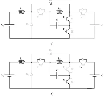
First equivalent circuit (Fig. 3 a)): This circuit is obtained when the transistor T2 is in the ON state (during the time interval of
δTs). In this state the inductors L1 and L2 will be charged since the currents in these inductors will increase linearly. The energy
stored in the capacitor C is transferred to the inductor L2.
Second equivalent circuit (Fig. 3 b)): This circuit is related with the transistor T2 in OFF state (during the time interval of
(1-δTs). This state is characterized by the discharge of the inductors L1 and L2. During this time interval the currents in these inductors
will decrease linearly. The energy that was stored in the previous state is now transferred to the capacitor C and to the load:
a)
b)
Fig. 3. Equivalent circuits during one switching period for the discharge mode of the storage system.
From the analysis of these two operating stages is possible to obtain the voltage gain of this converter in discharge mode and in
CCM. Thus, considering that the average voltages in the inductors in the two operating stages are equal, the following relationships
are obtained
0
1− − =
+( )(V V )
Vi δ i C
δ (1)
0
1− − =
+( )(V V )
VC δ C o
δ (2)
From the partial voltage gains that are obtained from the previous equations, the input to output voltage gain in this discharge
2 1 1 ) ( V V i o δ − = (3)
The operation of the converter in charging mode is characterized by the energy transfer from the load to the storage energy
system. In this mode of operation the converter operates as a Buck converter. As in the previous operation mode in this case only a
single transistor controls the output voltage through commutation. Thus, the transistors T2 and T3 are always in the OFF state. The
transistor T4 could be always in the ON state or can commutate at the same time with transistor T1 (additional switching losses).
From the analysis of this operating in CCM is possible to verify that during one switching cycle there are two equivalent circuits, as
following described:
First equivalent circuit (Fig. 4 a)): This first equivalent circuit is related with the on-time (time interval of δTs) of transistor T1.
During this time period the currents in inductors L1 and L2 will increase in absolute value. Capacitor C will discharge since its
energy will be transferred to inductor L1.
Second equivalent circuit (Fig. 4 b)): The obtained circuit associated to the complementary time (time interval of (1-δTs) is
related with the transistor T1 in OFF state. In this state the currents in the inductors L1 and L2 will decrease in absolute value. The
energy that was stored in those inductors will be transferred to the capacitor C and to the load (storage system).
a)
b)
Fig. 4. Equivalent circuits during one switching period for the charge mode of the storage system
The relationship between the output and input voltage of the converter in discharge mode in CCM can be obtained from the
analysis of the equivalent circuits presented in Fig. 4. Thus, according to these circuits and considering that the sums of the average
voltages in the inductors during one switching cycle are equal to zero, the next relationships are obtained:
0
1− =
−
− i i
C V ) ( )V
V
( δ
δ (4)
0
1− =
+ −
C o
C V ) ( )V
V
( δ
The input voltage gain of this converter in discharge mode will therefore be given by the partial voltage gains that can be
obtained from the previous equations, as follows:
2
δ =
i o
V V
(6)
IV. SIMULATION RESULTS
The operation modes of the proposed bidirectional Boost/Buck quadratic converter were verified through numerical
simulations. These simulations were performed using the Matlab/Simulink program. The converter operation was verified at Vi =
24V (battery voltage), Vo = 200V, L1 = 1 mH, L2 = 2 mH C = 150 µF and switching frequency fs = 14 kHz.
In the discharge mode it is considered the voltage of the storage as the input and the Vo as the output voltage. Figures 5, 6 and 7
show the obtained simulated results for the converter, operating in discharging mode (quadratic Boost) and CCM. These results
were obtained for a duty cycle of 0,66. In Fig. 5 is possible to verify the input voltage (1), capacitor voltage (2) and output voltage
(3). The high gain of the power converter is confirmed by this result. Figs. 6 and 7 show the inductor currents iL1 and iL2 and the
voltage at the terminals of transistors T1 and T2. From these figures is possible to confirm the continuous inductor current operation.
The ripple current in both inductors are also similar in magnitude.
Fig. 5. Discharging mode. Simulation waveforms of the: 1 – input voltage Vi, 2 - capacitor voltage Vc and 3 - output voltage Vo.
Fig. 7. Discharging mode. Simulation waveforms of the transistor T2 voltage (VT2) and inductor L2 current (iL2).
The operation in charged mode (quadratic Buck) was also confirmed through the simulations. Figs 8-10 show the obtained
simulated results in this mode of operation for a duty cycle of 0,35. The input voltage (1), capacitor voltage (2) and output voltage
(3) are presented in Fig. 8. As expected, in this case the output voltage (storage system) is much lower than the input voltage. The
inductor currents iL1 and iL2 and the voltage at the terminals of transistors T1 (VT1) and T2 (VT2) are presented in Figs. 9 and 10.
From these figures is possible to confirm the continuous inductor current. Even in this mode the ripple current in both inductors are
still similar in magnitude.
Fig. 8. Charging mode. Simulation waveforms of the: 1 – input voltage Vo, 2 - capacitor voltage Vc and 3 - output voltage Vi.
Fig. 10.Charging mode. Simulation waveforms of the transistor T2 voltage (VT2) and inductor L2 current (iL2).
V. EXPERIMENTAL RESULTS
A prototype of the proposed converter was built to validate the theoretical considerations and obtained simulation results. The
circuit parameters of the experimental prototype are the same as those used for simulation. As made for the simulation the
prototype was verified in the discharging mode (Vi =24V → Vo=200V) and charging mode (Vo =200V → Vi=24V) power flow.
The waveforms obtained from the experimental prototype in discharging power flow mode (quadratic Boost) are presented in
Figs. 11, 12 and 13. All these results were obtained for a duty cycle of 0,67. From Fig. 11 is possible to confirm that the input
voltage (1), capacitor voltage (2) and output voltage (3) are in agreement with the expected. This figure also confirms the high gain
of the power converter. Figs. 12 and 13 show the inductor currents iL1 and iL2 and the voltage at the terminals of transistors T1 (VT1)
and T2 (VT2). Through these figures is possible to confirm the expected continuous inductor current operation. They also show that
the ripple current in both inductors are also similar in magnitude.
Fig. 11.Discharging mode. Experimental waveforms of the: Ch1 – input voltage Vi, Ch2 - capacitor voltage Vc and Ch3 - output voltage Vo.
Fig. 13.Discharging mode. Experimental waveforms of the: Ch1 – transistor T2 voltage (VT2) and Ch4 – inductor L2 current (iL2).
Experimental tests with the laboratory prototype in charging mode (quadratic Buck) were also performed. The waveforms that
were obtained in this mode with a duty cycle of 0,36 are presented in Figs. 14, 15 and 16. The input voltage, capacitor voltage and
output voltage are presented in Fig. 8. These results are similar with the ones presented in the previous test. Regarding the
experimental waveforms of inductor currents iL1 and iL2 and the voltage at the terminals of transistors T1 and T2 they are presented
in Figs. 14 and 15. These figures show that the converter works in continuous conduction mode and that the ripple current in both
inductors are similar in magnitude.
Fig. 14.Charging mode. Experimental waveforms of the: Ch1 – output voltage Vo, Ch2 - capacitor voltage Vc and Ch3 - input voltage Vi.
Fig. 16.Charging mode. Experimental waveforms of the: Ch1 – transistor T2 voltage (VT2) and Ch4 – inductor L2 current (iL2).
According to the figures presented in this section is possible to confirm that the experimental results are very similar with the
obtained through numerical simulations.
VI. CONCLUSIONS
A bidirectional DC-DC converter with Boost/Buck characteristics for electrochemical storage systems was proposed in this
work. The proposed converter presents a Boost quadratic characteristic when the storage system is in discharge mode and Buck
quadratic characteristic when the referred system is in charge mode. As a result, with this converter is possible to obtain higher and
lower voltage gain with reduced duty ratios. Besides that, it presents continuous input and output current, reduced
charging/discharging ripple and simple control circuitry. Due to these features, this non-isolated bidirectional Buck-Boost converter
with high voltage gain is indicated for several applications, such as, electrochemical storage devices used in distributed generation
systems. The performance of the proposed converter was tested and verified through simulations and with a laboratorial prototype.
The obtained experimental results are in agreement with the simulation results, confirming the expected results for this topology.
ACKNOWLEDGMENT
This work was supported by national funds through FCT – Fundação para a Ciência e a Tecnologia, under project
UID/CEC/50021/2013.
REFERENCES
[1] Renewables 2016 Global Status Report, REN21 – Renewable Energy Policy Network for the 21st Century. www.ren21.net.
[2] T. Niknam, A. Kavousifard, S. Tabatabaei, J. Aghaei, “Optimal operation management of fuel cell/wind/photovoltaic power sources connected to
distribution networks,” Elsevier, Journal of Power Sources 196 (20), pp.8881-8896, 2011.
[3] A. Kirubakaran, S. Jain, R.K. Nema, “A review on fuel cell technologies and power electronic interface,” Elsevier, Renewable and Sustainable Energy
Reviews 13 (9), pp.2430–2440, 2009.
[4] L. M. Tender, S. A. Gray, E. Groveman, D. A. Lowy, P. Kauffman, J. Melhado, R. C. Tyce, D. Flynn, R. Petrecca, J. Dobarro, “The first demonstration of
a microbial fuel cell as a viable power supply: powering a meteorological buoy,” Elsevier, Journal of Power Sources 179, pp.571-575, 2008.
[5] O. C. Onar, M. Uzunoglu, M. S. Alam, “Modeling, control and simulation of an autonomous wind turbine/photovoltaic/fuel cell/ultra-capacitor hybrid power
system,” Elsevier, Journal of Power Sources 185 (2), pp.1273-1283, 2008.
[6] A. Payman, S. Pierfederici, F. Meibody-Tabar, “Energy management in a fuel cell/supercapacitor multisource/multiload electrical hybrid system,” IEEE
Transactions on Power Electronics, vol. 24 (12), pp.2681–2691, 2009.
[7] J. Bauman, M. Kazerani, “A comparative study of fuel-cell–battery, fuel-cell–ultracapacitor, and fuel-cell–battery–ultracapacitor vehicles,” IEEE
[8] S. Kelouwani, N. Henao, K. Agbossou, Y. Dube, L. Boulon, “Two-layer energy-management architecture for a fuel cell HEV using road trip information,”
IEEE Transactions on Vehicular Technology, vol.61 (9), pp.3851 – 3864, 2012.
[9] S. Mekhilef, R.Saidur, A. Safari, “A review on solar energy use in industries,” Elsevier, Renewable and Sustainable Energy Reviews, 15 (4), pp.1777-1790,
2011.
[10] A. A. Fardoun, E. H. Ismail, A. J. Sabzali, M. A. Al-Saffar, “Bidirectional converter for high-efficiency fuel cell powertrain,” Journal of Power Sources 249,
pp.470-482, 2014.
[11] H. R. Karshenas, H. Daneshpajooh, A. Safaee, P. Jain, A. Bakhshai, “Bidirectional DC-DC Converters for Energy Storage Systems,” ed. Energy Storage in
the Emerging Era of Smart Grids, Sept. 2011, ISBN 978-953-307-269-2.
[12] V. Fernão Pires, Enrique Romero-Cadaval, D. Vinnikov, I. Roasto, J. F. Martins, “Power converter interfaces for electrochemical energy storage systems –
A review,” Energy Conversion and Management, vol. 86, pp. 453-475, Oct. 2014.
[13] K Patidar, A. C Umarikar, “High step-up converters based on quadratic Boost converter for micro-inverter,” Elsevier, Electric Power Systems Research 119,
pp.168-177, 2015.
[14] R. J.Wai, C. Y. Lin, R. Y. Duan, and Y. R. Chang, “High-efficiency power conversion system for kilowatt-level stand-alone generation unit with low input
voltage,” IEEE Trans. Ind. Electron., vol. 55 (10), pp. 3702–3714, 2008.
[15] W. Qian, D. Cao, J.G. Cintron-Rivera, M. Gebben, D. Wey, F.Z. Peng, “A switched-capacitor DC-DC converter with high voltage gain and reduced
component rating and count,” IEEE Trans. Ind. Electron., vol.48 (4), pp.1397–1406, 2012.
[16] Y.-P. Hsieh, J.-F. Chen, L.-S. Yang, C.-Y. Wu, W.-S. Liu, “High-Conversion-Ratio Bidirectional DC-DC Converter with Coupled Inductor. IEEE
Transactions on Industrial Electronics,” IEEE Trans. Ind. Electron., vol. 61 (1), pp.210–222, 2014.
[17] S.-M. Chen, T.-J. Liang, L.-S. Yang, J.-F. Chen, “A cascaded high step-up dc–dc converter with single switch for microsource applications,” IEEE Trans.
Power Electron., vol 26 (4) pp.1146–1153, 2011.
[18] S. Inoue, H. Akagi, “A bidirectional dc-dc converter for an energy storage system with galvanic isolation,” IEEE Trans. Power Electron., vol. 22 (6),
pp.2299–2306, 2007.
[19] K. Wu, C. W. De Silva, W. G. Dunford, “Stability Analysis of Isolated Bidirectional Dual Active Full-Bridge DC–DC Converter With Triple Phase-Shift
Control,” IEEE Trans. Power Electron., vol. 27 (4), pp.200 2017, 2012
[20] W. Li, H. Wu, H. Yu, X. He, “Isolated winding-coupled bidirectional ZVS converter with PWM plus phase-shift (PPS) control strategy,” IEEE Trans. Power
Electron. 26 (12), 3560–3570, 2011.
[21] H. Xiau, S. Xie, “A ZVS bidirectional dc-dc converter with phase-shift plus PWM control scheme,” IEEE Trans. Power Electron., vol. 23 (2), pp. 813-823,
2008.
[22] J. –D. Park, Z. Ren, “High efficiency energy harvesting from microbial fuel cells using a synchronous Boost converter,” Elsevier, Journal of Power Sources
208 (1), pp.322-327, 2012.
[23] K. Jin, X. Ruan, “Zero-voltage-switching multiresonant three-level converters,” IEEE Trans. Ind. Electron., vol. 54 (3), pp.1705–1715, 2007.
[24] L. R. Chen, N. Y. Chu, C. S. Wang, R. H. Liang, “Design of a reflex-based bidirectional converter with the energy recovery function,” IEEE Trans. Ind.
Electron., vol. 55 (8), pp.3022-3029, 2008.
[25] L. Martinez-Salamero, J. Calvente, R. Giral, A. Poveda, E. Fossas, “Analysis of a bidirectional coupled-inductor Cuk converter operating in sliding mode,”
IEEE Trans. Circ. Syst. I: Fund. Theory Appl., vol. 45 (4) pp.355-363, 1998.
[26] R. J. Wai and R. Y. Duan, “High step-up converter with coupled-inductor,” IEEE Trans. Power Electron., vol. 20 (5), pp.1025–1035, 2005.
[27] P. Das , S. A. Mousavi and G. Moschopoulos, "Analysis and design of a nonisolated bidirectional ZVS-PWM DC–DC converter with coupled inductors,"