Abstract— In this paper, we present an algorithm for full-wave electromagnetic analysis of nanoplasmonic structures. We use the three-dimensional Method of Moments to solve the electric field integral equation. The computational algorithm is developed in the language C. As examples of application of the code, the problems of scattering from a nanosphere and a rectangular nanorod are analyzed. The calculated characteristics are the near field distribution and the spectral response of these nanoparticles. The convergence of the method for different discretization sizes is also discussed.
Index Terms—Plasmonics, metal nanoparticles, optical scattering, spectral response, method of moments.
I. INTRODUCTION
Nanoplasmonics studies interaction of optical fields with metallic nanostructures beyond the
diffraction limit of light. At optical frequencies, metals exhibit electrical charge oscillations known as
plasmons or surface plasmon resonances [1]-[3]. The resonances of these electrical oscillations
depend on the electrical properties of the metal element, on its dimensions and geometry and on
polarization of the incident electromagnetic wave. In literature, one can find analysis of plasmonic
nanoparticles with different geometries, such as spheres, rods [11], stars [12], nanoburguer [13],
tetrahedral [14], circular [15] and triangular nanodisks [16], etc. The growing number of publications
in this area in recent years can be explained by numerous possible applications such as
super-resolution microscopy [4], nanoantennas for nanophotonics [5]-[9], ultra-high-density optical data
storage devices [10], among others.
In this paper, we present a computational algorithm developed for nanoplasmonics which is based
on three-dimensional Method of Moments (3D MoM) [17]. Using this algorithm, we analyze
electromagnetic scattering of optical fields by metallic nanoparticles with different geometries. To
characterize the complex dielectric constant of gold nanoparticles in optical frequencies, we use in the
analysis the Lorentz-Drude model. The computational implementation of the method is performed
using the language C. As examples of application of the code, two problems of scattering of a
nanosphere and a rectangular nanorod are resolved. We calculate distribution of the near field, the
spectral response and analyze the resonances of these particles. The convergence of the method for
different discretization sizes is also investigated. To validate the developed code, we compare our
Development of Computational 3D MoM
Algorithm for Nanoplasmonics
Nadson W. P. de Souza, Karlo Q. da Costa, Victor Dmitriev
results with simulations carried out by the commercial package Comsol Multiphysics and by the
analytical Mie model for spherical particle.
II. THEORY
A. Description of the Problem
In Fig. 1, the geometries considered in this paper are shown. The problems consist of the
electromagnetic scattering from a single nanosphere (Fig. 1a) and from a rectangular nanorod (Fig.
1b) made of gold centered at the origin of the rectangular coordinate system in free space.
Fig.1. Geometries of the analyzed electromagnetic scattering problems: (a) nanosphere, (b) rectangular nanorod.
The nanosphere has the diameter D=2a =120 nm and the rectangular nanorod has the length L =60
nm and the square cross section with the dimension w =10nm. Each structure is illuminated by an
incident plane waveEi E ei0 j x k r
a with the time dependence j t
e , where
is the angularfrequency,k the wave vector, ris the position vector and
0 1V / m
i
E the amplitude of the incident
wave. Nanoparticles are described by complex permittivity r 0, where0is the permittivity of
free space and the rthe relative permittivity which can be approximated by the Lorentz-Drude model
for the gold with one interband term as follows:
2 2
1 2
2 2 2
0
p p
r
j j
(1)
where 7,
15 1
1 13.8 10
p s
, p2 45 10 14s1, 02c/0, 0450nm, 9 1014s1, , c is the speed of light, and jis the imaginary unit. This model is a good
approximation for the complex permittivity at wavelengths greater than 500nm. It characterizes the
dispersion of metals at optical frequencies [2].
14 1
1.075 10 s
B. Integral Equation
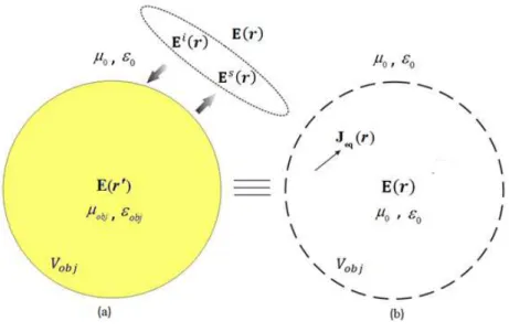
The general electromagnetic scattering problem is presented in Fig. 2a. The total electric fieldE
outside the volume Vobj of the nanoparticle is given by the sum of the incident plane wave and the
scattered from the nanoparticle wave:
i s
( ) ( ) ( ) ,
Er E r E r (2)
where superscripts i and s indicate the incident and scattered fields. The latter can be viewed as the
field radiated by an equivalent polarization current densityJeq( )r' , with
r
' objV
, as shown in Fig.2b. The scattered fields obey the Maxwell’s equations [19]:
s s
0
( ) (
jωμ )
E
r
Hr
(3)s s
0
( ) jωε ( ) ( ) .
H
r
Er
Jeqr
(4)The equivalent polarization current density Jeq( )r' exists only inside the material, and it is given by
0
[
( ) ( )
–
] ( ) ( ) ( )eq
J
r
' j
r
Er
'
r
Er
' , (5)where
r
'is the vector that indicates the source point, and0
( )r
ifr
obj
V
and
( )r
obj ifr
obj
V
. From(3) and (4) we obtain the wave equation2 0
( ) ( ) ( ),
s s
0 '
k
j
ωμ
E
r
E
r
Jeq r (6)where k0 ω μ ε0 0 2 / and the wavelength. The solution of (6) is given by s ( ) ( , ) ( ) obj 0 V
jωμ ' ' dv'
0 eqE
r
Gr r
Jr
,(7)
0
G is the dyadic Green’s function for free space defined by
0
1
, ,
( ) 2 0( )
0
' I g '
k
G r r r r (8)
, e 4
(
)
0 0 jk ' g ''
r r r rr r
(9)Equation (7) is used to calculate the scattered field outside the volume Vobj of the nanoparticle.
However, to calculate the scattered field inside the nanoparticle, where there is a singularity, one
should modify (7) according to [20]
s ( )
( ) ( , )
3 ( )
obj 0
V
PV ' ' dv'
j ωε
eqeq
J
E G J
r
r
r r
r
(10)where G( ,r r') jωμ0G0( ,r r'), PV means the principal value of the integral and the second term is
a correction factor. Substituting (10) in (2), we obtain the following integral equation
i ( )
( ) 1 ( ) ( , )
3 ( ) ( )
obj
0 V
τ
PV ' ' ' dv'
jωε τ
E r r E r r G r r Er . (11)
C. Solution by 3D MoM
This section presents a numerical solution of the integral equation (11) by 3D MoM. Firstly, we
write the integral equation (11) in scalar form given by
i
3
1
( )
( ) 1 ( ) ( ) ( ) , , 1, 2,3.
3 ( )
obj
p p p q
x x xq x x
0 V q
τ
E E PV ' E ' G ' dv' p = q
jωε
r
r r r r r r
(12)
In this equation, we set x = x1 , x = y2 andx = z3 . To solve the integral equation (12) by 3D MoM, we
divide the volume Vob j into N subvolumes Vm (m=1, …, N), where ( ) p x
E r and
( )
r
are constant ineach subvolume. With rmas the point in the center of this subvolume, applying (12) to each
n i 0 3 1 1 ( ) ( ) ( , 1 , 3j ) ( ) ( ) ( )
p p p q q
m
x x x x x
V N
m m n m n
q n
E E PV G ' dv' E
rr r r
r r r (13)
for p,q=1, 2, 3. The elements of
p q
mn x x
G are given by
2
0 2
0
, , 1, 2
, 1 , , 3 .
( ) ( )
p q 0
x x pq
q p
' g ' p q
G j
k x x
r r r r (14)
An equivalent representation for (13) is
3
1 1
( ) ( ), 1... , 1, 2, 3 .
p q q p
mn i
x x x n x m
N
q n
G E E m N p, q
r r (15)This equation can be written as [G][E]=–[Ei], where [G] is a matrix of order 3N×3N, while [E] and
[Ei] are vectors of dimension 3N. The elements of [G] are given by
0
1 ( )
3
( ) ( , )
p q p q obj
mn m
x x n x x m pq mn
V
G
j
PV G ' dv'
rr r r
(16)
where
pq 1 ifpq and
pq 0 ifpq ;mn 1if mn andmn 0 if mn.The total electric field at each point rmis determined by inverting the matrix [G]. The elements of
this matrix in (16) are calculated approximately by [19], [21]:
20 0 3
( ) ( )
1 (3 3 )
4
p q p q
mn n n mn mn mn
x x mn mn pq x x mn mn
mn
j k V exp j
G r j cos cos j (17)
formn ,and
0
0 0
3
0 0
2 ( ) ( )
[(1 ) ( ) 1] 1
3
p q nn x x pqn n
n n
G j jk a exp jk a
k j
r r
(18)
formn, where
1 , 2, 3
, m m m m x x xr
1, 2, 3 ,
n n n
n x x x
r ,
mn m n
R r r
0 ,
mn k Rmn
1/33 / 4 ,
Obviously, the higher the number of subvolumes N the better is approximation. The geometry of
the subvolumes Vn should be very close to a sphere of radiusan. However, good results can be
obtained using cubic cells as we show in this work.
After finding the electric field inside the volume Vobj, one can calculate the electric field anywhere
outside the nanoparticle by inversion of the system [G][E] = –[Ei]. To do this, we use the solution [E]
with (7) and (2) in points outside Vobj.
III. NUMERICAL RESULTS
Based on the theoretical model presented in the previous section, we develop an algorithm in C
language. To do this, we firstly define the constants and the variables of the problem. Then a 3D cubic
domain of height and length 4a is created, where a=60nm is the radius of the sphere. This spherical
volume is divided into cubic cells of dimensions dx=dy=dz. The spherical volume with radius a is
created in the point (x0, y0, z0)
2
2
20 0 0 .
xx yy zz a (19)
The central sphere is positioned at the origin of coordinate axis(x0 y0z0 0). For the case of the
nanorod, we create a rectangular volume with the length L =60nm and square cross section with the
size w =10nm. The axis of the nanorod is placed along the axis x, and it is centered at the origin of the
coordinate system.
The method does not require an Absorbing Boundary Conditions (ABCs) to simulate a free space
radiation because the Green’s function already takes into account the radiation condition. The ABCs
are used in other numerical methods, such as the FDTD or professional programs such as software
Comsol Multiphysics. The latter uses the Finite Element Method (FEM) and a special type of ABC,
known as perfectly matched layer (PML), or radiation condition, for an artificial absorption of
electromagnetic waves.
All the cells created inside the object are excited by a plane wave [Ei].Subsequently, the elements
of the matrix [ ] G 3N X 3Nare calculated for the volume of the object using (17) and (18) for
m
n
andm n
, respectively. The field inside the volume Vobj is obtained by the inversion of the linear systemin the form [E] = – 1
[ ]G [Ei]. This linear system is solved by the Gaussian elimination method for
complex numbers. Then we calculate the total field in any point outside the volume Vobj with (2) and
with the fields inside Vobj calculated in the previous step.
A. Nanosphere
Initially, for validation of the algorithm we compare our results with the classical solution for the
Comsol Multiphysics. Subsequently, also we analyze a rectangular nanorod to confirm the possibility
of implementing the algorithm for different geometries. All the simulations were realized in a core i7
computer with 16G of RAM.
The analyzed nanosphere has the radius a
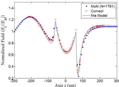
60nm. In this case, we use the total number of cubicelements N=1791 with the dimensions dx=dy=dz=8×10⁻⁹. The results of calculations for the near fields in the axis x, y and z are shown in Figs. 3-5.The amplitudes of these fields are normalized to the
magnitude of the incident plane wave Ei0. The electromagnetic wavelength used in all simulations is =550nm, which is near the resonance.
Fig.3. Normalized near field distribution for =550nm along axis x for gold sphere with radius a=60 nm.
Fig.5. Normalized near field distribution for =550nm along axis z for gold sphere with radius a=60 nm.
In Comsol simulation, we created a mesh of 131638 elements inside a spherical domain with
diameter D=460nm. The spherical domain is limited by a PML absorbing boundary condition to
simulate the open space. In Figs. 3-5, we observe a good agreement between the results for the used
discretizations. However, for the points near the surface of the sphere one can note a certain
difference in the results. This can be explained by rapid variation of the field in this region. This
means that we need a finer discretization in these regions to obtain a higher accuracy.
Fig.6 shows the variation of the x component of the normalized electric field versus wavelength for
different points along the axis x. The range of the analyzed wavelengths is between 500nm and
1000nm. The resonance of the sphere occurs near =550nm. The points where the electric fields were
calculated are positioned in (x=a+d, y=0, z=0), a is the radius of the sphere, and d runs through the
values 20nm, 40nm, 80nm and 160nm.
Fig. 6. Spectral response of normalized electric field (x component) near nanosphere in different points along axis x (x=a+d, y=0, z=0),
We observe from this figure a good agreement between the calculated results. For the points near the
sphere, electromagnetic fields vary rapidly with distance, therefore, it is necessary a finer
discretization of the nanosphere, as it was observed also in Figs. 3-5.
B. Rectangular Nanorod
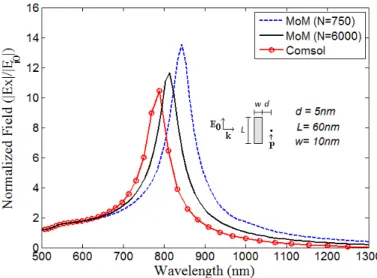
The analyzed rectangular nanorod has length L= 60nm, and width w =10nm. For this case, we
performed two simulations with different number of total cubic cells elements of the discretization N
to estimate convergence of the method. In one simulation, we used N=750, cubic cells of dimensions
dx=dy=dz=2×10⁻⁹, and in the other one we used N= 6000, with cubic cells of dimensions
dx=dy=dz=1×10⁻⁹. We also simulated this nanorod using Comsol software. In the latter case we used a mesh with 371747 elements, and a spherical domain limited by a PML. All the simulations were
realized in a core i7 computer with 16G of RAM.
We show in Fig. 7 the normalized electric field Ex at the end of nanorod at the point (x = L/ 2 +d, y
= 0, z = 0), where d =5nm and 20nm. Figs. 8-10 show the spectral response of the normalized electric
field in the axis z near the middle of the nanorod at the points (0,0, w / 2 +d), where w = 10nm is the
side of the square cross section of the nanorod (Fig. 1b), and d =5nm, 10nm and 20nm, respectively.
The wavelength interval extends from 500nm to 1300nm, where the principal resonances of the
nanorod occur.
Fig. 8. Spectral response of normalized electric field (x component) near middle of nanorod at point (x=0, y=0, z=w/2+d) with L = 60nm, w= 10nm, d = 5nm.
Fig. 9. Spectral response of normalized electric field (x component) near middle of nanorod at point (x=0, y=0, z=w/2+d), L = 60nm, w = 10nm, d=10nm.
We observe from Figs. 7-10 a good agreement between the MoM and Comsol Multiphysics results.
These figures show that with increase of N, our results converge to the Comsol simulation.
IV. CONCLUSIONS
We presented in this paper a 3D MoM computational algorithm for efficient full-wave
electromagnetic scattering analysis of plasmonic nanostructures. The method was codified in C
language, and two gold nanoparticles were analyzed: nanosphere and rectangular nanorod. To validate
the computational code, we compared our results with simulations carried out by the commercial
package Comsol. In case of nanosphere, we also compared the obtained results with the classical
analytical Mie model. In all cases, we observed a good agreement between the results obtained by our
code, the analytical model and the commercial software. We also analyzed convergence of the
method. For this purpose, we used different number of cubic cells N. For large values of N, our results
approach to the Comsol simulation. The full wave method is quite general and can be used to analyze
plasmonic nanostructures with different geometries and excitation sources. However, the method
requires a good computational capacity in terms of memory and processing speed.
ACKNOWLEDGMENT
This work was financially supported by the Amazon Foundation of Research of the State of Pará–
Fapespa - Brazil.
REFERENCES
[1] M. L. Brongersman and P. G. Kik, Surface Plasmon Nanophotonics, Netherlands: Springer, 2007. [2] L. Novotny, and B. Hecht, Principles of Nano-Optics, New York: Cambridge, 2006.
[3] N. C. Lindquist, et al, “Engineering metallic nanostructures for plasmonics and nanophotonics”, Rep. Prog. Phys., vol. 75, p. 036501, 2012.
[4] O. Sqalli, I. Utke, P. Hoffmann and F. M.-Weible, “Gold elliptical nanoantennas as probes for near field optical microscopy,” J. of Appl. Physics, vol. 92, pp. 1078-1083, July 2002.
[5] D. W. Pohl, “Near field optics as an antenna problem”', Near Field: Principles and Applications, The second Asia-Pacific Workshop on Near Field Optics, Beijing, China October 20-23, pp. 9-21, 1999.
[6] K. Q. Costa, and V. Dmitriev, “Analysis of modified bowtie nanoantennas in the excitation and emission regimes,” Prog. in Electro. Research B, vol. 32, p. 57-73, 2011.
[7] P. Bharadwaj, et. al., "Optical antennas", Adv. in Opt. and Photon., vol. 1, pp. 438-483, Aug. 2009. [8] L. Novotny and N. V. Hulst, "Antennas for light", Nature Photon., vol. 5, 2011.
[9] P. Biagioni, J.-S. Huang, and B. Hecht, “Nanoantennas for visible and infrared radiation”, Rep. Prog. Phys., vol. 75, p. 024402, 2012. [10] H. Wang, C. T. Chong and L. Shi, “Optical antennas and their potential applications to 10 terabit/in² recording,” Optical Data Storage
Topical Meeting, pp. 16-18, May 2009.
[11] T. A. El-Brolossy, T.Addallah, M.B. Mohamed, S. Abdallah, K. Easawi, S. Negm and H. Talaat, “Shape and size dependence of the surface plasmon resonance of gold nanoparticles studied by photoacoustic technique,” The European Physical Journal Special Topics, vol. 153, pp. 361-364, 2008.
[12] C. Hrelescu, T.K.Sau, A.L.Rogach, Frank Jackel and J. Feldmann, “Single gold nanostars enhance Raman scattering,” Applied Physics Letters, vol. 94, 153113, 2009.
[13] D. Cho, F. Wang, J. Valentine, Z. Yu, Y. Liu, X. Zhang and Y.R. Shen, “Plasmon Resonances of strongly coupled nanodisks,” Nano-Optoelectronics Workshop, pp. 88-89, 2007.
[14] V. Germain, A. Brioude, D. Ingert, and M. P. Pileni, “Silver nanodisks: size selection via centrifugation process and optical properties,” The Journal of Chemical Physics, vol. 122, 124707, 2005.
[15] W. Rechgerger, A. Hohenau, A. Leitner, J. R. Krenn, B. Lamprecht, F. R. Aussenegg, “Optical properties of two interacting gold nanoparticles,”Optics Communications, vol. 220, pp. 137-141, 2003.
[16] J. Neleyah, M. Kociaak, O. Sthepan, F. J. G. de Abajo, M. Tence, L. Henrard, D. Taverna, I. Pastoriza-Santos, L. M. Liz-Marza and C. Colliex, “Mapping surfaceplasmons on a single metallic nanoparticle,”Nature Physics, vol. 3, pp. 2248-353, 2007.
[17] D. E. Livesay, and K. M. Chen, “Electromagnetic fields induced inside arbitrary shaped biological bodies”, IEEE Trans. Micro. Theo. Tech., 22(12): pp. 1273-1280, 1974.
[18] J. A. Stratton, Electromagnetic Theory, New York: McGraw-Hill, 1941.
[19] C. A. Balanis, Advanced Engineering Electromagnetics,Jonh Wiley &Sons , pp.327-328, 1989.
[20] J. Van Bladel, “Some remarks on Grenns’s dyadic for infinite space,” IRE transactions on Antennas and Propagation, vol 9, pp. 563-566, 1991.