Advanced Control of Converters for
Fuel Cell Systems
Emil Benvindo Pereira Xavier
Mestrado Integrado em Engenharia Eletrotécnica e de Computadores Supervisor: Carlos João Rodrigues Costa Ramos
Devido às preocupações ambientais presentes nos últimos anos, o setor de energia tem tido um crescente interesse na pesquisa de fontes de energia renováveis e no desenvolvimento de sistemas de distribuição de energia. Para efetuar a ligação de sistemas de energia renovável à rede elétrica, é necessária a utilização de um conversor de potência para realizar a interface entre os dois.
O foco principal desta dissertação é fazer o estudo e implementação de uma estratégia de controlo avançado para um conversor de fonte de tensão, presente nos laboratórios da EFACEC. Este conversor fará a ligação entre um sistema de células de combustível e a rede eléctrica.
Este trabalho está estruturado em várias etapas, começando com um estudo dos conceitos relacionados, dos subsistemas envolvidos e das possíveis estratégias de controlo. Depois de uma caracterização detalhada do problema, a análise do sistema é feita de forma a compreender e desenvolver uma topologia de controlo para o conversor.
Uma vez que uma estratégia de controlo é proposta, foi criado um modelo de simulação para possibilitar o estudo do seu comportamento em termos de dinâmica, e qualidade da energia à sua saída, para poder assim avaliar o seu desempenho em regime permante e transitório.
Quando as exigências para as simulações foram todas cumpridas, procedeu-se ao projeto e construção de um protótipo do sistema, para confirmar os resultados obtidos nas simulações, em ambiente experimental.
Due to the environment concerns present in the last years, the power industry has taken an increas-ing interest on the research of renewable energy sources and the creation of DPGS’s. To make the connection of renewable energy systems to the electric grid, it is necessary to use a power converter to make the interface between them.
This dissertation main scope is to make the study and implementation of an advanced con-trol strategy for a voltage source converter present at the EFACEC company laboratories. This converter will serve as the interface between a fuel cell system and the electric grid.
The project is structured into several stages, starting with a background study of the related concepts, the involved subsystems and the control strategies.
After a detailed characterization of the problem, the system analysis is made in order to un-derstand and develop a control strategy for the converter.
Once the control design is proposed, a software simulation model was created to study its behavior in terms of its dynamics and power quality, making it possible to evaluate its performance on the steady state and transient operation modes.
When the simulations complied with all requirements, it was proceeded to elaborate the design and construction of a physical prototype of the system, to confirm the simulation results.
The realization of this dissertation could not be done without the help of the people who were always present when I needed.
First I would like to show my thanks to all my teachers, for the source of knowledge they have been, specially to my dissertation adviser, Carlos João Ramos, who were always available to help me and teach me during this period.
I would like to also thank all my friends, who have helped me through college, specially Luís Conceição, Nuno Tavares and Hugo Rocha.
Leave a very big thanks to my colleagues and friends from the Electrical and Computers Engi-neering department, who where very important and helpful on the development of this dissertation, namely Afonso Costa, Agostinho Rocha, Carlos Costa, Daniel Magalhães, Filipe Pereira, Justino Sousa and Vitor Sobrado.
Finally I would like to thank my family, specially my godmother Maria Jesus Silva Melo, for guiding me and giving me the possibility to take my studies this far.
To all, a great thank you.
Emil Benvindo Pereira Xavier
The author
1 Introduction 1 1.1 Objectives . . . 1 1.2 Planification . . . 2 1.3 Dissertation Structure . . . 3 2 State-of-the-art 5 2.1 Fuel Cell . . . 5
2.1.1 Components and its Functioning . . . 5
2.1.2 Fuel Cell Types . . . 6
2.2 Converter Topologies . . . 7
2.2.1 Voltage Source Converter . . . 8
2.2.2 Voltage Source Converter linked to a DC-DC Boost Converter . . . 10
2.2.3 Current Source Converter . . . 10
2.2.4 Multilevel Converter . . . 12 2.3 Grid-connected Filters . . . 13 2.3.1 L Filter . . . 13 2.3.2 LC Filter . . . 13 2.3.3 LCL Filter . . . 13 2.4 Synchronization Methods . . . 13 2.5 Modulation Techniques . . . 14 2.5.1 Sine-Wave Pulse-Width-Modulation . . . 15
2.5.2 Third Harmonic Injection Pulse-Width-Modulation . . . 16
2.5.3 Space Vector Pulse-Width-Modulation . . . 17
2.5.4 Triplen Harmonics Injection Pulse-Width-Modulation . . . 19
2.5.5 Flat Top Discontinuous Pulse-Width-Modulation . . . 20
2.6 Control Methods . . . 21
2.6.1 Proportional Integrator Control . . . 22
2.6.2 Proportional Resonant Control . . . 22
2.6.3 Vector Control . . . 23
2.6.4 Dead-beat Control . . . 23
2.6.5 Hysteresis Control . . . 24
2.6.6 Sliding-mode Control . . . 25
2.6.7 Fuzzy Logic Based Control . . . 25
3 System Analysis 27 3.1 Detailed Characterization of the Problem . . . 27
3.2 System Analysis . . . 28
3.2.1 Voltage Source Converter . . . 29
3.2.2 Grid Connection . . . 31 3.2.3 Synchronization Method . . . 33 3.2.4 Open-loop Control . . . 37 3.2.5 Performance Factors . . . 39 4 System Simulation 43 4.1 System Design . . . 43 4.1.1 L Filter Design . . . 44 4.2 Control Design . . . 45 4.3 Converter Control . . . 49 4.4 Simulation Results . . . 53 5 Physical Implementation 57 5.1 Control Platform . . . 58
5.2 Printed Circuit Boards Design . . . 60
5.2.1 Converter Printed Circuit Board Design . . . 60
5.2.2 Drive Printed Circuit Board Design . . . 62
5.2.3 Acquisition Printed Circuit Board Design . . . 64
5.2.4 Protection Printed Circuit Board Design . . . 65
6 Tests and Results 69 6.1 Acquistion Subsystem Test . . . 69
6.2 Drive Subsystem Test . . . 70
6.2.1 Dead Time Validation . . . 70
6.3 Protection Subsystem Test . . . 71
6.4 Synchronous Frame Phase-locked Loop Test . . . 73
7 Conclusions and Future Work 75 7.1 Future Work . . . 75
A Appendix 77 A.1 Printed Circuit Boards . . . 77
2.1 Basic components and the fuel cell way of function. [1] . . . 6
2.2 Fuel cell characteristic curve example. [2] . . . 7
2.3 Fuel cell based power system connected with the grid [3] . . . 7
2.4 Single-phase half-bridge converter (VSC) . . . 8
2.5 Single-phase DC-AC full-bridge converter. . . 9
2.6 Three-phase DC-AC converter. . . 10
2.7 Voltage source converter connected with a dc-dc boost converter . . . 10
2.8 Current source converter. . . 11
2.9 Current source converter with diodes connected in series with the IGBTs. . . 11
2.10 Multilevel VSC . . . 12
2.11 LCL filter placed between an VSC and the electric grid . . . 14
2.12 PLL functioning block diagram [4]. . . 14
2.13 Sine-wave modulation . . . 15
2.14 Fundamental waveform signal, Third Harmonic signal and resultant . . . 16
2.15 Phase-to-neutral voltage space vectors.[5] . . . 18
2.16 Branch voltages and space vector disposition for one switching period in sector 1.[5] 19 2.17 Fundamental waveform signal, Triplen Harmonic signal and resultant. . . 20
2.18 Fundamental waveform signal, Homopolar component signal and resultant. . . . 21
2.19 PI current controller. . . 22
2.20 PR control system structure. . . 23
2.21 Hysteresis current control. . . 24
2.22 Sliding-mode control system. . . 25
3.1 Fuel cell distributed generation system connected with the grid. . . 27
3.2 Voltage source converter with a LCL filter [6]. . . 28
3.3 Simulink model of the system with an open-loop control. . . 29
3.4 Voltage source converter without a neutral point. . . 30
3.5 Grid-tie converter. . . 32
3.6 Phasor connection between VSC and the grid. . . 32
3.7 MATLAB/Simulink SFR-PLL synchronization block. . . 34
3.8 Open-loop frequency response of the SRF-PLL. . . 36
3.9 Closed-loop frequency response of the SRF-PLL. . . 36
3.10 Open-loop current control block. . . 37
3.11 Modulation waves block. . . 38
3.12 Gate signals creation block. . . 38
3.13 VSC output currents. . . 39
4.1 Simulink’s High Power Circuit of th VSC. . . 43
4.2 Grid-connected converter equivalent circuit. . . 45
4.3 General control structure based on the dq reference frame (adapted from [7]). . . 48
4.4 Control simulation on MATALB/Simulink designed with Simulink’s library blocks. 49 4.5 Control simulation on MATALB/Simulink with only one code block. . . 50
4.6 Current control loop on the rotating d − q reference frame. . . 51
4.7 Current control loop. . . 52
4.8 L filter stability analysis. . . 52
4.9 Step response of the system with a L filter. . . 53
4.10 Measured grid currents for a constant reference value. . . 54
4.11 Measured grid currents for a reference change simulation. . . 54
4.12 Measured grid currents zoomed on a reference change. . . 55
4.13 Measured grid currents in the dq reference frame, idon top and iqon the bottom . 55 4.14 Control response analysis, id on top and iqat the bottom . . . 56
4.15 Measured grid current fast Fourier transform analysis. . . 56
5.1 Prototype system architecture. . . 57
5.2 MATLAB/Simulink control model for the DSP. . . 59
5.3 Diagram of the discrete time control. . . 60
5.4 OrCAD Capture voltage source converter circuit scheme. . . 62
5.5 OrCAD Capture drive circuit scheme. . . 63
5.6 OrCAD Capture drive circuit scheme. . . 64
5.7 Multisim model and simulation of the current sensor output conditioning. . . 65
5.8 Multisim model and simulation of the voltage sensor output conditioning. . . 65
5.9 OrCAD Capture acquisition circuit scheme. . . 66
5.10 SN54HTC flip-flop used on the protection circuit. . . 66
5.11 Multisim model of the designed alternating voltage protection circuit. . . 67
5.12 Alternating voltage protection circuit simulation output signals. . . 67
5.13 OrCAD Capture protection circuit scheme exert. . . 68
6.1 VabCH3 and VbcCH4 after conditioning. . . 70
6.2 Drive circuit input CH3 and output CH4. . . 70
6.3 Gate signals with turn-on and turn-off dead time. . . 71
6.4 Exceeding input signal CH3 and error signal CH2. . . 71
6.5 Input signal CH4 and error signal CH3. . . 72
6.6 Input signal CH3 and error signal CH2. . . 72
6.7 MATLAB/Simulink SF-PLL model for the DSP. . . 73
6.8 Theta angle CH4, acquired voltage CH3, generated voltage CH4. . . 74
A.1 OrCAD Layout voltage source converter printed circuit board. . . 77
A.2 Picture of the voltage source converter printed circuit board. . . 77
A.3 OrCAD Layout drive printed circuit board. . . 78
A.4 Picture of the drive printed circuit board. . . 78
A.5 OrCAD Layout acquisition printed circuit board . . . 78
A.6 Picture of the acquisition printed circuit board. . . 79
A.7 OrCAD Layout protection printed circuit board. . . 79
3.1 Converter possible states . . . 31
3.2 Current distortion Limits for GEneral Dist. Systems (120V - 69900V) [8] . . . . 40
3.3 System performance objectives. . . 42
4.1 System parameters. . . 43
4.2 Simulation parameters values . . . 52
4.3 Simulation parameters values . . . 53
5.1 IRG4PH50KD IGBT main characteristics. . . 61
AAFC Alcohol-air Fuel Cell AC Alternating Current
ADC Analog-to-Digital Converter ASD Adjustable Speed Drives CSC Current Source Converter DC Direct Current
DSP Digital Signal Processor
FACTS Flexible Ac Transmission Systems FFT Fast Fourier Transform
FPGA Field-programmable Gate Array GUI Graphic User Interface
MEA Membrane Electrode Assembly MCFC Molten Carbonate Fuel Cell PAFC Phosphoric Acid Fuel Cell PCS Power Conditioning Systems PCB Printed Circuit Board
PEMFC Proton Exchange Membrane Fuel Cell PI Proportional Integral
PLL Phase Locked Loop PR Proportional Resonant PWM Pulse Witdh Modulation RAM Random-acess Memory ROM Read-only Memory RMS Root Mean Square VSC Voltage Source Converter
WTHD Weighted Total Harmonic Distortion SMPS Switch Mode Power Supply
SOFC Solid Oxid Fuel Cell
SVPWM Space Vector Pulse Width Modulation THD Total Harmonic Distortion
TDD Total Current Demand Distortion UPS Uninterruptable Power Supplies
α Alpha A Ampere β Beta C Coulomb inf Infinite F Faraday γ Gamma H Henry Hz Hertz Ki Integral Gain Kp Proportional Gain µ Micro V Volt m Meters θ Theta t time W Watt
Introduction
The scope of this dissertation is the development of a control strategy for a converter that makes the interface between a fuel cell system and the the grid. The fuel cells are one of the renewable energy sources that can be used within the distributed energy systems. In the last years, these systems have been largely developed thanks to its advantages with the costs, more flexible production methods and less damage to the environment. Unlike the usual energy sources, renewable energy sources usually need an electronic converter that can interface them to the grid, so that the power flow can be monitored.
Since there can be changes on the grid performance, this converter must be able to accurately control the current flow and the grid voltage, so that it can quickly respond and adapt itself to these changes, otherwise, unwanted damages to the system components may occur.
1.1
Objectives
There are many important factors that can be considered on this dissertation but the focus will be the study, development and implementation of control algorithms, capable of guarantee the robustness, flexibility, speed, precision, reliability and security of the system. To keep this focus, the control algorithm has to achieve the follow objectives:
• Quickly and precisely monitoring of all the system variables; • Identify the grid changes influence on the VSC;
• Do the synchronization and control of these changes; • Give flexibility to the energy generation process; • Optimize the global performance of the system.
This algorithm must also be able to regulate the harmonic content on the system and adapt the converter operation to the parameter changes that come either from the AC side (grid) or DC side (fuel cell). In other words, the algorithm must do the advanced control of the system.
1.2
Planification
After looking at the objectives defined in the last section1.1, it is necessary to divide this project into different development stages:
• The bibliographic study of the literature related to the control algorithms/modulation tech-niques;
• The study of the most common VSC’s topologies and its operation characteristics; • The study of the best possible control methods to use on the dc-ac converters; • Create the model of the discussed fuel cell power generation system;
• The dc-ac voltage source converter simulation joined with synchronization method and a basic control method.
• Selection of a grid synchronization method;
• Selection of an open loop operation mode for the converter - Pulse Width Modulation type; • Selection of a basic current and voltage control method;
• The elaboration and simulation of a full bridge voltage source converter joined with an advanced control method;
• The study of the converter behavior in the presence of the grid parameters variation: fre-quency, voltage, harmonic content;
• The study of the converter behavior in the presence of the fuel cell parameters variation: current and voltage;
• The study and development of high performance controller in the presence of the distur-bances referred before;
• The implementation of the developed VSC control algorithm on a DSP based plataform; • Dissertation writing.
The mentioned simulations will be built on MATLAB/Simulink (control design) and PSIM (power circuit). The experiment validation will be done on a 4KVA prototype at FEUP’s depart-ment of electronic engineering laboratories. This prototype has a control card based on DSP’s.
1.3
Dissertation Structure
Beyond this introduction, this dissertation has 6 more chapters. Chapter2, has a brief introduction of the fuel cell and describes the state of the art of the dc-ac converter and the associated topologies. Chapter3has a detailed characterization of the problem and system analysis. Chapter4, addresses the system simulation with closed-loop control of the VSC. Chapter5, will present and explain the necessary steps for the creation of a prototype of the system. Chapter7, concludes the dissertation and shows the proposed future work.
State-of-the-art
2.1
Fuel Cell
An fuel is defined as a electrochemical device that continually converts chemical energy into electric power, as long as there are an oxidant and fuel to mix. Lately, these devices have been seen as a promising technology to face the ever growing power demand. The reason why, can be explained with its high efficiency on the power conversion with a low pollution factor [9]. These last years, the environment concern and the energy crisis stimulated more effort to research this technology. However, the vast application of these cells is still difficult due to its elevated costs, material limitation and small durability [1].
2.1.1 Components and its Functioning
A fuel cell is composed by three basic components: an anode, a cathode and an electrolyte between the two, better known as the membrane electrode assembly (MEA). Most of the used electrodes have a porous structure that increases the reactants transportation. The electrode material can be composed by a catalyst or a solid conductive matrix where the catalyst is deposited. The electrolyte is seen as the heart of the cell, it may exist either in the solid or liquid form and its constituent material depends on the fuel cell type [1].
Unlike batteries, fuel cells are able to keep its functioning just as long as the necessary reac-tants are given to it. Figure2.1, explains the way a fuel cell works. The fuel, that can be either hydrogen, methane, or methanol is supplied to the anode and the oxidant (oxygen or simply air) is supplied to the cathode. The fuel is catalytically oxidized at the anode, while the oxygen is cat-alytically reduced at the cathode. The electrons involved on the reaction between the fuel and the oxygen travel through an external circuit that goes from the anode to the cathode to create energy. The membrane is an electric isolator but it lets the ions (both protons from the anode or anions of oxygen from the cathode) migrate from one electrode to the other to complete the reaction and produce water. The lack of movement of the constituents of the cell let the maintenance of the cell be an easy job and its functioning be quite smooth [1].
Figure 2.1: Basic components and the fuel cell way of function. [1]
2.1.2 Fuel Cell Types
Nowadays there are five types of fuel cells that are being researched for industrial use: • PEMFC - based on the proton exchange on the fuel cell membrane;
• SOFC - solid oxide fuel cells; • MCFC - molten carbonate fuel cells; • PAFC - phosphoric acid fuel cells; • AFC - alkaline fuel cells.
Amongst these types, the PEMFC are being rapidly developed to be the first option for au-tonomous devices and applications linked to the electrical grid, thanks to its high power density, low temperature operation and its safe and simple structure. The most important PEMFC features are:
• Water production (as a residue);
• High efficiency when compared with thermal sources;
• Low temperature operation (up to 90oC), which allows fast startups;
• Usage of a solid polymer that minimizes the concerns with the construction, transportation and safety.
The stack characteristics are exposed through a polarization curve that shows the relation be-tween the terminal voltage and the current density.
The fuel cell voltage decreases almost linearly to the discharge current increase. To keep the polarization characteristics at a constant level, additional parameters like the temperature of the cell, air pressure, partial oxygen pressure and the membrane moisture have to be controlled as
Figure 2.2: Fuel cell characteristic curve example. [2]
well. A power system based on fuel cells consists of a fuel processing unit (reformer), a stack of cells and a power conditioning system (PCS) [3].
Figure 2.3: Fuel cell based power system connected with the grid [3]
2.2
Converter Topologies
The main objective of these power converters, also known as power inverters, is to generate alter-nate current at its output through a direct power source at its input, and they must allow the control of the power magnitude, frequency and phase [10].
The wave forms at the end of the VSC are needed for industrial applications like adjustable speed drives (ADSs), switch mode power supplies (SMPS), uninterruptible power supplies (UPS), flexible AC transmission system (FACTS), active filters and voltage compensators [10]. Beside these applications, these converters can also be used on renewable energy sources related applica-tions.
There are various topologies on the market but these are basically divided between these two: • Converters fed by a voltage source, (Voltage-Source Converter - VSC);
• Converters fed by a current source, (Current-Source Converter - CSC). 2.2.1 Voltage Source Converter
The VSC design has proven to be the most efficient on the industrial market, it also is the most reliable and has the fastest dynamic response. The totally integrated design of a VSC reduces costs, installation time, minimizes and or erases the power cables interrelation costs, thus lowering the necessary space amount for housing. Its levels of efficiency go up to 97% with a high power factor [11].
Within these type of converters, there are various topologies that will be shown next.
2.2.1.1 Single-phase DC-AC Converter
These converters can be of half-bridge or full-bridge topology. Even though they have a low power range, they are widely used on power supplies, single-phased UPS, and currently, they are also used to form more elaborated high power topologies like for example, the multilevel configurations [10] .
2.2.1.2 Single-phase Half-bridge DC-AC Converters
This topology (shown on figure2.4) is composed by two capacitors with the same capacity, where each one of these keeps the constant voltage of Vi
2, so that there is a neutral point between them.
The modulation techniques for this VSC must guarantee that the switches are never on at the same time, so that a short-circuit never happens. [3] The switches S+ and S- are alternately on, complementarily, at the desired output frequency. When the S+ is on, the S- is off and the output voltage is Vi
2, no matter the way the load current takes. Similarly, when S- is on and S+ is off, the
output voltage is −Vi
2. The voltage on the load is a square wave with a Vi
2 amplitude. For a resistive
load, the load current wave follows the voltage waveform. For an inductive load, the load current wave lags relatively to the voltage waveform, an angle approximately equal to the power factor angle at the load [12].
2.2.1.3 Single-phase DC-AC Full-bridge Converter
Figure2.5 shows the topology of a full-bridge VSC. This VSC is similar to the half-bridge one, although, there is a second branch that provides a neutral point on the load. As expected, the two switches S1+ and S1- (or S2+ and S2-) can never be on at the same time, otherwise there will be a short-circuit on the DC link. There are 4 defined states (states 1, 2, 3, and 4) and an undefined one (state 5). The undefined condition must be avoided so that the output AC voltage control can be controlled. The output alternate voltage can assume values that can achieve the DC value of the input voltage, that is two times superior to the one on the half-bridge topology. Various modulations techniques were developed for this VSC, amongst them are the PWM techniques (bipolar and uni-polar). [10]
Figure 2.5: Single-phase DC-AC full-bridge converter.
2.2.1.4 Three-phase DC-AC Converters
The purpose of this topology is to provide a three-phased voltage source, where the voltage am-plitude, phase and frequency can be controlled. This VSC can be identify as the connection of 3 half-bridge VSC’s in parallel with the same DC link. Like the half-bridge VSC’s, none of the switches that belong to the same branch can be switched on at the same time, otherwise, there will be a short-circuit [10]. The voltages in each branch are identical to the output voltages at the half-bridge and full-bridge circuits. The 3 square-wave voltages of the 3 branches of the VSC are shifted in time by a third of the output signal period [10].
This VSC can shift between 8 possible states, that allow it to generate the desired output waveform. The shift between the states is made by turning on and off the switches in each branch at the correct time. The selection of states is possible through the use of a modulation technique that must guarantee the use of viable states only. Merely this way, it can be possible to get an AC voltage waveform at the output, formed only by the input voltage values:Vi, 0, −Vi[10].
Figure 2.6: Three-phase DC-AC converter.
2.2.2 Voltage Source Converter linked to a DC-DC Boost Converter
If we choose a VSC fed by a voltage source to make the interface to the grid, the DC-link voltage may need to be boosted. This may be achieved with the use of an additional step-up converter like the one in the figure2.7. The input capacitor decouples the VSC and the converter, while it keeps the voltage ripple to an adequate level. One possible power flow control method for this system, can consist on the use of a step-up converter to keep the DC-link voltage at a constant value [2] .
Figure 2.7: Voltage source converter connected with a dc-dc boost converter
2.2.3 Current Source Converter
With a CSC converter topology, like its denomination indicates, the power is provided by a current source instead of a voltage source. With this type of converters, the switches are connected on a 6 state sequence to take the current to the load, with the desired waveform. The load and parallel capacitors commutation are two of the commutation methods for the CSC. In both methods, the input current regulation assists its functioning.
Figure 2.8: Current source converter.
The current source converters have found very low application until now, due to the wide utilization of voltage source converters. In fact, almost every implemented converter is of the VSC topology with only very few registered research publications about the CSC structures in the last years. Indeed, the converters of this type that have been designed, have been generally used with high power applications or parasite current handling at the motors windings [13].
Recent research on the area, have the focus of improving the performance and efficiency of this converters, with the study of alternative commutation methods that use a power commutation device, eliminating the necessity of commutation schemes, and implementing methods that can guarantee the dc current flow at the DC-link. The objective of this studies is to allow harmonic minimization techniques that are already used in VSC system, to be developed for CSC systems as well [13].
The current source converter increases the voltage through the current by itself, which means that the input voltage must be inferior to the lowest voltage value between phases, which elimi-nates the necessity of connecting a DC-DC step up converter. Similarly to what happens at the VSC systems that are connected with a step-up converter, the inductance at the DC-link keeps the current ripple at an acceptable value range. The used switches must have reverse blocking. If reg-ular IGBTs (insulated-gate bipolar transistor) are used , the reverse blocking can only be achieved through the use of diodes connected in series with them, as you can observe in figure2.9[13].
2.2.4 Multilevel Converter
In the last few years, several industrial applications began to require high power devices. This is due to the fact that there are some medium voltage units for motors and other applications that need power values that can go up to megawatts. At a medium voltage electric grid, directly connecting a semiconductor switch can be problematic, so, the multilevel systems were introduce as an alternative to these applications. A converter that has a lot of levels, not only achieves high ranges of power, as it also allows the use of renewable energy sources like the photo-voltaic power, wind power, and fuel cell. These sources may be easily connected to a multilevel converter in a system that operates at high power values [14].
A multilevel converter can switch its input nodes as well as its output nodes between multiple (more than 2) levels of voltage or current. Two level converters are not considered multilevel [15]. The traditional understanding of in what a multilevel converter consists follows this definition: One of the ports has multiple (more than two) voltage or current nodes or terminals, while the second port has one or three phases that are switched through several levels. Most of this type of converters use several levels of voltage. This configuration is generally the most useful for high power applications because it can reduce the conduction losses on both converters and machines, which makes it always preferable to use various voltage levels instead of various current levels [15].
Figure 2.10: Multilevel VSC
These converters structures place the switches in series so it can block the higher voltages [15]. For applications that involve high levels of current, several switches can be put in parallel with the current being summed by the inductors. Thus, when separately switched on, several levels current waveforms are created. [15]
2.3
Grid-connected Filters
Filters are a very important part of any converter that uses semiconductors because they can reduce the prejudicial effects of the switches commutation on the other system components [16], thus helping the system be in terms with the grid international standards.
These days, the PWM control is adopted in almost all the VSC’s, which results on a big presence of high order harmonics. These harmonics can flow to the grid, reducing this way, the quality of the signal and maybe even damage the equipment. To avoid this phenomenon, filters that can contain the harmonics were introduced at the end of the converters, thus reducing the pollution that goes to the electric grid [17].
2.3.1 L Filter
At the distributed generation systems, specially for some recent power generation devices, the first order low-pass filter L, is commonly used in grid-tie converters. In this area, when compared to the LCL filter, the L filter has notorious advantages that result from its simple design and no increase in the volume, weight and costs. [17] On the other hand, this filter is already a large one, somewhat inefficient and can not really take care of all the basic needs for the harmonic reduction on the electric grid.
2.3.2 LC Filter
The LC filters are second order systems that have been highly used at the end of DC-AC converters when the control object is the output voltage. As expected, the main objective of these filters is to attenuate the ripple caused by the commutation of the semiconductors, on the output signal [18].
The capacitor voltage of the filter is controlled by the converter control. These filters introduce an delay and cause resonance on the AC voltage. This is a problem, so there are being studied different approaches to regulate the capacitor voltage of the filter [18].
2.3.3 LCL Filter
On grid-tie voltage source converters applications, if a LCL filter is placed at the end of the VSC, the output signal can get really good quality.
When compared to the L filter, this filter can provide more flexibility on the way the VSC is used and can also give more ripple attenuation to the current that flows to the grid. In other words, it is more efficient. However, it can also bring resonance and instability to the system, which makes it necessary to design it accordingly to the specific parameters of the system.
2.4
Synchronization Methods
As it was mentioned before, the VSC has to be synchronized with the grid on its frequency, phase and magnitude so that it can be possible to generate a current reference signal. To make this
Figure 2.11: LCL filter placed between an VSC and the electric grid
synchronization on adverse conditions (distortion, perturbation and imbalances) is one of the main problems described on this type of systems literature. [13] To resolve this problem, there are studied synchronization techniques like the α-β filter and the PLL method (Phase Locked Loop). The article [19] suggests one new synchronization method for the parallel connection of two VSC’s to the grid, that generates energy for two distributed loads. However, on this dissertation, the PLL synchronization method will be used because it is most common on this type of systems. The PLL synchronization method must be robust and reliable against the electric grid vari-ations and the perturbvari-ations that are provoked by the harmonics, because if this block does not work correctly, the VSC control may be impracticable and consequently cause instability on the whole system. This method is composed by three blocks, one to make the phase detection, one that represents a low-pass filter and another one that represents an oscillator controlled by the voltage [20] .
Figure 2.12: PLL functioning block diagram [4].
2.5
Modulation Techniques
There are various control techniques for the VSC. The most efficient method consists in the in-corporation of a PWM based control. The PWM control technique is used to vary the RMS value of the AC side waveform. This technique can also improve the harmonic content of the currents,
taking the voltage harmonics to higher frequencies and by doing this, it simplifies its filtering. This technique consists on controlling the output mean value during a given period with pulses that have a duration that is proportional to the desired mean value. There are various types of pulse-width modulations. Next there are going to be reviewed the most used ones.
2.5.1 Sine-Wave Pulse-Width-Modulation
The objective of this modulation is to create various pulses with different durations, and to achieve this, a triangle-wave (carrier signal) c(t) with a ft frequency and Vt amplitude is compared with
three sine-waves (modulation signals) with a fm frequency, Vm amplitude, βmphase, and with a
120ophase difference between each one of them:
mk(t) = macos(2π fmt+ βm− (k − 1)
2π
3 ), k = 1, 2, 3 (2.1) The modulation index is defined as:
ma=
Vm
Vt
(2.2)
The frequency index is defined as:
mf =
ft
fm
(2.3) To simplify the equation, the Vt is considered as unitary:
mk(t) = Vmcos(2π fmt+ βm− (k − 1)
2π
3 ), k = 1, 2, 3 (2.4) And the switches gate commands are defined as:
gk(t) =
(
1 if mk(t) ≥ c(t)
0 if mk(t) < c(t)
k= 1, 2, 3
In the linear zone, the phase to phase RMS voltage Vppvalue, varies linearly with the ma, for
ma values between 0 and 1. In this zone, harmonics only appear at higher frequencies that are
multiples of the commutation frequency. In this zone, the Vcvaries linearly with the mavalue:
Vc=
√ 3
2√2Vdcma , ma= 0..1 (2.5)
When the mavalues gets bigger than 1, this technique enters into a non-linear zone where low
frequency harmonics appear. In this zone, the Vppvalue increases less and less with the mavalue
increase. At the limit, when ma tends to infinity, the AC voltage of the VSC controlled by this
technique becomes equal to the AC voltage of the VSC controlled by a square-wave modulation technique [21].
2.5.2 Third Harmonic Injection Pulse-Width-Modulation
The Third Harmonic Injection PWM (THI-PWM) is a modification over the Sine-Wave PWM (SPWM) briefly revised on the section2.5.1. This technique consists of adding to the sinusoidal modulating signal of fundamental frequency, the necessary amount of third harmonic signal. Then the resultant modified waveform is compared with the high frequency triangular carrier waveform. The comparator output is used for controlling the inverter switches in the same manner as the SPWM technique. [22]
Figure 2.14: Fundamental waveform signal, Third Harmonic signal and resultant
In other words, if a fundamental frequency signal is having a peak magnitude slightly higher than the peak magnitude of the carrier signal, a suitable amount of 3rd harmonic signal is mixed with it, so the modulation signal does not go out of the linear zone and makes the correct control of the three-phase converter. [22] [21]
mk(t) = ma(cos(2π fmt+ β − (k − 1)
2π 3 ) +
1
With this technique it is possible to elevate the linear zone of the modulation up to the maxi-mum modulation index, equal to:
ma=
2√3
3 = 1.15470 (2.7)
To this mavalue, the maximum mk(t) value is the unity.
The rms value of the phase-to-phase voltages will continue to be derived from the2.5equation but the maximum limit of mawill alter to value on2.7.
The maximum Vc value that it is possible to obtain through this modulation technique in the
linear zone is given by:
Vcmax= √ 2 2 Vdc' 0.707107Vdc, with ma= 2√3 3 (2.8)
Which means that this homopolar component addition allows to get a higher profitability from the DC-link than the SPWM does, in the order of approximately 15, 47%. [21]
2.5.3 Space Vector Pulse-Width-Modulation
This technique offers significant advantages over the regular sampled sinusoidal PWM. The major advantages include its high performance in terms of better harmonic spectra, ease of implemen-tation and enhanced DC-link utilization. This technique is based on the represenimplemen-tation of the three-phase converter. The output voltages is defined as:
vs= 2 3(va+ avb+ a 2v c) (2.9) Where a = ej2π3 and a2= ej4π3 .
This variable is a complex variable and is in function of time in contrast to the phasor. As said before on the section 2.2.1.4, the VSC generate eight switching states which include six active and two zero states. These vectors form a hexagon2.15which can be seen as consisting of six sectors spanning 60% each. The reference vector which represents three-phase sinusoidal voltage is synthesized using SVPWM by switching between two nearest active vectors and zero vector. [5]
The binary numbers on the figure2.15indicate the switch state of the converter branch. Where, 1 implies upper switch being on and 0 refers to lower sitch of the branch being on. The most significant bit is for the first branch after the dc bus, the bit on the middle is related to the middle branch and the least significant bit is related to the last branch.[5]
Figure 2.15: Phase-to-neutral voltage space vectors.[5]
The time of application of active space voltage vectors (as in sector 1 of figure2.15) is found as: ta= | V∗ s | | va| sin(π 3− α) sin(2π3 ) tb= | V∗ s | | vb| sin(α) sin(2π3) t0= ts− ta− tb (2.10)
where | va |= vb= 23Vdcv∗s is the reference vector magnitude, α is the angle or position of
reference vector and ta, tb and t0 are time of applications of vector va, vector vb and zero vectors
respectively. In order to obtain fixed switching frequency and optimum harmonic performance from SVPWM, each branch should change its state only once in one switching period. The next half of switching period is the mirror image of the first half. The total switching period is thus divided into seven parts, the zero vector is applied for one-fourth of the total zero vector time first followed by the application of the active vectors for half of their application times and then again zero vector is applied for one-fourth of the zero vector time. This is then repeated in the next half of the switching period and this is how symmetrical SVPWM is obtained. The branch voltages in one switching period are depicted in figure2.16for sector 1.
The sinusoidal reference space vector form a circular trajectory inside the hexagon. The largest output voltage magnitude that can be achieved using SVPWM is the radius of the largest circle that can be inscribed within the hexagon. This circle is tangential to the mid points of the lines joining the ends of the active space vector. Thus the maximum obtainable fundamental output voltage is
Figure 2.16: Branch voltages and space vector disposition for one switching period in sector 1.[5] [5]. v∗ s = 2 3Vdccos( π 6) = 1 √ 3Vdc (2.11)
2.5.4 Triplen Harmonics Injection Pulse-Width-Modulation
The objective of this type of modulation technique is to lower the absolute value of the three modulation waves at every instant. This modulation has the same properties of the space vector pulse-width-modulation technique. [21]
The original modulation waveforms, as seen before, are given by:
mk(t) = Vmcos(2π fmt+ βm− (k − 1)
2π
3 ), k= 1, 2, 3 (2.12) The homopolar component that is added to the modulation waveforms are given by:
mh(t) =
−1
2 (max(mk(t), k= 1, 2, 3) + min(mk(t), k= 1, 2, 3)) (2.13) resulting on a waveform very similar to the triangular waveform with a frequency three times higher than the modulation waveforms frequency.
The decomposition of the mhin spectral components is given by [21]:
mh(t) = ma √ 3π ∞
∑
n=0 (−1)n ((2n + 1) −13)((2n + 1) +13)sin(3(2n + 1)(2π fmt+ βm)) (2.14) The final modulation waveforms are given by:m0k= macos(2π fmt+ βm− (k − 1)
2π
Figure 2.17: Fundamental waveform signal, Triplen Harmonic signal and resultant.
At a computational level it is more efficient to obtain the duty cycles directly from the2.12
equation, and then apply to it a discrete equation equivalent to the2.13. With this procedure, it is obtained: δk[n] = macos(2π fmTcn+ βm− (k − 1) 2π 3 + π fmTc), k= 1, 2, 3, δh[n] = −1 2 (max(δk[n], k = 1, 2, 3) + min(δk[n], k = 1, 2, 3)), δ 0 k[n] = δk[n] + δh[n], k= 1, 2, 3 (2.16)
2.5.5 Flat Top Discontinuous Pulse-Width-Modulation
The objective of this technique is to minimize the number of switch commutations, reducing this way the energy losses inherent due to them. This modulation is entitled discontinuous because the homopolar component that is summed to the carrier waveforms it is represented by a discontinuous time function. [21]
Since there are six switches on the VSC, the commutations and the conduction time is equally distributed by each one of them, and each period of the modulation waveforms is divided in six parts. In each part, one of the switches is kept on and the other switch from the same branch is kept off. This way, the effect of the injected homopolar component makes the modulation waveform saturate (on the value 1 or -1) on the zone where the respective switches are always on. [21]
The original modulation waves are give by:
mk(t) = macos(2π fmt+ βm− (k − 1)
2π
3 ), k= 1, 2, 3 (2.17) and the homopolar component is defined by:
mh(t) = −(m2(t) + 1), if m2(t) = −max(| mk(t), k= {1, 2, 3} |) (m1(t) − 1), if m1(t) = max(| mk(t), k= {1, 2, 3} |) −(m3(t) + 1), if m3(t) = −max(| mk(t), k= {1, 2, 3} |) (m2(t) − 1), if m2(t) = max(| mk(t), k= {1, 2, 3} |) −(m1(t) + 1), if m1(t) = −max(| mk(t), k= {1, 2, 3} |) (m3(t) − 1), if m3(t) = max(| mk(t), k= {1, 2, 3} |)
resulting in the final modulation waves:
m0k= macos(2π fmβm− (k − 1)
2π
3 ) + mh(t), k= 1, 2, 3 (2.18) Figure 2.18 shows one of the possible implementations of this technique. There it can be observed the saturation principle of the modulation signal: between the angles 60◦ and 120◦ the phase is kept at the high level and the switch S1is kept on, and between the angles 240◦and 300◦,
the same switch is kept at the low level and is off. [23]
Figure 2.18: Fundamental waveform signal, Homopolar component signal and resultant.
2.6
Control Methods
The control technologies for VSC’s can be divided into two groups. The first one is the linear control which includes the proportional integrator controller (PI), the proportional resonant con-troller (PR), the vector control or d-q transform (direct-quadrature), the dead-beat concon-troller and the sliding-mode controller. The other group is the non-linear control where it can found the hys-teresis control and the fuzzy control [9]. A brief introduction to each one of these control methods
will be made next and a more profound approach will be done to the chosen one, further ahead on the chapter5.
2.6.1 Proportional Integrator Control
This is the most common controller since the 80s [9]. This method produces a command voltage through a PI compensator. The integral part minimizes the error at low frequencies and the pro-portional part is related to the output current ripple. This is a very easy controller to use but there are some very well known disadvantages related to the use of this method: the inability to follow the output currents sinusoidal reference with a null error and the weak perturbation rejection ca-pability. Thus, when the attenuation and the resonant frequency of the filter varies in significantly way, the controller becomes unstable for the system. To solve this problem, feed-foward PI current controller with two loops can be introduced but, in despite of that, these controllers have a weak dynamic response and continue to have a low perturbation rejection capability [24].
Figure 2.19: PI current controller.
This control method is normally used with other control methods at the same time, for exam-ple, the dead-beat control [9].
2.6.2 Proportional Resonant Control
This controller has been proposed in more recent projects, where it has shown a superior perfor-mance than the PI controller, where it finds its basis. It works with very high gains for the desired frequencies (resonant frequencies) so it can reduce the steady state error and avoid introducing lag to the control loop at the same resonant frequencies, resulting in a harmonic minimization on the VSC and the reduction of the output current distortion [25]. In other words, it is able to effectively follow a reference signal.
Article [25], refers that the implementation of this control method, when compared to the conventional methods, brings the follow advantages:
• It has no error for sinusoidal wave-forms with fundamental frequency (grid frequency). This ability can be explored for the harmonic compensation where the signal frequencies are well defined and always constant;
• This controller acts as an active resonant filter for fundamental frequencies. This way, many PR controllers can operate in parallel without interfering with each other.
The proportional part acts the same way the PI controller proportional part does, and it basi-cally determines the system dynamics in terms of bandwidth, phase and margin gain. The integral part only activates to vertically change the response magnitude [25].
Figure 2.20: PR control system structure.
Article [25] also explains that in theory, there is undefined gain in an ideal PR controller at the fundamental frequency, which allows the steady state error extinction without any gain or phase changes at other frequencies. On the other hand, this undefined gain can bring a series of problems to the system stability. To solve this, a non ideal controller must be used. This controller presents a finite gain that is big enough to erase small steady state errors and keep a good performance for the desired harmonics.
2.6.3 Vector Control
This type of control method is distinct because of its capability to obtain excellent precision and good performance. Some other characteristics include the possibility to control the signal error like its a regulated dc value. This control also permits the use of a classic PI controller to achieve infinite gains to determine the duty-cycle through the value transformation.
Article [26] presents a current controller for a single-phase grid connected VSC that allows the independent control of the active and reactive components of the power that flows to the grid. This method makes a vector transformation from the α-β stationary plan, to the d-q rotational plan of an orthogonal pair that consists of the VSC output current and modified time version of that current.
Nonetheless, this control scheme is not perfect because it needs more time to compute. This can turn up to be a very unpleasant problem when designing and implementing this method [9].
2.6.4 Dead-beat Control
This is a feedback controller with a very fast dynamic response which is the reason why its usage is very common amongst active power filters and high performance ASDs [9]. Its characteristics include high output signal controlling capacity, short response time, short adaptation time and null steady state error.
In discrete time theory, the dead-beat control consist in finding the input signal that must be applied to the system so it stabilizes the output with the least number of time-steps. For N order linear systems, it can be verified that the least number of steps it is going to be N at most (depending on the initial condition), just as long as the system can be taken to the initial state by an input signal. For non-linear systems, this method is still a research target because it still has aspects that can be improved [27].
Article [27] refers that the dead-beat control of three-phase VSC’s has been amply researched in last years, specially for drive related applications. The application of this technique to active filters is almost direct, however, the effect of the filters (that are commonly used to eliminate high order harmonics derived by the VSC’s modulation) at its input must be very carefully analyzed. In reality, these filters are not normally taken into account in the design of this controller and the current behavior changes with its presence and may become unstable.
This same article also discusses the problems that are related with the difference between the parameters used in the model design and the real values that are used in its physical implementa-tion.
2.6.5 Hysteresis Control
The hysteresis current control is one of the easiest methods to apply. Its use is simple and it is robust against load parameters changes. This method controls the VSC through a continue comparison between the current and its reference. From this comparison results in a error signal that is directly compared with a predefined band, which is called the hysteresis-band, the result of this comparison produces a pulse modulation signal that is used to asynchronously control the VSC semiconductors [28].
Figure 2.21: Hysteresis current control.
These controllers are vastly used thanks to its simplicity, robustnes and dynamics but still has disadvantages when it comes to the commutation frequency which is variable due to the fixed hysteresis-band. This limitation is a big problem to the VSC’s control, because it compromises the output filter design. This disadvantage can be supressed if other methods are used at the same time, like it is discussed in the article [9].
2.6.6 Sliding-mode Control
This method was proposed for power conditioning systems based on a variable control structure. Lately, this control is being attracting more attention to it because of its excellent performance. The designing of this control can be resumed into two parts: selecting the sliding surface Si(x) and
find the control laws Ui±. The objective of this controller when used on a grid-tie VSC is to make
the output currents follow its reference with the maximum precision. This basically resumes itself as a movement tracking problem [29].
Article [29] shows that for a three-phase system, there are only two independent sliding surface equations. According to this method arrival condition, we can conclude that S ˙S<0 and with this condition, the control laws can be found.
Figure 2.22: Sliding-mode control system.
The control process consists of comparing the measured current with its reference, that must be synchronized with the grid (same frequency and phase), then, the obtained errors are sent to the sliding-mode controller, which creates a pulse modulation signal that activates or deactivates the VSC switches.
2.6.7 Fuzzy Logic Based Control
Fuzzy logic controllers can obtain conclusions from systems that have confusing or imprecise characteristics, they can achieve this through the creation of fundamental rules with linguistic variables of the system and by trying to coherently adapt it to a defined end.
The fuzzy logic control is an alternative to a vast variety of control methodologies since it can provide a convenient method to elaborate a non-linear control system based in heuristic processes. A fuzzy control consists in rule base, fuzzification, inference mechanism, and difuzzification. The rule base receives the control rules that describe the advanced knowledge of a fuzzy structure. In the fuzzification process, the numeric values of the signal are converted to a fuzzy language. After that, through the converted values, a established data base and a control language, it is possible to generate values from an inference mechanism. Since the generated values will still be in the fuzzy
language, it is necessary to convert them back to numeric values through a difuzzification process [30].
System Analysis
3.1
Detailed Characterization of the Problem
The work proposal for this dissertation will focus (as it was referred in the beginning of this document) on the study and development of an advanced control for an electronic converter that will serve as the interface between a fuel cell system and the electric grid. This converter must be synchronized with the grid in terms of phase, magnitude and frequency and it must be capable of rapidly respond to the grid parameters variations. If the converter does not do this task effectively, the grid power may return to the system and damage the equipment, including the cells. Because of this, it is crucial that these systems have very efficient, reliable and safe interfaces.
Figure 3.1: Fuel cell distributed generation system connected with the grid.
The most common topology for this type of systems is the DC-AC voltage source converter (VSC) with two pulse width modulation levels, like the one in the figure3.2[6]. This topology is the state-of-the-art for these applications and was chosen to implement the physical process model that needs to be developed/researched on this dissertation.
This VSC topology has several possibilities in respects to its functionality. This flexibility is due to its fast response [6]. While VSC’s that are not connected with the grid, control the output voltage, a VSC that is connected with the grid, controls the output current with respect to the grid voltage, so it can transfer the energy to grid with a unitary power factor. The control algorithm of these VSC’s can vary in accordance with the current sensor point in the inductor and the grid or the voltage sensor point in the capacitor filter and the grid [9].
Figure 3.2: Voltage source converter with a LCL filter [6].
As explained before, the PWM control of the VSC’s, can result in a big harmonic presence that may take away the signal quality and may be harmful to the equipment of the system. To solve this problem, there is a need to use filters that can contain those harmonics, working as an interface between the VSC’s and the grid. These filters may be constituted by one inductor only (L filter), a capacitor or an inductor based configuration or even a LCL filter. This last one is the most common choice but on this dissertation, there will be used the L filter.
The LCL filter is a third order system that introduces a vastly superior harmonic attenuation when low value inductances are used. However, it has a problem related with the existence of a resonance frequency, which originates extremely high currents, even in the presence of residual voltages at this frequency. The controller of a converter that has a LCL filter needs to have a way of compensating and cancel this resonance frequency effect, which will make it a more complex controller than the one for the L filter.
For this system to work according the defined objectives, it is necessary to control the current that goes to the grid according to a reference guideline for the active current and the grid phase, imposing the voltage generated by the converter on the AC side. To make this happen, a synchro-nization block that gets the angle position reference is need, so that the output voltage has the same phase as the grid voltage. After this, there is also a need to make a controller for the DC-link voltage, that can generate an active current reference according to the voltage error.
In conclusion, the VSC must possess and current controller that guarantees safety and at the same time signal quality for the electric grid, in other words, with an almost nonexistent error in steady state, with a very low harmonic effect on the currents, a strong perturbation rejection capability and dynamic and fast response.
3.2
System Analysis
In this section, first it is going to be presented an explanation of how the VSC operates through the analysis of the currents and voltage related to the gate signals. After this, it is going to be presented
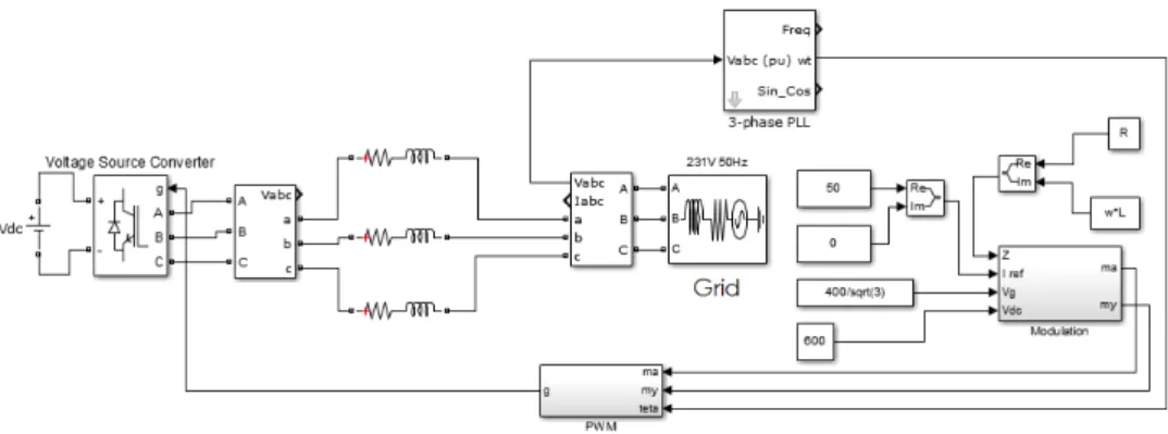
the grid connected operation mode of the VSC. Then it is explained how to create the gate signals through the chosen modulation technique and why the need for a synchronization method. In order to better understand its functioning, it is going to be made the open-loop control of the alternate currents of a grid-tie VSC (working as an inverter). To do this, a MATLAB/Simulink model of the system was designed with a PWM control, designed to follow a given current reference3.3. After this simulation, it is going to be defined the performance factors for the system evaluation.
Figure 3.3: Simulink model of the system with an open-loop control.
3.2.1 Voltage Source Converter
As said before in the chapter2, section2.2, the two level three-phase converter makes the power transfer between a DC voltage system and an AC voltage system, and it can work with varying voltage magnitude and frequency. The energy can flow both ways, when the power flows from the AC side to the DC side, the converter is working as a rectifier, and when the power flows from the DC side to the AC side (normally the grid), the converter is working as an inverter.
This converter has two variants: with or without a neutral point. Their use depends on whether if the AC side has a neutral point or not and depends on the DC side need for a medium point. Figure3.4shows the variant that does not have a neutral point and this is the one that is going to be used on this chapter. There are no currents in the neutral point so the homopolar components of the voltages do not originate currents. This property is taken in advantage by the PWM command systems to elevate the AC voltage that the converter is able to generate, in comparison to the voltage that can be generated by the variant that has a neutral point [21] .
Since there is no current on the neutral point with this type of converter, the currents of the three phases will not be independent from each other. In this case, the currents vary only with the voltages between phases, which relate with the gate signals by the following manner:
v12= (g1− g2)vdc
v23= (g2− g3)vdc
v31= (g3− g1)vdc
Figure 3.4: Voltage source converter without a neutral point.
And the currents relate to the gate signals in this way:
idc= g1i1+ g2i2+ g3i3 (3.2)
This means that we have three control variables g1, g2 and g3 to control only two variables
(ex: v12and v23). This circumstance can be taken into advantage to improve the control technique
[21].
Even though the neutral point is not accessible, it is still important to deduct the phase to neutral voltages assuming that the converter is connected with a balanced load in the AC side. The equations that describe the AC side of the systems in this situation are given by:
v12= i1Z− i2Z
v23= i2Z− i3Z
0 = i1+ i2+ i3
(3.3)
After defining the vknas the k phase to the virtual neutral point n (created by a balanced load)
voltage, it is possible to determine the following equations:
v1n= 2v12+ v23 3 v2n= −v12+ v23 3 v3n= −v12+ 2v23 3 (3.4)
v1n= (+ 2 3g1− 1 3g2− 1 3g3)Vdc v2n= (− 1 3g1+ 2 3g2− 1 3g3)Vdc v1n= (−1 3g1− 1 3g2+ 2 3g3)Vdc (3.5)
The voltage between the virtual neutral point and the medium point of the DC-link is deter-mined by the following expression:
Vn0= (
1
3(g1+ g2+ g3) − 1
2)Vdc (3.6)
The eight possible states, resulting from the combination of the gate signals are represented in the table.3.1
Table 3.1: Converter possible states
g1 g2 g3 v12 v23 v1n v2n vn0 0 0 0 0 0 0 0 −12vdc 0 0 1 0 −vdc −13vdc −13vdc −16vdc 0 1 0 −vdc +vdc −13vdc +12vdc −16vdc 0 1 1 −vdc 0 −23vdc +13vdc +16vdc 1 0 0 +vdc 0 +23vdc −13vdc −16vdc 1 0 1 +vdc −vdc +13vdc −23vdc +16vdc 1 1 0 0 +vdc +13vdc +13vdc +16vdc 1 1 1 0 0 0 0 +12vdc 3.2.2 Grid Connection
When we connect the VSC to the electric grid, the impedance seen from the VSC side, must be inductive or else a short-circuit is made. If the connection point does not have enough inductance to limit and filter the current, more inductance must be added between the VSC and the connection point.
Figure3.5shows a representation of a grid-tie converter. The resistors that are in series with the inductance represent the inherent resistances of the connections and the devices in the system. The phasor connection between the VSC and the grid is represented in the figure3.6:
With this representation, the voltages, currents, impedance and power are exposed as complex numbers:
Vg= Vg (3.7)
Vc= Vcr+ jV i
Figure 3.5: Grid-tie converter.
Figure 3.6: Phasor connection between VSC and the grid.
i= ir+ jii= iejα (3.9)
S= P + jQ = Sejα (3.10)
Z= R + jωL = Zejα (3.11)
φ = arctan(ω L
R ) (3.12)
The PWM commands vary with two parameters, the modulation index (ma) and the phase (α),
which leaves to the following voltage expressions: Vc= kVdcmaejα Vcr= kVdcmacos(α) ma= [0, mamax] , α = [−π , π ] Vci= kVdcmasin(α)
The k and mamaxvalues depend of the type of modulation, and for the sine-triangle modulation, they are: k= √ 3 2√2 , mamax= 1 (3.13)
The current that goes from the converter to the grid is given by:
i=Vc−Vg Z (3.14) ( ir=ZR2V r c +ω LZ2V i c− R Z2Vg ii=ω L Z2V r c +ZR2V i c−ω LZ2Vg ( ir=ZkVdcmacos(α − φ ) −ZR2Vg ii=ZkVdcmasin(α − φ ) −ω LZ2Vg
And the active and reactive power that goes to the grid are given by the following equations:
Pc+ jQc= Vci∗ (3.15) ( Pc=ZR2(V r2 c +Vi 2 c ) − Vg Z2(RV r c − ωLVci) Qc=ω LZ2(V r2 c +Vi 2 c ) − Vg Z2(ωLV r c − RVci) ( Pc= −ZkVgVdcmacos(α + φ ) + k2RVdc2m2a Z2 Qc= −ZkVgVdcmacos(α + φ ) + k2ω LV2 dcm2a Z2 3.2.3 Synchronization Method
As said in the2-2.4, and as it could have been understood in the last section3.2.2, when dealing with the control of grid connected converters, there is a need to make the correct generation of the reference signals through a fast and accurate detection of the phase angle, the grid frequency and voltage amplitude. This need comes from the possible non-idialities in the power system that can originate disturbances like a phase difference between the grid current and its reference, because of the current loop controller parameter’s effect, the inverter filter inductor and the measured phase error of the grid voltage. The referred phase difference makes the electric grid absorb active power as well as reactive power, which can create undesirable effects on the electrical equipment such as resonances, increasing power losses, pre-mature aging and security risks. [31]
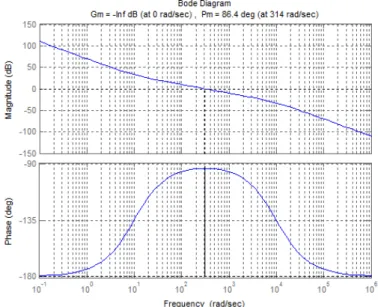
The PLL (Phase-Locked-Loop) method is an effective control method to solve this problem. The PLL can be defined as an algorithm that determines a signal to track another, so that the output signal is synchronized with the input one both in frequency and in phase. On this dissertation simulations, it is going to be build a SRF-PLL (Synchronous Reference Frame) block, that can be seen in the figure3.7.
Figure 3.7: MATLAB/Simulink SFR-PLL synchronization block.
Synchronous Frame PLL (SF-PLL) is widely used in three-phase systems. The instantaneous phase angle θ is detected by synchronizing the PLL rotating reference frame to the utility voltage vector. The PI controller sets the direct or quadrature axis reference voltage Vdor Vqto zero, which
results in the reference being locked to the utility voltage vector phase angle. In addition, the voltage frequency and amplitude can be obtained as the byproducts. Under ideal utility conditions without any harmonic distortions or unbalance, SRF-PLL with a high bandwidth can yield a fast and precise detection of the phase and amplitude of the utility voltage vector. In case the utility voltage is distorted with high-order harmonics, the SRF-PLL can still operate if its bandwidth is reduced at the cost of the PLL response speed reduction in order to reject and cancel out the effect of these harmonics on the output. [32]
For this dissertation, the grid voltage vector synchronization is defined with the direct compo-nent. The transformation to the dq rotating reference frame, is given by:
" Vd Vq # =2 3∗ "
cos(θ ) cos(θ − γ) cos(θ + γ) − sin(θ ) − sin(θ − γ) − sin(θ + γ)
# ∗ Va Vb Vc (3.16)
Where γ =2π3 and θ is the estimated phase angle, which is the synchronization block output. The quadrature voltage Vq is regulated to zero through the synchronous referential and when the
error becomes zero, it means that the synchronous referential is rotating at the same frequency of the grid.
The purpose of the feedforward frequency 2π f = 100π, is to have a proportional integrator control output signal that can be regulated to zero on a steady state operation mode. In the ideal case, when the grid frequency is exactly 50Hz and the regulator has tracked the phase, its output is zero. [33]
Since this application will be working in a sampled system, it is necessary to take the delay effect into consideration. This means that the transfer function for the plant will be a lag and an
integrating element. [33]
G(s) = ( 1 1 + sTs
)(1
s) (3.17)
For the design of the PI regulator was chosen the Symmetrical Optimum method, which use is indicated to systems where the plant can be described through the following transfer function:
H(s) = 1 s(
K
1 + sT) (3.18)
which is the case.
The parameterization of the PI controller that results from the H(s) transfer function is given by: Kp= 1 aKT Ti= a2 T a= 1 wcT (3.19)
where wcis the cross-over frequency.
Using the variables of the actual system plant we get:
Kp= 1 aV Ts Ti= a2 Ts a= 1 wcTs (3.20)
where Ts= 2.5e−6sand V = 163V .
The cross-over frequency was defined to wc= 2π50rads−1, which means that the phase margin
will be maximized at the grid frequency. In the figure3.8, it can be observed that the the gain and phase have a symmetric form around the chosen angular frequency.
The closed-loop frequency response of the transfer function is shown on the figure3.9. C(s)
R(s) = G(s)
1 + G(s) (3.21)
The closed-loop transfer function have the characteristics of an low-pas filter which is appro-priate to this system, since it is desired that the synchronization block reject all the frequency components higher than 50Hz. The conversion of the PI controller to the discrete time was made
Figure 3.8: Open-loop frequency response of the SRF-PLL.
Figure 3.9: Closed-loop frequency response of the SRF-PLL.
through the Forward Euler method.
Kp( 1 + sTi sTi ) = Kp( z− 1 +Ts Ti z− 1 ) (3.22)
3.2.4 Open-loop Control
To control the current that goes to the grid we can use the current and converter’s voltage equations to deduce maand α: i=Vc−Vg Z (3.23) Vc= kVdcmaejmy , where my= α (3.24) and then: i=kVdcmae jmy−V g Z (3.25) ma= | iZ +Vg| kVdc (3.26) my=6 iZ+Vg (3.27)
and with these equations we can design the open-loop current control block, shown on figure
3.10.
Figure 3.10: Open-loop current control block.
After getting both maand my, we can use them to create the modulations waves:
m1(t) = macos(ωt + my) (3.28) m2(t) = macos(ωt + my− 2π 3 ) (3.29) m3(t) = macos(ωt + my+ 2π 3 ) (3.30)
As shown in the figure3.3, the wt value is provided by the PLL synchronization block.
Figure 3.11: Modulation waves block.
These modulation signals (created on the modulation waves block seen on figure3.11) are going to be compared with a triangle-wave on the gate signals block (figure3.12.
Figure 3.12: Gate signals creation block.
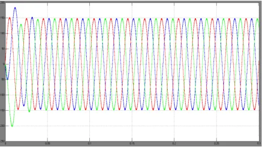
The open-loop control of the system does not achieve the control requirements for this dis-sertation and as said in the beginning of this chapter, it was only made to better understand the VSC functioning. However, the resulting VSC output current waves for an current reference of Ire fr = 150A and Ire fi = 0A can be seen in figure3.13.
As it can be seen, the current follows its reference but it has a undesired overshoot, and it takes too much time to stabilize on the desired value, which means that the control response is not fast enough. The system parameters for this simulation were:
• A DC-link voltage of Vdc= 600V ;
• The Portuguese electric grid parameters: Vg= 400V RMS , f = 50Hz;
• An impedance of: Z = 0.1 + jw1e−3in between the VSC and the grid; • A carrier wave signal frequency of: ft= 10kHz.
![Figure 2.1: Basic components and the fuel cell way of function. [1]](https://thumb-eu.123doks.com/thumbv2/123dok_br/15480644.1037822/24.892.280.569.151.374/figure-basic-components-fuel-cell-way-function.webp)

![Figure 2.15: Phase-to-neutral voltage space vectors.[5]](https://thumb-eu.123doks.com/thumbv2/123dok_br/15480644.1037822/36.892.252.602.157.433/figure-phase-to-neutral-voltage-space-vectors.webp)
![Figure 2.16: Branch voltages and space vector disposition for one switching period in sector 1.[5] [5]](https://thumb-eu.123doks.com/thumbv2/123dok_br/15480644.1037822/37.892.286.654.148.392/figure-branch-voltages-vector-disposition-switching-period-sector.webp)