Theoretical Approach to Simulate Efficient Selective Solar Absorbers With Micro or Nano
Structured Arrays
Jhong-sian Chiua, Wen-Bin Younga*
Received: November 21, 2017; Revised: February 01, 2018; Accepted: February 27, 2018
Study of the solar absorber with photonic crystal or micro structures as the heat absorbing surfaces operated at a high-temperature was conducted. Numerical calculations based on rigorous coupled-wave analysis were performed to determine the absorptance of the photonic crystal surface on the absorber.
The effect of nano geometry of the photonic crystal in tungsten on the selectivity of the absorber was investigated first, including period (L), aperture (A) and depth (d). A design algorithm for the photonic
crystal heat absorbing surface was summarized. Based on the results, a design with combined large and small square patterns was proposed to improve the absorptance, which demonstrated the ability to broaden
the absorbing band by mix-period nano patterns. Integration of an anti-reflection coating (ARC) on the photonic crystal using aluminum oxide (Al2O3) was also studied. It was shown that, under a specific
thickness of ARC, the absorptance can be further improved. As considering the effect of concentration coefficient on the energy absorption efficiency, it was found that a micro structure fabricated by laser ablation on stainless steel has a conversion rate over 85% in the case using a high concentrate coefficient.
Keywords: Selective solar absorber, photonic crystal, nano/micro structure, dish concentrating solar power.
*e-mail: [email protected].
1. Introduction
Design of a high efficiency solar absorber is important
in the concentrating solar power system. The primary requirements for the absorber are having a high heat absorptance at the solar spectrum region, while keeping low absorptance at the black body emittance region corresponding to the working temperature. According to the usage of structures and materials, there are six major designs of selective solar absorbers being reported in literature1: (a)
intrinsic absorbers, (b) semiconductor-metal tandems, (c) multilayer absorbers, (d) Cermets absorbers, (e) surface texturing, and (f) photonic crystals (PhC) based absorbers.
Intrinsic absorbers use intrinsic properties of the material to obtain desired spectrum, so its performance is limited by the material itself. Semiconductor-metal tandems use the properties of semiconductors with an appropriate bandgap to
absorb short wavelength radiation, and keep high reflectance
in the infrared region. The major drawback of it is being
not stable at the temperature higher than 750℃2. Both of
multilayer absorbers and cermets absorbers combine the metals and dielectrics as the structure to have good ability to adjust the desired absorbing spectrum. These materials have good performance at the mid-temperature range up to
the temperature about 700 ℃3-5. The fabrication of surface
texturing is accomplished by surface roughening technology. It traps the light of short wavelength in the texture of the
rough surface and reflects the light in longer wavelength6,7.
The last design is photonic crystals (PhC) installed on the heat
absorbing surface of the absorber. The absorbing spectrum
of PhC can be well controlled by varying the geometry sizes of the nano structures. The PhC can be installed on a surface
of a heat-resistant material having good thermal stability at
a high-temperature as tungsten (W) or tantalum (Ta).
In literature, there are many studies on optical properties
of photonic crystals concentrated on investigating the effects of
nano structures including period, aperture, depth and incident angle8-11 on the absorbing spectrum. The period of the nano
structure determines the lower bound wavelength of the absorbing band in a 0º incident angle. As the depth of the nano structure increases, the absorptance in the absorbing band region shows some periodic behavior. Increasing the depth or the aperture of
PhC structure can also increase the absorptance in absorbing band
region. The variation of the aperture will also alter the position
of the cut-off wavelength, which is approximately corresponding
to the upper bound wavelength of the absorbing band. In the recent years, literature showed that coating a
material as anti-reflection coating (ARC) with refractive
index between the index of air and the structure on the
absorber could reduce the effect of the incident angle. It
was shown that the emissivity spectrum of the tungsten
(W) cavity structure filled with the dielectric material with refractive index n=1.8 can reduce the effect of the incident
angle from 0º~45º12. There are also some reports8,9,13-16
showing that coating a thin film of Al2O3 or HfO2 on the
structure of W or Ta can improve the resistant to high
temperature and also the absorptance as well. In the actual
operation, the thin film coated on nano structure can also
In this study, numerical calculations based on rigorous coupled-wave analysis were used to determine the absorptance
of the photonic crystal surface in the absorber. The effect of
nano geometry of the photonic crystal on the selectivity of the
absorber was investigated, including period (L), aperture (A) and depth (d). Based on the results, a design with combined
large and small square patterns was proposed to improve the absorptance, which demonstrated the ability to broaden the absorbing band by mix-period nano patterns. Integration of an
anti-reflection coating on the photonic crystal using aluminum oxide (Al2O3) was also studied. The effect of concentration factor
on the absorption efficiency was also discussed, which leaded to
the possible application of micro structure design fabricated by laser ablation on the surface of the stainless steel solar absorber.
1.1 Selective absorber
The average solar absorptance ā and thermal emissivity ε of the absorber can be calculated from reflectance spectrum, and are defined as:
(1)
(2)
Where R(λ) is the reflectance, λ is the wavelength of light,
G(λ) is the solar spectrum of AM1.517, T is the operating
temperature, and B(λ, T) is the intensity of blackbody radiation spectrum at temperature T.
As a figure of merit, the solar photothermal conversion coefficient η*FOM, which is a ratio of the total absorbed energy
to the energy delivered, is defined as:
(3)
where C is the concentration factor. The conversion
coefficient η*FOM can be rearranged as following form:
(4)
(5)
where M(T) is the term represented the influence of thermal radiation and can be considered as the thermal radiation
factor. In equation (4), increasing the concentration factor
C can reduce the effect of thermal radiation factor M(T), and
that will increase the conversion coefficient. Thus, if M(T) is very small or C is very large, the photothermal conversion
efficiency is nearly proportional to the average absorptance ā. An ideal solar absorber should have high absorptance in the solar spectrum while having low emissivity in the thermal radiation spectrum. The ideal spectral absorptance of a selective absorber will have a cut-off wavelength defined
by the intersection of the concentrated solar radiation and black body emission spectra. It must be noticed that the intensity of the concentrated solar radiation depends on the concentration factor. As the concentration factor increases, the intensity of concentrated solar radiation increases also, resulting in a larger cut-off wavelength.
1.2 Simulation of RCWA
Rigorous coupled-wave analysis (RCWA) is a method for modeling the diffraction of electromagnetic waves on the periodic
grating array. It solves Maxwell's equation corresponding to the light scattering problem by using a Fourier expansion to represent the optical property at periodic grating region based on the Floquet's theorem. Since the solution is represented by
infinite Fourier expansion series, a truncation of the expansions
is necessary in evaluation of the solution. Selection of the number of Fourier terms becomes the main issue related to the accuracy of the solution18-23. In this study, we followed the
RCWA formulation and solution in literature21, and considered the
diffraction order up to ±24th terms for both X and Y directions. As shown in Fig. 1(a), we simulated the reflectance spectra
of periodic cavity array at normal incidence, so the incident angles θ, the azimuthal angle ϕ, and the polarization angle Ψ
are equal to 0º, and both the periods in X and Y direction are equal to L. The material used in this study for PhC was tungsten. We also studied the photonic crystal deposited with high step coverage ARC using Al2O3. The cross section view of a PhC
with ARC is shown in Fig 1(b) where d is the depth of the PhC pattern and t is the thickness of ARC. All the optical properties
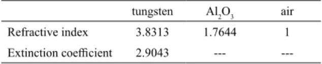
used in this study were referred from literature where those were measured at room temperature24 and listed in Table 1. ( )
( ) ( )
G d
R G d
1
0 0
a
m m
m m m
= -3
3 r " $
#
#
( ) ( , ) ( ) ( , ) TB T d
R B T d
1
0 0
f
m m
m m m
= -3 3 r " $
#
#
* * ( ) ( ) ( ) ( ) ( , )C G d
C 1 R G d 1 R B T d
FOM 0 0 0 ) h m m
m m m m m m
= - 3-
-3 3
" $ " $
#
#
#
*FOM C1*M T( )
h =ar
-( )
( ) ( ) ( , )
M T
G d
R B T d
1
0 0
m m
m m m
= -3
3
" $
#
#
Table 1. The refractive index at the wavelength of 0.667 μm
tungsten Al2O3 air
Refractive index 3.8313 1.7644 1
Extinction coefficient 2.9043 ---
---2. Result and Discussion
Two nano patterns with circular or square cavities for
PhC were included in the study. The aperture of cavity (A) is
the opening of the unit cell in the cavity pattern. In the unit
cell, a filling ratio (F) is defined as the ratio of the period (L) divided by the aperture. In the case of circular cavity,
the aperture is equal to the diameter.
2.1 Simulation model validation
For validating the simulations in this study, we simulated the periodic circular or square cavity structures which were the same geometry as in literature10,12. The nano pattern
with circular cavities had the dimensions of period L = 0.7
µm, aperture A = 0.6 µm, and depth d = 1.2 µm using the
literature. In the case of periodic pattern with square cavities, the model had periods varied from 0.4 µm to 0.6 µm, and
the aperture A = 0.8L and the depth d = A. Fig. 2 shows the
comparisons of simulation results between literature and our simulation. The simulation results for both cases with either circular or square cavities agreed quite well with literatures, which demonstrated the validity of our simulation.
Figure 1. (a) Schematic diagram of PhC model for RCWA calculations
(b) photonic crystals deposited with high step coverage ARC
Figure 2. Absorptance spectra from literature(10) and current
simulation for (a) nano circular pattern (b) flat tungsten and nano
square pattern.
2.2 Influence of geometry of the photonic crystal
In the following, we investigate the effect of period, depth, and aperture of PhC structure on reflectance spectrum. This
study used circular cavity pattern with the dimensions of
the period L = 1.6 µm and the aperture A varied from 1µm
to1.4µm. The depth was also changed from 0.05 µm to10 µm. The simulation reflectance spectrum is shown in
Fig. 3 for PhCs with the same period and different
apertures of 1.0, 1.2, and 1.4 µm. The reflectance spectra
of PhCs with different depths were also shown in the figure. For 1.0 µm aperture in Fig. 3(a), the reflectance
spectrum shows one clear trough at the position with the wavelength near the scale of the period. The reflectance at the trough of the spectrum decreases with increase
of the cavity depth and saturates beyond 3 µm (d/A=3),
indicating that, beyond this maximum depth, it will not cause any change in the reflectance spectra.
For cases with larger apertures of A = 1.2 µm or 1.4 µm, the resulting reflectance spectra are shown in
Fig. 3(b) and 3(c). In the two figures, a low reflectance
band shows up for the case when depth is larger the
ratio of d/A. The reflectance has some wavy variation at
this band, and larger depth results in lower reflectance in general. The amplitude of waviness decreases with increase of the depth also. In addition, the spectra show that the reflectance decreases with the increase of depth as well. It was concluded that, as the aperture ratio of
Figure 3. Reflectance spectrum for different depths of circular pattern in
PhC with a period L=1.6µm and aperture A= (a) 1µm (b) 1.2µm (c) 1.4µm.
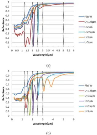
In order to show the influence of period of photonic structure on the reflectance spectrum, nano structures with different periods (1.25~5 µm) was simulated with the aperture defined in two cases as A = 1 µm and A = L-0.6 µm respectively. The
depth of the structure remains equaling to the period. Fig. 4
shows the resulting reflectance spectra of the PhCs together with the case of flat tungsten. Notice that all the spectra have a low reflectance trough at the wavelength close to period (indicated in black dash line). The result indicates that the period of the PhC structure primarily determines the region of low reflectance in the spectrum.
Figure 4. Reflectance spectrum for different periods (L) with (a)
A=1µm (b) A=L-0.6µm and depth d=A.
The reflectance spectra for the cases with fixed aperture of A = 1 µm are shown in Fig. 4(a). Under this circumstance,
the aperture ratio of aperture to period will decrease with increasing period. Following the condition discussed above, the aperture ratio must be larger than 0.7 in order to have a
low reflectance band. As sown in the figure, only the case with L = 1.25 µm fulfills this condition and shows low reflectance band in the spectrum. For larger periods, there is only a sharp decrease in reflectance at the wavelength equaling to the period. For the situation of A = L-0.6 µm, the
aperture to period ratio increases with the period. Therefore,
as the ratio is larger than 0.7 (i.e. L > 2 µm), the spectrum will have a low reflectance band as shown in Figure 4(b).
Because of the ideal cut-off wavelength changing with different operating condition, the best absorber suited for all conditions does not exist. Thus, in the following we will briefly narrate how to design a better absorber according to the result above.
At first, identify the range of wavelength which we want to absorb and the position of ideal cut-off wavelength. Then define the smallest wavelength in that range as the period of PhC structure so that the corresponding spectra will have high absorptance starting at that wavelength. With regard to solar absorbers, the better period of PhC structure is about 0.4 µm
the fabrication process, an aperture can be selected within this limit. Then, one can increase the depth until it has no
further effect on the reflectance spectrum. If the band extends beyond the cut-off wavelength, reduce the aperture and do the
study on depth again. After these procedures, one can have a
photonic crystal absorber with high efficiency.
2.3 Nano geometry of PhC
In applying PhC as the solar absorber, the patterned
structures in either circular or square cavity are commonly
found in literature. A comparison on PhC patterned with these two geometries was made to understand their effect on the solar
absorptance. Simulations were performed with the parameters
of L = 0.4 µm and d = 0.32 µm with different filling ratios. The filling ratio is defined as the ratio of the aperture to period. The calculated average absorptance of PhC with patterned structure
in square or circular cavity is shown show in Fig. 5. It is apparent
that PhC with square cavity patterned structure will have higher
absorptance as compared to the circular cavity. The absorptance
also increases with the filling ratio as discussed above. With this
result, the nano structure in square cavity pattern will be used for further discussion. The average absorptance and emittance
of type 1 PhC were listed in Table 2.
Figure 5. Average absorptance of PhC with patterned square or
circular structures in different filling ratios.
Table 2. The average absorptance and emittance of type 1 PhC
Type1 d=
0.32µm d=
0.64µm d= 1µm d=
1.5µm d= 2µm
α 0.8126 0.8273 0.8282 0.8284 0.8284
ε(1073K) 0.1015 0.1055 0.1055 0.1055 0.1055
ε(1500K) 0.1982 0.2052 0.2053 0.2053 0.2053
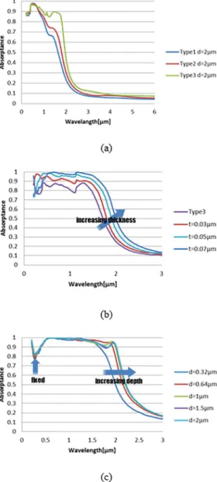
2.4 Mix-period photonic crystal
The PhC analyzed so far has the nano structure with the same period. Combination of mix-period design will be considered in this section. The PhC with the same period of L = 0.4 µm and aperture of A = 0.8L was defined
as type 1 as shown in Fig. 6. Two kinds of mix-period
patterns were designed as type 2 and 3 as well in the figure. RCWA was performed on three types of PhC. Through the comparisons of these three types, the influence of
mix-period on absorptance spectra in solar absorber was
investigated. In Fig. 7(a), the absorptance spectra of three
types show that mix-period pattern results in wider range of high absorptance band than single-period pattern. This may be caused by the superposition of the high absorptance
regions corresponding to different periods. The selected
depth of the patterned structure was 2 µm as further increase of the depth did not change the absorptance. The design of type 3 is superior to the others as it has an apparently wider high absorptance band. The average absorptance and
emittance of type 2 and 3 PhC were listed in Table 3 and 4.
Table 3. The average absorptance and emittance of type 2 PhC
Type2 d=
0.32µm d= 1µm d=
1.5µm d= 2µm d= 3µm
α 0.8374 0.8565 0.8565 0.8565 0.8565
ε(1073K) 0.1239 0.1318 0.1318 0.1318 0.1318
ε(1500K) 0.2365 0.2487 0.2487 0.2487 0.2487
Table 4. The average absorptance and emittance of type 3 PhC
Type3 d=
0.32µm d= 1µm d= 2µm d= 3µm
α 0.8074 0.8820 0.8973 0.8975
ε(1073K) 0.1289 0.1723 0.1746 0.1746
ε(1500K) 0.2442 0.3166 0.3220 0.3221
The PhC with type 3 mix-period design was used to study the effect of deposited anti-reflective coating (ARC). The material of ARC used was aluminum oxide (Al2O3), and its
optical constants were derived from the literature24. The first
case was to investigate the influence of thickness of ARC on
the absorptance spectrum. The calculated absorptance spectra
of PhC structures with different thickness of ARC from 0.03 to 0.07 µm are shown in Fig. 7(b). The absorptance of the high absorptance band increases with the ARC thickness as shown in the figure. The absorptance band only shows a shift to the right hand side with the increase of ARC thickness. Therefore, the cut-off wavelength of the absorptance spectrum increases with the ARC thickness. If one looks into the solar
irradiation spectrum, the radiation intensity rises rapidly at the wavelength of 0.3 µm, and reaches the peak at around 0.5 µm. Therefore, for application on the solar absorber,
the absorptance spectrum of PhC should be designed to
have the high absorptance band to start from 0.3 µm to the
cut-off wavelength.
The other case was to investigate the influence of the depth of type 3 structure with ARC coating. The absorptance spectra were shown in Fig. 7(c) for PhC with different structure depths from 0.32 to 2 µm and ARC coating in
0.07 µm thickness. The bandwidth of high absorptance band increases with the depth of the type 3 structure, while
the starting point of the band did not change. The cut-off
Figure 6. Top views of three nanostructure types.
Figure 7. Absorptance spectrum of (a) different PhC types (b) type
3 PhC with different ARC thickness coatings (c) type 3 PhC with different structure depths and ARC coating of 0.07µm.
To further understand the effect of the type 3 structure
depth on the thermal absorption, calculation the photothermal
conversion coefficient was done in two operating temperatures. The photothermal conversion coefficient (η*FOM) is a function
of temperature and concentration factor as shown in Eq. 3.
The ideal cut-off wavelengths for black body radiation at temperature T = 1073 K or T = 1500 k are around 2.47 µm and 1.78 µm respectively. Fig. 8 shows the η*FOM of the
type3 structure with different depths under two different temperatures. As shown in Fig. 7(c), the absorptance band
for type 3 structure was located about from 0.3 to 2.2
µm. At temperature T = 1073 K, the cut-off wavelength (2.47 µm) is larger than the band wavelength for the type 3 structures at different depths. Therefore, η*FOM increases
with the structure depth. On the other hand, for temperature
T = 1500 K, the cut-off wavelength (1.78 µm) is inside
the absorptance band at the larger structure depth. The
conversion coefficient decreases with the structure depth.
Figure 8. Figure of merit for increasing depth at temperatures
T=1073K or T=1500K.
2.5 Photothermal conversion Efficiency analysis
As discussed above about the photothermal conversion
coefficient, it depends not only on the selective absorptance
spectrum of the absorber but also on the operating
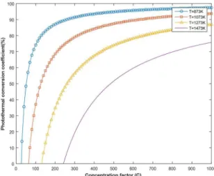
temperature. The dependence of the conversion coefficient on the temperature is through the effect of concentration
factor as shown in Eq. 4. In order to understand the
at temperatures of 873 K, 1073 K, 1273 K and 1473 K under different concentration factors as shown in Fig. 9. The conversion coefficient decreases with the increase of operating temperature under a fixed concentration factor. However, the photothermal conversion coefficient
can reach 90 % with a high concentration factor of 1000
at the temperature less than 1073 K. The result means
that, as long as the absorptance of the absorber is high
enough, it still can achieve high efficiency of photothermal
conversion without the selective absorptance spectrum.
of flat tungsten at T = 1073 K was also included. The dash
lines are the average absorptance of these three absorbers
respectively, and the efficiency can be found to increase with the concentration factor. When the operating condition is at C=1000, the η*FOM of the micro structure is about 0.87,
which has made some improvement as compared to the flat tungsten. The efficiency can be further improved by using
a design with a higher concentration factor.
Figure 9. Photothermal conversion coefficient for different
concentration factors and operating temperatures.
2.6 Micro structure
Based on the conclusion above, an absorber with high average absorptance can have photothermal conversion
up to 0.9 at the temperature below 1073 K. In order for
comparison of the performance of micro structures with
respect to PhC, an absorber was fabricated to improve
the absorptance by constructing micro scale structures on stainless steel by laser ablation using a laser engraving
machine. Parallel straight channels were cut on the surface of stainless steel. The laser ablation speed was 5 mm/sec,
the pitch was 0.04 mm, and the frequency was 20 kHz.
A spectrum analyzer was used to measure the reflectance
in the wavelength from 0.25 µm to 2.5 µm, while a Fourier Transform infrared spectroscopy was used in the wavelength from 2.5 µm to 15 µm. The derived absorptance spectra
of the absorber ablated with different laser power at 10 W, 14 W and 18 W respectively are shown in Fig. 10.
The absorptance increases with increase of laser ablation power. In the range of visible and near infrared region, the absorptance can reach 0.85~0.96 for the sample made in
power of 18 W. However, no selective band and apparent cut-off wavelength were found in the spectra.
Then the η*FOM of the micro structure fabricated by laser
power 18W was calculated to compare with the type 3 nano structure with ARC (t = 0.07 µm) in Fig 11. The spectrum
Figure 10. Absorptance spectrum of SS engraved by different
power of laser.
Figure 11. Figure of merit for three kinds of absorbers.
3. Conclusion
Photonic crystal is a good candidate as the absorbing surfaces of a solar absorber. The effect of the geometric parameters of PhC on its selective spectra was studied. The lower bound of the selective band (high absorptance) was found to near the period of the PhC structure and the upper bound was the cut-off wavelength. Larger aperture and depth of the PhC structure were preferred to have wider selective band. It was also demonstrated that the PhC with
mix period nanostructure has a wider range of selective band than the single period. Based the analysis of photothermal
conversion coefficient, absorber without selective band
operated at a high concentration factor condition can have
high photothermal conversion efficiency. Simple periodic
channels were ablated on stainless steel substrate to increase the absorptance. Based on the measured absorptance spectrum
4. References
1. Bermel P, Lee J, Joannopoulos JD, Celanovic I, Soljačić M.
Selective Solar Absorbers. Annual Review of Heat Transfer. 2012;15:231-254.
2. Moon J, Lu D, VanSanders B, Kim TK, Kong SD, Jin S, et al. High
performance multi-scaled nanostructured spectrally selective coating for concentrating solar power. Nano Energy. 2014;8:238-246.
3. Cao F, McEnaney K, Chen G, Ren Z. A review of cermet-based
spectrally selective solar absorbers. Energy & Environmental Science. 2014;7(5):1615-1627.
4. Elsarrag E, Pernau H, Heuer J, Roshan N, Alhorr Y, Bartholomé K. Spectrum splitting for efficient utilization of solar radiation:
a novel photovoltaic-thermoelectric power generation system.
Renewables: Wind, Water, and Solar. 2015;2:16.
5. Sakurai A, Tanikawa H, Yamada M. Computational design for
a wide-angle cermet-based solar selective absorber for high temperature applications. Journal of Quantitative Spectroscopy and Radiative Transfer. 2014;132:80-89.
6. Kussmaul M, Mirtich MJ, Curren A. Ion beam treatment of potential space materials at the NASA Lewis Research Center. Surface and Coatings Technology. 1992;51(1-3):299-306.
7. Lampert CM. Heat mirror coatings for energy conserving
windows. Solar Energy Materials. 1981;6(1):1-41.
8. Rinnerbauer V, Shen Y, Joannopoulos JD, Soljačić M, Schäffler F, Celanovic I. Superlattice photonic crystal as broadband
solar absorber for high temperature operation. Optics Express.
2014;22(S7):A1895-A1906.
9. Rinnerbauer V, Lausecker E, Schäffler F, Reininger P, Strasser G, Geil RD, et al. Nanoimprinted superlattice metallic photonic
crystal as ultraselective solar absorber. Optica. 2015;2(8):743-746.
10. Sai H, Yugami H, Kanamori Y, Hane K. Solar selective absorbers based on two-dimensional W surface gratings with submicron
periods for high-temperature photothermal conversion. Solar Energy Materials and Solar Cells. 2003;79(1):35-49.
11. Chen YB, Zhang ZM. Design of tungsten complex gratings
for thermophotovoltaic radiators. Optics Communications.
2007;269(2):411-417.
12. Chou J, Yeng YX, Lenert A, Rinnerbauer V, Celanovic I, Soljačić M, et al. Design of wide-angle selective absorbers/emitters with dielectric filled metallic photonic crystals for energy applications. Optics Express. 2014;22 Suppl 1:A144-154.
13. Arpin KA, Losego MD, Braun PV. Electrodeposited 3D Tungsten Photonic Crystals with Enhanced Thermal Stability. Chemistry of Materials. 2011;23(21):4783-4788.
14. Rinnerbauer V, Ndao S, Yeng YX, Senkevich JJ, Jensen KV, Joannopoulos JD, et al. Large-area fabrication of
high aspect ratio tantalum photonic crystals for
high-temperature selective emitters. Journal of Vacuum Science
& Technology B, Nanotechnology and Microelectronics:
Materials, Processing, Measurement, and Phenomena.
2013;31(1):011802.
15. Jiang D, Yang W, Tang A. A refractory selective solar absorber
for high performance thermochemical steam reforming. Applied Energy. 2016;170:286-292.
16. Rinnerbauer V, Yeng YX, Chan WR, Senkevich JJ, Joannopoulos JD, Soljacic M, et al. High-temperature stability and selective
thermal emission of polycrystalline tantalum photonic crystals. Optics Express. 2013;21(9):11482-11491.
17. National Renewable Energy Laboratory. Reference Solar Spectral Irradiance: Air Mass 1.5 Spectra. Available from:
<http://rredc.nrel.gov/solar/spectra/am1.5/>. Access in: 06/03/2018.
18. Hench JJ, Strakoš Z. The RCWA method - A case study with
open questions and perspectives of algebraic computations.
Electronic Transactions on Numerical Analysis. 2008;31:331-357.
19. Li L. Fourier modal method for crossed anisotropic gratings
with arbitrary permittivity and permeability tensors. Journal of Optics A: Pure and Applied Optics. 2003;5(4):345.
20. Li L. Use of Fourier series in the analysis of discontinuous
periodic structures. Journal of the Optical Society of America A. 1996;13(9):1870-1876.
21. Li L. New formulation of the Fourier modal method for crossed
surface-relief gratings. Journal of the Optical Society of America A. 1997;14(10):2758-2767.
22. Lalanne P, Morris GM. Highly improved convergence of the
coupled-wave method for TM polarization. Journal of the Optical Society of America A. 1996;13(4):779-784.
23. Lalanne P. Improved formulation of the coupled-wave method
for two-dimensional gratings. Journal of the Optical Society of America A. 1997;14(7):1592-1598.