PhPhPhPhPhPhPhPhPhPhPhPhPhPhPhPh
Ph
D
Electronic structure, lattice location
and stability of dopants in
wide band gap semiconductors
Marcelo Baptista Barbosa
MAP-FIS doctoral Program in Physics
Department of Physics and Astronomy Faculty of Sciences
University of Porto 2019
Supervisor
Prof. João Pedro Esteves de Araújo, FCUP
Co-Supervisor
Marcelo Baptista Barbosa
Electronic structure, lattice location and
stability of dopants in wide band gap
semiconductors
Supervisor: Prof. João Pedro Esteves de Araújo Co-Supervisor: Dr. João Guilherme Martins Correia
Thesis submitted to the Faculty of Sciences of the University of Porto in partial fulfillment of the requirements for
the degree of Doctor in Physics
Department of Physics and Astronomy Faculty of Sciences of the University of Porto
Institutions involved in this thesis:
Acknowledgements
This work is the result of the last several years of my life. Although they were full of ups and downs, of some lonely work days and frustrations but also of some really joyful mo-ments, I was never truly alone and none of this would be possible without the help and support of a lot of people around me. Therefore, I would like to thank everyone who has been by my side during all this time and made sure that I could achieve this milestone in my life! Being impossible to thank everyone by name, some special “thank you” are due.
First, I would like to thank to all the institutes and organizations that received me and allowed me to do my work, namely the Physics and Astronomy Department of the Faculty of Sciences of the University of Porto (FCUP), the Institute of Nanoscience and Nanotechnology of the University of Porto (IFIMUP-IN), the European Organization for Nuclear Research (CERN), the Center of Nuclear Physics of the University of Lisbon (CFNUL), the Nuclear and Technological Institute (recently renamed to Center of Sci-ences and Nuclear Technologies C2TN) and the “Fundação para a Ciência e a Tecnolo-gia” (FCT). To the latter, I would like to thank for my PhD scholarship with reference SFRH/BD/97591/2013.
Then, I would like to thank my supervisor Professor João Pedro Araújo for taking me under his wing very early in my career and welcoming me with arms right open into his group, always sticking by my side even during my toughest times. Thank you for all the knowledge, all the lessons and for always believing in me.
To my co-supervisor Doctor Guilherme Correia, thank you for all these years of hard work and patience when nothing wanted to work and the positive results seemed to be impossible to get. Thank you for all the emails and messages, for the long hours in Skype calls and shared screens, for teaching me how to work in the lab and for fighting with me until the good results came along.
To both my supervisors, thank you for seeing in me the potential to become a good scientist and for always pushing me in that direction. And during that process, you turned from “bosses” into friends.
Thank you to all the IFIMUP-IN family, for the amazing work environment and friend-ship you have always given me. To be more specific and in alphabetic order, thank you Ana Pires, André Pereira, Arlete Apolinário, Armandina “Dina” Lopes, Catarina Dias, Célia Sousa, Daniel silva, Diogo Costa, Gonçalo Oliveira, João Amaral, João Azevedo, João Horta, João Ventura, Luis Guerra, Mariana Proença, Sara Pinto, and Tânia
donça.
To Chico, João Horta, João (Pijri ou Chin Chen), Zé Pedro, Cocas, Ivo, Miguel (Macau) e Miguel Custódio, thank you very much for your brotherhood and for being yet another reason for me to know that I did the right choice when I decided to study Physics.
In the special case of João Horta, thank you for being my oldest companion in this Physics path, from the freshman year at the University until the end of our PhD’s, always in the same group.
To Gonçalo, thank you for all the fun night shifts at CERN. Always the best shift in business! Also, your help with all the PAC setups, mainly at CFNUL, were crucial to my work.
To André Pereira, thank you for allowing me to collaborate in some of the work you have been developing with some fellow students at the institute during the last years.
Thank you Katharina Lorenz for making me a member of your team, for letting me use some of the samples that are part of my work and for everything that I learned from you during the interpretation of my results. Moreover, thank you for the company and support that you gave me during my first presentation in an international conference, at the E-MRS.
Abel and João Nuno, thank you very much for all the help in the DFT simulations. Ricardo and Juliana, thank you for doing some of the PAC measurements that I needed for this thesis but could not do them myself.
To Doctor Lurdes Gano from C2TN, thank you very much for allowing me to use your lab for the diffusion of radioactive probes needed in some of my experiments and for all the help you gave me there.
Thank you to all my friends and family for understanding all the delayed coffees and dinners, all the absences and for always rooting for me.
To my parents and my sisters, thank you for all the love and support you always give me. Thank you for understanding the career choice that I made several years ago and for keep encouraging me, no matter what. The journey has been a lot easier having you.
And to Vanessa, you are my best friend, my girlfriend, my wife, my love and my world. Thank you for sharing your life with me and for making me try to be a better version of myself every single day. None of this would have made any sense without you. This is for you and because of you.
Resumo
A importância de materiais funcionais, tais como nano-fios e filmes finos, na ciência e tecnologia tem crescido exponencialmente nos últimos anos. Devido ao seu pequeno tamanho e crescente ratio superfície/volume, novas propriedades (previsíveis ou in-suspeitas) aparecem, com potenciais aplicações na indústria. No entanto, quanto mais pequenos os dispositivos ficam, mais as suas propriedades dependem nos factores de escala, geometria, simetria e localização de interacções de defeitos e impurezas, os quais não estão mais diluídos nos materiais constituintes[1,2]. Para além disso, é sabido que as posições atómicas e as cargas de valência influenciam as propriedades dos nano-materiais de forma severa, devido ao facto de dependerem no caráter local da densidade electrónica. No caso particular dos nano-fios, a sua integração em dis-positivos requer o controlo das propriedades eléctricas e da homogeneidade óptica, as quais não se conseguem atingir de forma sistemática[3,4]. Devido ao facto da dopagem
durante o crescimento ser principalmente governada por reacções em equilíbrio ter-modinâmico, é possível ocorrerem mudanças dramáticas na morfologia, densidade, alinhamento e homogeneidade durante esse processo (por exemplo, a concentração de dopantes é normalmente maior nas regiões próximas da superfície[4,5]). Por outro lado, a implantação iónica tem mostrado ser uma técnica de dopagem bastante ver-sátil. No entanto, tem algumas características inerentes e pouco desejadas no que toca aos defeitos de implantação, os quais precisam ser removidos, normalmente através de recozimento, de forma a ativar os dopantes. A técnica de Correlações Angulares Perturbadas (PAC) é particularmente adequada para se seguirem estes processos à escala atómica enquanto se estudam as interacções das sondas implantadas com de-feitos pontuais e impurezas/dopantes introduzidos por implantação iónica, difusão ou quando depositadas por evaporação em superfícies de filmes finos. Depois de se re-alizar o recozimento adequado, podem-se combinar as técnicas de PAC e−− γ e γ − γ para se obter uma imagem dinâmica das excitações electrónicas induzidas localmente e subsequentes fenómenos de recombinação na vizinhança das sondas.
No presente trabalho, esta metodologia foi utilizada para investigar a estrutura eletrónica, estabilidade e posição de átomos dopantes em pastilhas de pó, filmes finos e nano-fios dos semicondutores de grande hiato Ga2O3, GaN and ZnO, para os quais é fácil
crescer filmes finos e nano-fios com bom controlo nos comprimentos, diâmetros e ratio de proporcionalidade. Estes materiais têm grande potencial para aplicações em nano-e micronano-elnano-ectrónica, optonano-elnano-ectrónica nano-e nano-snano-ensornano-es[1,3–6].
Contudo, anteriormente a este trabalho não existia nenhuma ferramenta disponível para analisar dados experimentais onde o campo hiperfino na vizinhança das
das fosse dependente do tempo, tal como no caso de sondas com decaimento por captura de eletrões (ex., 111In/111Cd) ou por emissão de electrões de conversão (ex.,
181Hf/181Ta). Assim sendo, a primeira parte deste trabalho foi o desenvolvimento de
PACme, um programa em C++ que permite a simulação, análise e visualização do observável experimental de PAC para campos hiperfinos estáticos e dinâmicos (de-pendentes do tempo), considerando um conjunto de diferentes estados estocásticos possíveis e das transições entre eles. É completamente generalizado em relação ao número de diferentes frações (ambientes da sonda) e diferentes estados de cada fração, spin nuclear das sondas e estrutura cristalina (monocristal ou policristal) do material em estudo. Além disso, é o primeiro software, que tenhamos conhecimento, a integrar de forma analítica uma distribuição estática da frequência para cada estado individual em casos dinâmicos, onde a frequência que caracteriza um único estado deixa de ser um valor preciso e passa a ser representada por uma curva de distribuição normalizada centrada nesse valor. Distribuições estáticas são cruciais na análise dos espectros de PAC porque pequenos desvios no gradiente de campo elétrico e/ou no campo mag-nético à volta de sondas em posições equivalentes da rede cristalina (ex., devido a defeitos distantes das sondas) são muito frequentes e alteram o espectro de forma significativa.
As primeiras medidas de PAC foram realizadas em função da temperatura de recoz-imento após a implantação de sondas de111mCd em amostras de ZnO/CdZnO e Ga2O3.
Em ZnO, foi observada a substituição de sondas de Cd nos sítios de Zn, assim como a formação de complexos sonda-defeito. A estrutura ternária CdxZn1 – xO (x = 0.16)
apresentou boa qualidade macroscópica do cristal mas revelou algum aglomerado de defeitos locais à volta das sondas de Cd, os quais não desapareceram com o recozi-mento. Nas amostras de Ga2O3, foi observada a substituição de sondas Cd nos sítios
octaédricos do Ga, demonstrando o potencial da implantação iónica para a dopagem de nano-fios[2].
Utilizando o conhecimento adquirido nas primeiras experiências, novas medidas de PAC foram feitas após a implantação de sondas de111mCd e difusão de sondas de111In, ambas decaindo para o isótopo estável 111Cd, em amostras de Ga2O3. A localização
na rede e estado de carga dos átomos de Cd foram determinados ao comparar os resul-tados de PAC com as simulações realizadas através da teoria da densidade funcional (DFT). Uma análise abrangente sobre o impacto da introdução de átomos dopantes de Cd na rede Ga2O3 foi realizada; a densidade de estados, a estrutura de bandas e a
densidade de eletrões em redor dos átomos de Cd e dos seus primeiros vizinhos foram estudados. Foi demonstrado que o Cd induz uma banda de impurezas localizada 0,42 eV acima da banda de valência, a qual é completamente preenchida por um eletrão extra no seu estado mais estável, confirmando o seu caráter aceitador. Foi obtida uma energia de ativação de 0,54(1) eV relacionada com a mobilidade de carga eletrónica no material. Foi portanto possível confirmar que o Cd se torna num dopante aceitador no local octaédrico do Ga em Ga2O3, sendo assim um muito bom candidato para dopagem
FCUP xi Resumo
de tipo-p neste material.
Finalmente, foram realizadas medidas de PAC após a implantação de sondas de
181Hf/181Ta em amostras de GaN dopadas com Si (dopante tipo-n) e com Zn (dopante
tipo-p) com o objetivo de estudar o local na rede dos iões implantados. A combinação das técnicas de e−− γ PAC e γ − γ PAC foi utilizada para estudar a recombinação de estados eletrónicos ionizados e excitados da impureza/dopante em função da tem-peratura e do dopante. Isto demonstra o potencial uso de PAC para o estudo das propriedades elétricas de materiais onde, por exemplo, medidas do efeito Hall são difí-ceis/impossíveis de obter. Todos os resultados foram depois comparados a simulações DFT através da implementação de diferentes modelos atómicos locais, onde o gradi-ente de campo elétrico e a densidade de estados de cada configuração foram calcula-dos.
Abstract
The importance of functional nanomaterials, such as nanowires (NW) and thin films, in science and technology has been increasing exponentially over the years. Due to their small size and increasing surface-to-volume ratio, new (predictable or unsuspected) properties arise with potential applications in industry. However, the smaller the de-vices get, the more their properties depend on the scale factor, geometry, symmetry and localized interactions of defects and impurities, which are no longer diluted in the constituent materials[1,2]. Moreover, it is known that the atomic positions and charge valences severely influence the properties of nanomaterials, since they depend on the local character of the electron density. In particular for NW, their integration in de-vices requires the control of electrical properties and optical homogeneity, which is not systemically achieved[3,4]. Since doping during growth is mainly ruled by equilibrium thermodynamic reactions, a dramatical change of morphology, density, alignment and homogeneity can occur during the process (e.g., the dopant concentrations are gen-erally higher in near-surface regions[4,5]). Alternatively, ion implantation proves to be a versatile doping technique. However, it has some inherent and undesirable features regarding the effects of the implantation damage, which need to be removed, generally by thermal annealing, in order to activate the dopants. The Perturbed Angular Corre-lation (PAC) technique is particularly suitable for the follow-up of these processes at the atomic scale while studying the interactions of the implanted probe with point-like defects and impurities / dopants introduced by ion implantation, diffusion or when de-posited by evaporation (soft-landing) on surfaces and build-up interfaces of thin films. After achieving proper annealing, the combination of the e−− γ and γ − γ PAC tech-niques can be used to provide a dynamic picture of locally induced electronic excitations and subsequent recombination phenomena into the probe’s neighborhood.
In this work, this methodology was used to investigate the electronic structure, stabil-ity and lattice location of single dopant atoms in samples of powder pellets, thin films and nanowires (NW) of the wide band gap semiconductors Ga2O3, GaN and ZnO, for which
growing thin-films and NWs is well achievable, the latter with good control of lengths, diameters and “aspect ratio”. These materials have great potential for applications in nano- and microelectronics, optoelectronics and nano-sensors[1,3–6]. However, before this work there was no available tool to analyze experimental data in cases where the hyperfine field around the probes is time-dependent, such as in the case of probes which decay by electron-capture (e.g., 111In/111Cd) or by conversion electron emission (e.g.,
181Hf/181Ta). Therefore, the first part of this work was the development of PACme, a
C++ program that allows the simulation, analysis and visualization of the experimental xiii
PAC observable for static and dynamic (time-dependent) hyperfine fields considering a stochastic set of different possible states and the transitions between them. It is com-pletely generalized in terms of the number of different fractions (probe environments) and different states of each fraction, nuclear spin of the probes and crystal structure (single crystal or polycrystal) of the material under study. Moreover, it is the first soft-ware, to our knowledge, to analytically integrate a static frequency distribution for each individual state in dynamic cases, where the frequency characterizing a single state is no longer a sharp value but is instead represented by a normalized distribution curve centered at that value. Static distributions are crucial in the analysis of PAC spectra since small deviations in the electric field gradient and/or magnetic field around probes in equivalent lattice sites (e.g. due to distant defects from the probes) are very frequent and change the spectra in a very strong way. The first PAC measurements were per-formed as a function of annealing temperature after implantation of 111mCd probes in samples of ZnO/CdxZn1 – xO and Ga2O3. For ZnO, the substitution of Cd probes at Zn
sites was observed, as well as the formation of a probe-defect complex. The ternary
CdxZn1 – xO (x = 0.16) showed good macroscopic crystal quality but revealed some
clustering of local defects around the probe Cd atoms, which could not be annealed. In the Ga2O3samples, the substitution of the Cd probes in the octahedral Ga-site was
observed, demonstrating the potential of ion-implantation for the doping of nanowires[2].
Using the knowledge gained from the first experiments, new PAC measurements were performed after implantation of 111mCd probes and diffusion of 111In probes, both de-caying to stable 111Cd, in samples of Ga2O3. The location and charge state of the Cd
probe atoms were determined by comparing the PAC results to density functional theory (DFT) simulations. A comprehensive analysis regarding the impact of introducing Cd dopant atoms into the Ga2O3lattice was performed; the density of states, band structure
and the electron density around the Cd atoms and their first neighbors were studied. It was shown that Cd induces an impurity band located 0.42 eV above the valence band which is completely filled by an extra electron in its most stable state, confirming its ac-ceptor character. An activation energy of 0.54(1) eV related with the electronic charge carrier mobility in the material was obtained. It was therefore possible to confirm that Cd becomes an acceptor dopant in the octahedral Ga-site of Ga2O3, thus being a very
good candidate for p-type doping in this material. Finally, PAC measurements were performed after implantation of 181Hf/181Ta probes into Si-doped (n-type dopant) and Zn-doped (p-type dopant) samples of GaN in order to study the lattice site of the im-planted ions and the combination of the e−− γ and γ − γ PAC techniques was used to study the recombination of ionized and excited electronic states of the impurity/dopant as a function of temperature and dopant. This demonstrates the potential use of PAC for the study of electrical properties of materials where, for instance, Hall effect measure-ments are difficult / impossible to perform. All the results were later compared to DFT simulations via the implementation of different atomic local models, where the electric field gradient and density of states of each configuration was calculated.
Contents
Acknowledgements vii Resumo ix Abstract xiii Contents xvii List of Figures xxList of Tables xxi
List of Abreviations xxiii
Thesis Outline 1
1 Wide Band Gap Semiconductors 3
1.1 Ga2O3 . . . 4
1.2 GaN . . . 4
1.3 ZnO & CdxZn1 – xO . . . 5
2 Methods and Techniques 7 2.1 PAC – Perturbed Angular Correlations Spectroscopy . . . 7
2.1.1 Electric Quadrupole Interaction . . . 7
2.1.2 Magnetic Interaction . . . 11
2.1.3 Angular Correlation . . . 12
2.1.4 Perturbed Angular Correlation . . . 13
2.1.5 The Experimental Perturbation Function . . . 15
2.1.6 The Experimental Set-up . . . 17
2.1.6.1 γ− γ PAC . . . 17
2.1.6.2 e−− γ PAC . . . 18
2.2 Density Functional Theory . . . 19
2.2.1 The Born-Oppenheimer approximation . . . 20
2.2.2 The Hohenberg and Kohn theorems . . . 21
2.2.3 The Kohn-Sham method . . . 22 xv
2.2.4 The exchange-correlation functional . . . 23
2.2.5 The L/APW+lo method . . . 24
2.2.6 Calculating the Electric Field Gradient . . . 27
3 PACme: a generalized program for the simulation, analysis and visual-ization of PAC data 29 3.1 Introduction . . . 29
3.2 Theoretical Overview . . . 30
3.2.1 Hyperfine Interactions . . . 30
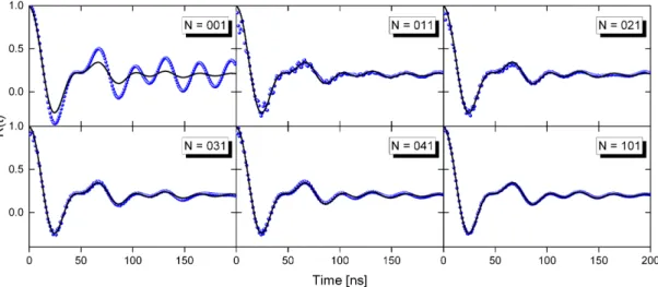
3.2.2 Perturbed Angular Correlations for Fluctuating Hyperfine Fields . . 31
3.3 Breakthrough Implementation of Static Frequency Distributions . . . 35
3.4 Test Cases and Examples . . . 37
3.4.1 Unidirectional Transition . . . 38
3.4.1.1 Simple Unidirectional Transition . . . 38
3.4.1.2 Unidirectional Transition with Static Frequency Distribu-tions . . . 40
3.4.2 XYZ model . . . 41
3.4.3 Fluctuating EFG strength in Thermal Equilibrium . . . 42
3.5 Software Overview . . . 43
3.6 Internal Algorithms . . . 44
3.6.1 χ2-function and Minuit2 . . . 45
3.6.2 Fourier transforms class . . . 46
3.7 Conclusion . . . 48
4 Cd probes location in ZnO and CdxZn1 – xO as a function of annealing temperature 51 4.1 Introduction . . . 51
4.1.1 Case studies: ZnO & CdxZn1 – xO . . . 52
4.2 Technical details . . . 52
4.3 Results and discussion . . . 53
4.3.1 ZnO . . . 53
4.3.2 Cd0.16Zn0.84O . . . 55
4.4 Conclusion . . . 59
5 Charge state and lattice location of Cd dopants in Ga2O3 61 5.1 Introduction . . . 61
5.2 Perturbed Angular Correlation experiments . . . 63
5.2.1 Experimental Details . . . 63
5.2.2 Results . . . 63
5.3 Density Functional Theory simulations . . . 66
5.3.1 Simulation details . . . 66
FCUP xvii Contents
5.4 Temperature dependence of the transition rates in PAC . . . 73
5.5 Discussion of Results and Conclusions . . . 79
6 Detailing the electronic mobility as a function of dopants in GaN 81 6.1 Introduction . . . 81
6.2 Perturbed Angular Correlation experiments . . . 82
6.2.1 Experimental Details . . . 82
6.2.2 Results . . . 83
6.3 Density Functional Theory simulations . . . 87
6.3.1 Simulation details . . . 87
6.3.2 Results . . . 87
6.4 Temperature dependence of the transition rates in e−− γ PAC . . . 93
6.5 Conclusions . . . 97
7 General Discussion and Future Perspectives 99 List of Publications and Awards 101 Bibliography 103 APPENDICES 112 A PACme – Software Documentation 113 A.1 Software Installation . . . 113
A.2 Usage Instructions . . . 114
A.2.1 Input Parameters File . . . 115
A.2.2 Output Files . . . 121
A.3 Program Structure . . . 122
A.4 External Libraries . . . 128
List of Figures
1.1 Conventional unit cell of monoclinic β-Ga2O3 . . . 4
1.2 Crystal structure of wurtzite-GaN. . . 5
1.3 Crystal structure of ZnO and CdO . . . 6
2.1 Energy splitting of a I = 5/2 intermediate nuclear level depending on η . 11 2.2 Nuclear level splitting in a B magnetic field . . . 12
2.3 A two-gamma nuclear cascade . . . 13
2.4 Experimental R(t) function and corresponding Fourier transform for spin 5/2 . . . 16
2.5 Schemes of the γ− γ PAC spectrometer . . . 17
2.6 Scheme of the e−− γ PAC spectrometer . . . 18
2.7 Flow chart for the nth iteration in the self-consistent procedure to solve the Khon-Sham equations . . . 23
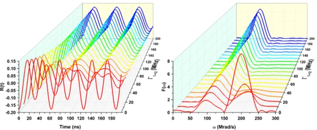
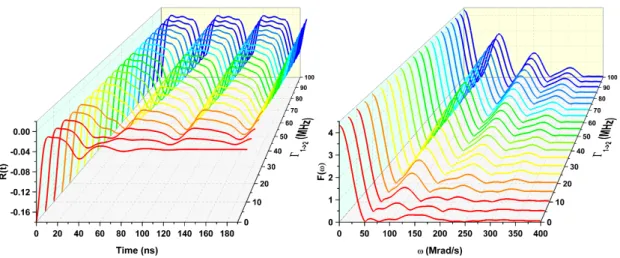
3.1 Gaussian function fitted to a sum of Lorentzian basis functions . . . 37
3.2 Unidirectional transition for spin-3/2 in a polycrystal . . . 39
3.3 Unidirectional transition for spin-5/2 in a single crystal . . . 39
3.4 Analytical integration versus a numerical integration . . . 40
3.5 Unidirectional transition from an initial state with broad static frequency distribution to a well-defined state . . . 41
3.6 XYZ model for spin-5/2 in a polycrystal . . . 41
3.7 Fluctuating EFG strength in Thermal Equilibrium . . . 42
3.8 Kaiser-Bessel window for α = 0, 2, 4, 6 and 8 . . . 49
4.1 111Cd:ZnO γ-γ PAC spectra . . . 54
4.2 111Cd:Cd0.16Zn0.84O γ-γ PAC spectra . . . 56
4.3 γ-γ PAC data of ZnO and Cd0.16Zn0.84O . . . 57
4.4 RBS/C spectra of Cd0.16Zn0.84O . . . 58
5.1 Decay scheme for 111In and 111mCd . . . 63
5.2 PAC spectra from β-Ga2O3powder pellet, nanowires and single crystal . 64 5.3 Total DOS of Ga2O3and supercells with Cd0and Cd1 – in the octahedral Ga site . . . 68
5.4 Partial DOS of Ga2O3and supercells with Cd0and Cd1 – in the octahedral Ga site . . . 69
5.5 Band structure of Ga2O3and supercell with Cd1 – in an octahedral Ga site 70
5.6 Electron density in pure Ga2O3and in Cd1 – in an octahedral Ga . . . 70
5.7 Simulated Cd sites in supercells of Ga2O3 . . . 71
5.8 Ga2O3Arrhenius plot . . . 73
5.9 (Biased) Double-Well Potential. . . 75
5.10 Illustrative curves for equations 5.1, 5.2 and 5.3 considering α = 0.3, ϵ = 0.02and ∆r= 1013. . . 77
6.1 Cascade decay and spectra of181Hf/181Ta . . . 83
6.2 γ− γ and e−− γ PAC spectra from GaN:Si . . . 84
6.3 γ− γ and e−− γ PAC spectra from GaN:Zn . . . 84
6.4 GaN Density of States . . . 88
6.5 GaN Band Structure . . . 89
6.6 GaN lattice parameters optimization . . . 89
6.7 Calculated EFG at the Ta0Ga, Ta1+Ga and Ta2+Ga sites as a function of the supercell’s lattice parameters a′ and c′ . . . 91
6.8 Density of States for GaN:Ta0Ga/Ta1+Ga/Ta2+Ga . . . 92
6.9 GaN Arrhenius plot . . . 93
6.10 GaN Band Diagram . . . 95
List of Tables
1.1 Properties of the wide band gap semiconductors β-Ga2O3, GaN and ZnO 3
4.1 111Cd:ZnO γ-γ PAC fitting parameters . . . 54
4.2 111Cd:Cd0.16Zn0.84O γ-γ PAC fitting parameters . . . 56
5.1 111In:Ga2O3γ-γ PAC fitting parameters . . . 64
5.2 Experimental and simulated EFG at the Ga and Cd sites in samples of Ga2O3 . . . 71
5.3 p, d and s-d valence contributions to the EFG for the Cd probe in Ga2O3 . 72 6.1 γ− γ PAC fitting parameters from GaN:Si and GaN:Zn . . . 85
6.2 e−− γ PAC fitting parameters from GaN:Si and GaN:Zn . . . 85
6.3 Simulated and experimental EFG at the Ta probe’s site . . . 91
A.1 Available option flags to run the program. . . 115
List of Abreviations
A
• GGA, Generalized Gradient Approximation • AFM, Atomic-Force Microscope
• C2TN, Centro de Ciências e Tecnologias Nucle-ares
• CBM, Conduction Band Minimum
• CERN, European Organization for Nuclear Re-search
• DFT, Density Functional Theory
• DLTS, Deep Level Transient Spectroscopy • DOS, Density of States
• E, Electric Field
• EFG, Electric Field Gradient
• FCUP, Faculdade Ciências da Universidade do Porto
• FWHM, Full Width at Half Maximum • HI, Hyperfine Interactions
• IFIMUP-IN, Instituto de Física dos Materiais da U-niversidade do Porto
• ISOLDE, On-line Isotope Mass Separator • J, Atom total angular momentum • L, Lattice
• LDA, Local Density Approximation • LE, Local Environment
• LED, Light-Emitting Diode • M, Magnetization
• MBE, Molecular Beam Epitaxy • MES, Mössbauer Effect Spectroscopy • MHF, Magnetic Hyperfine Field
• MOCVD, Metal-Organic Chemical Vapor Deposi-tion
• MES, Nuclear Magnetic Resonance • NW, Nanowire
• PAC, Perturbed Angular Correlations • PL, Photoluminescence Spectroscopy • RBS, Rutherford Backscattering Spectrometry • STM, Scanning-Tunneling Microscope • TCO, Transparent Conducting Oxide • VBM, Valence Band Maximum • VRH, Variable Range Hopping • WBGS, Wide Band Gap Semiconductor • XRD, X-ray Diffraction • NA, Avogadro’s number • kB, Boltzmann constant • µB, Bohr magneton • µ0H, Magnetic Induction • RT , Room Temperature • T , Temperature
• TA, Annealing Temperature • TM, Measuring Temperature • V , Volume
Thesis Outline
In an ever changing world, an invariant is emerging: our dependence on smaller, faster and more efficient electronics. Semiconductors are the foundation of modern electron-ics, but as current technology reaches its limits, where do we go next? The answer: we advance the technology we already have by using better and improved materials, such as wide band gap semiconductors (WBGS). WBGS are able to operate at very high tem-peratures, handle higher voltages and are much more efficient in terms of power losses in electricity transfer compared to current technology. They are already revolutionizing our day-to-day life by enabling the production of more efficient LEDs with wavelengths that almost cover the entire visible spectra. The applicability of WBGS depends on the ability to correctly modulate their electronic properties, which is usually done by doping. This is even more important for low-dimensional samples, like thin films and nanowires. Therefore, the ability to study the impact of dopants and the environment around them in such samples at the lowest possible scale is paramount.
Having this in mind, this thesis is the culmination of several years of research done primarily on the development of methods to study the lattice location, stability and elec-tronic properties of dopants at the nanoscale and, secondly, apply such methods to study the doping of Cd and Ta in the wide band gap semiconductors such as Ga2O3,
GaN and ZnO.
The experimental technique that was used is called Perturbed Angular Correlation (PAC) and it works by implanting radioactive isotopes in a sample which decay in a dou-ble cascade, therefore existing an angular correlation between the direction of emission of both photons (or conversion electron, depending on the isotope), which is dependent on the hyperfine fields around the probe. This enables the measurement (at the atomic scale) of the position of the probes within the crystal lattice and their charged state as a function of time and temperature, as well as the mobility of charges in the material itself. These experiments were performed at ISOLDE-CERN, the best place to get a clean beam of ‘̀any’́ chosen isotope, and at CFNUL, in Lisbon. Then, by doing Density Functional Theory (DFT) simulations, it was possible to confirm the lattice location and charged state of the dopants in the materials as well as the resulting density of states, band structure, electron density, etc.
This thesis is outlined as follows:
Chapter 1: Brief review on the main characteristics of Wide Band Gap
Semiconduc-tors, specifically on the materials under study in this work: Ga2O3, GaN and ZnO.
Chapter 2: Overview of the experimental technique used in the experiments,
Per-turbed Angular Correlation, explaining the possibility and the advantage of doing both
γ− γ and e−− γ PAC, as well as of Density Functional Theory (DFT), the method used
for the several simulations performed regarding the different materials and probes.
Chapter 3: Explanation about the development of PACme, a C++ program that
al-lows the simulation, analysis and visualization of the experimental PAC observable for static and dynamic (time-dependent) hyperfine fields. It includes several test cases and examples to showcase the potentialities of the program.
Chapter 4: Location of111mCd/111Cd probes as a function of annealing temperature in thin films of ZnO and Cd0.16Zn0.84O.
Chapter 5: Location and charge state of Cd dopants in Ga2O3 after diffusion of 111In/111Cd probes, revealing that Cd is a good candidate for p-type doping in this
ma-terial.
Chapter 6: γ− γ and e−− γ PAC measurements in Si- and Zn-doped samples of
GaN to study the location and charged states of Ta in the material as well as the impact of the different dopants in the electronic properties of GaN (alternative to Hall measure-ments in samples where electronic contacts are difficult).
Chapter 7: General discussion and the overall conclusions. An outlook is
addition-ally contained in this chapter, exploring the future prospects of the work presented.
Appendix A: Software documentation regarding PACme, including instructions to
install and use it.
Appendix B: M. B. Barbosa et al., ”Inside Back Cover: Nanostructures and thin
films of transparent conductive oxides studied by perturbed angular correlations (Phys. Status Solidi B 4/2013)”, Phys. Status Solidi B 250, No. 4 (2013).
CHAPTER 1
Wide Band Gap Semiconductors
Wide band gap semiconductors (WBGS) are semiconducting materials which have larger band gaps when compared to typical semiconductors (such as silicon), the latter hav-ing band gaps in the range of 1 eV to 1.5 eV, whereas WBGS have band gaps in the range of 2 eV to 5 eV. They are key components for the manufacturing of blue LEDs and lasers and can operate at much higher voltages, frequencies and temperatures than conventional semiconductors like silicon and gallium arsenide. Due to their promising technological applications, research regarding WBGS has been increasing at a high rate over the past few years.
In this work, three different WBGS were studied: gallium oxide (Ga2O3), gallium
nitride (GaN) and zinc oxide (ZnO). Some of their more important parameters are sum-marized in Table 1.1.
Table 1.1 – Properties of the wide band gap semiconductors β-Ga2O3, GaN and ZnO lattice structures.
Ga2O3 GaN ZnO
Crystal structure: monoclinic (β) wurtzite wurtzite
Space group: C2/m P 63mc P 63mc
Lattice param.: a[Å] 12.214[7]
3.189[8] 3.2489[9]
b[Å] 3.0371[7]
c[Å] 5.7981[7] 5.185[8] 5.2053[9]
Lattice angles: α = β 90° 90° 90°
γ 120° 103.83°[7] 120°
Band gap [eV]: 4.85[10] 3.50[11] 3.4[12]
Effective electron mass [me] : 0.28[10] 0.20[13] 0.24[12]
Electron mobility, µ [cm2/(Vs)] : 300[14] 1250[14] 200[12]
Density [g/cm3]: 5.85[10] 6.15[15] 5.606[12]
Melting point [◦C]: 1800[10] 2500[15] 1975[12]
Thermal expansion coefficient: a[10−6/K] 1.54[16]
5.59[17] 6.5[12] b[10−6/K] 3.37[16]
c[10−6/K] 3.15[16] 3.17[17] 3.0[12]
1.1
Ga
2O
3Ga2O3 belongs to the family of transparent conducting oxides and has been gaining
interest in recent years due to its potential application in power and high-voltage elec-tronic devices[10,18]. It is transparent in the ultraviolet (UV) range, thus being also very
promising for solar cells and UV optoelectronic devices[2,19,20]. Having a band gap of 4.8 eV[21], Ga2O3 is intrinsically an insulator, but its conductivity actually depends on
doping and growth conditions. N-type doping in this material is easily achieved but p-type doping has not been reliably proved yet, being, however, Cd a strong candidate[2]. It is usually reported that there are five different polymorphs of Ga2O3, namely, the
mon-oclinic (β-Ga2O3), rhombohedral (α), defective spinel (γ), cubic (δ), or orthorhombic (η)
structures[14]. Of these, the β-polymorph is the stable form under normal conditions and has been the most widely studied, including in this work. Thus from now on, Ga2O3will
refer exclusively to β-Ga2O3unless otherwise stated. The crystal structure of β-Ga2O3
is base-centered monoclinic with space group 12 (C2/m), having the Ga ions occupy-ing distorted tetrahedral (GaI) and octahedral (GaII) sites, and the O ions in a distorted
cubic packing with three inequivalent sites[7,22], with two threefold and one fourfold co-ordinated O (see Figure 1.1). It is usually described in a conventional unit cell (Fig. 1.1) with the lattice parameters a, b, c and β, the angle between the a and c axis.
Figure 1.1 – Conventional unit cell of monoclinic β-Ga2O3
1.2
GaN
GaN belongs to the group III nitrides, a group of very useful systems used in semicon-ductor devices, especially in the development of blue- and UV-LEDs[23,24]. It has a wide band-gap of 3.503(5) eV[11]and exhibits piezoelectricity, high thermal conductivity,
me-FCUP 5 1.3 ZnO & CdxZn1 – xO
chanical strength, and low electron affinity, making it an excellent material for optoelec-tronic device applications such as light-emitting diodes in the UV range, field emitters for flat displays, and high-speed transistors[25]. At ambient pressure, GaN crystallizes in a hexagonal (wurtzite) structure with the space group 186 (P 63mc) and is usually grown
on sapphire or SiC substrates by molecular beam epitaxy (MBE) or metal-organic chem-ical vapor deposition (MOCVD)[13,17]. It can also be grown in the meta-stable zincblende (cubic) structure by epitaxial growth on a GaAs or SiC substrate, but in this work only the wurtzite structure is considered.
In the wurtzite structure, it contains two Ga cations and two N anions per unit cell, with all Ga cations tetrahedrally coordinated by N ions (see Figure 1.4).
Figure 1.2 – Crystal structure of wurtzite-GaN.
The acceptor electrical doping is of utmost relevance, because the nitrides have an n-type (negative) characteristic background, and most of these applications require both a p-type (positive) and an n-type doping in order to obtain a p-n junction to produce diodes[26]. Nowadays, Mg-doped p-type GaN is a core component of many optoelec-tronic devices which we find in our homes, e.g., LEDs for solid state white lighting or blue lasers[27]. N-type doping has also been achieved by introducing Si at Ga sites[28], whilst introducing Zn at Ga sites induces a deep acceptor level that compensates unintentional donor defects[29], thus having p-type dopant character.
1.3
ZnO & Cd
xZn
1 – xO
ZnO also belongs to the family of transparent conductive oxides and has been attract-ing attention for its application to UV light-emmiters, varistors, transparent high power electronics, surface acoustic wave devices, piezoelectric transducers, gas-sensing and
as a window material for display and solar cells[12]. It is available in both bulk and single crystal forms[12]. Futhermore, the possibility of growing pseudobinary compounds, for
instance using CdO, allows band gap tuning and heterostructure growth[2]. ZnO has a band gap of 3.4 eV whilst CdO has a band gap of 2.1 eV. Therefore, the ternary CdZnO can cover a spectral range extending from the ultraviolet to the yellow wavelengths[30].
However, the binary components have different crystalline structures, namely wurtzite for ZnO (Zn cations tetrahedrally coordinated by N ions) and rock salt for CdO (Cd cations octahedrally coordinated by O ions) as can be seen in Figure 1.3. As a con-sequence, the equilibrium solubility limit of CdO in ZnO is of only about 2%. Phase separation is thus an obstacle that has to be overcome when aiming at devices emitting visible light[30]. In this way, a complete understanding on the implantation site of Cd in samples of ZnO is paramount.
(a) ZnO (b) CdO
CHAPTER 2
Methods and Techniques
2.1
PAC – Perturbed Angular Correlations Spectroscopy
Perturbed Angular Correlations spectroscopy (PAC) originated in the field of nuclear physics but has since had widespread application in solid state systems, being a pow-erful technique for the microscopic investigation of solid state local phenomena. The application of PAC in the study of materials involves the (time differential) angular corre-lation between pairs of gamma rays emitted by radioactive nuclei, which work as probes of the local electric charge distributions and magnetic fields[31]. This angular
correla-tion depends on the interaccorrela-tion between the nucleus magnetic dipole or the electric quadrupole moment and the magnetic hyperfine field or electric field gradient produced at the nucleus. The hyperfine interactions are short-ranged, therefore PAC provides in-formation on the local surroundings of particular atoms, being very sensitive to changes at their vicinity and offering unique possibilities for investigation of the structure and dynamics of the nearest neighborhood of the probes[32].
Since the general theory of Perturbed Angular Correlations is mathematically com-plex and has been well explained in several textbooks[33,34]and previous thesis[35], here only the basic physics and phenomenology of this nuclear technique are discussed.
This section starts by revisiting the electric quadrupole and magnetic interactions, which are responsible for the time differential component of the angular correlation. Then, the (perturbed) angular correlation function is motivated and the experimental perturbation function is explained. In the end, the experimental set-ups for both gamma-gamma (γ− γ) and electron-gamma (e−− γ) PAC experiments are shown.
2.1.1 Electric Quadrupole Interaction
The electrostatic energy for a nuclear charge density ρ(r) in an external electrostatic potential Φ(r) is given by[34,36]
E =
∫
ρ(r)Φ(r)d3r. (2.1)
By expanding the potential in a Taylor series around r = 0 7
Φ(r) = Φ(0) + 3 ∑ i=1 ( ∂Φ ∂xi ) 0 xi+ 1 2 ∑ i,j ( ∂2Φ ∂xi∂xj ) 0 xixj + ... (2.2)
the electrostatic energy can be written as
E = qΦ0+p· ∇Φ(0) + q 6⟨r 2⟩∇2Φ(0) +e 6 ∑ i,j ΦijQij (2.3) where Φij = ( ∂2Φ ∂xi∂xj ) 0, ∇ is the gradient, ∇
2 is the laplacian, ⟨r2⟩ is the mean
square nuclear radius and the following definitions for the total charge (q), electric dipole moment (p) and electric quadrupole moment tensor (Qij)were used:
q = ∫ ρ(r)d3r (2.4) pi = ∫ xiρ(r)d3r (2.5) Qij = 1 e ∫ ρ(r)(3xixj − r2δij)d3r (2.6) The first term in equation 2.3 (zero-order term) is the Coulomb energy of a point charge in an external potential. This term only contributes to the potential energy of the crystal lattice, being the same for every isotope of the same element and thus do not contribute to energy splitting. The second term (first-order) represents the electric dipole interaction, but due to well defined parity of the nuclear wave function, this term is zero. The third and fourth terms are both contributions from the the second-order term. The first one is the monopolar term and describes the electrostatic interaction of an ex-panded nucleus with electrons in the nuclear zone (∇2Φ(0)∝ |ψ(0)|2, where−e |ψ(0)|2
is the electronic charge density at the nucleus, only non-negligible for s electrons). It contributes to the isotope shift of nuclear levels but not to their splitting, therefore it is not observed in a Perturbed Angular Correlation experiment where only the relative energy splitting of the measuring nuclear state is observedi.
The last term is the electric quadrupole interaction energy and it is responsible for the nuclear level splitting for nuclei with non-negligible electric quadrupole moment. Since Qij is a traceless matrix, it is possible to introduce the electric field gradient ten-sor Vij − 1
3Tr(Φij), which is the traceless component of the Qij tensor. The electric
quadrupole interaction energy is then invariant by substituting Qij for Vij, so it can be written as EQ= e 6 ∑ i,j VijQij (2.7)
Because the electric field gradient is a symmetric tensor, it is always possible to find
i
FCUP 9 2.1 PAC – Perturbed Angular Correlations Spectroscopy
an eigenvectors basis where Vij is diagonal. Moreover, since Vij is a traceless matrix, it can then be completely described by only two of its components. The referential axis can be chosen such that |Vzz| ≥ |Vyy| ≥ |Vxx|. Therefore, the electric field gradient is commonly described by its largest component, Vzz, and the so called asymmetry parameter η, defined as η = Vxx−Vyy
Vzz . The asymmetry parameter only takes values
between 0 and 1, and measures the deviation of the local charge distribution from axial symmetry.
Using the asymmetry parameter and the principal component of the EFG explicitly in the electric quadrupole energy yields
EQ=
eVzz
12 [3Qzz + η(Qxx− Qyy)] (2.8)
To calculate the effect of the quadrupole interaction on a nuclear state characterized by its angular momentum ℏI, the quantum formulation has to be used. The expression 2.8 remains valid for the interaction Hamiltonian ˆHQwith the quadrupole moment tensor components, Qii, substituted by the correspondent quantum operators, ˆQii. The matrix elements of any operator in the space of states defined by|I, m⟩ must be reproduced by an analogous operator formed from the angular momentum operator ˆIi. The quadrupole operator is a rank 2, symmetric, traceless tensor and hence the operator given in terms of the Ii must also have these properties. Therefore we find that the general form for
ˆ Qij must be[35,37] ⟨I, m | ˆQij | I, m⟩ = α(I)⟨I, m | 3 2 ( ˆ IiIˆj+ ˆIjIˆi ) − δijIˆ2| I, m⟩ (2.9) where α is a yet to be determined constant. It is convenient to examine the matrix element ˆQzz between states of| I, m = I⟩
⟨I, I | ˆQzz | I, I⟩ = α(I)⟨I, I | 3 2 ( ˆ IzIˆz+ ˆIzIˆz ) − ˆI2| I, I⟩ = α(I)(3I2− I (I + 1)) (2.10) = α(I)I (2I− 1) = Q where Q is the quadrupole moment and hence
α(I) = Q
I (2I− 1). (2.11)
so the quadrupole moment operator is ˆ Qij = Q I (2I− 1) [ 3 2 ( ˆ IiIˆj + ˆIjIˆi ) − δijIˆ2 ] . (2.12)
Using equation 2.12 in equation 2.8, the quadrupole interaction Hamiltonian can be written as
ˆ HQ = eQVzz 4I(2I− 1) [ 3 ˆIz2− ˆI2+ η ( ˆ Ix2− ˆIy2 )] (2.13) and taking advantage of ladder operators - the raising operator ˆI+and the lowering
operator ˆI−, ˆ I+= ˆIx+ i ˆIy ˆ I− = ˆIx− iˆIy (2.14) the final expression is
ˆ HQ= eQVzz 4I(2I− 1) [ 3 ˆIz2− ˆI2+η 2 ( ˆ I+2 + ˆI−2 )] . (2.15)
Calculating⟨I, m| ˆHQ|I, m′⟩, the only non-zero matrix elements of ˆHQare
Hm,m=ℏωQ ( 3m2− I(I + 1)) (2.16) Hm,m±2=ℏωQ 1 2η √ (I∓ m − 1) (I ∓ m) (I ± m + 1) (I ± m + 2) (2.17) where the quadrupole frequency is defined as
ωQ=
eQVzz
4I(2I− 1)ℏ (2.18)
and gives the energy scale for the nuclear quadrupole interaction.
For the particular case of an axially symmetric interaction (η = 0), the eigenvalues of the hamiltonian are
EQ=ℏωQ [
3m2− I(I + 1)] (2.19) The transition energy between two sublevels m and m′ is given by
∆EQ =ℏωQ m2− m′2 (2.20)
m2− m′2 is always integer so all transition frequencies are multiples of ωQand the fundamental observable frequency ω0, the lowest transition frequency is:
ω0= 6ωQ, for I half-interger
ω0= 3ωQ, for I integer
Is also usual to define another quantity, the fundamental frequency:
νQ =
eQVzz
ℏ = ω0
4I(2I− 1)
2πk (2.21)
where k = 3 (for I integer) and k = 6 (for I half-integer).
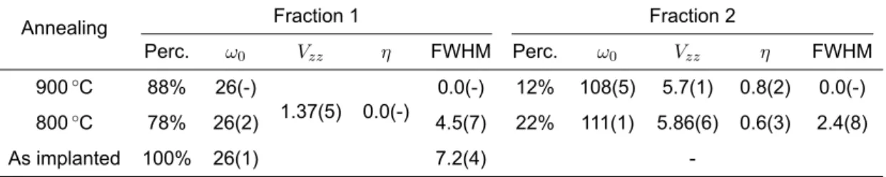
Figure 2.1 shows the electric quadrupole splitting of a nuclear level with spin I = 5/2 depending on the asymmetry parameter η. The energy splitting between the sub-levels
FCUP 11 2.1 PAC – Perturbed Angular Correlations Spectroscopy
is given by a frequency triplet ω1, ω2and ω3. In the particular case of an axially symmetric
EFG (η = 0.0), we have ω2= 2ω1 and ω3= 3ω1.
Figure 2.1 – Energy splitting of a I = 5/2 intermediate nuclear level depending on the asymmetry
pa-rameter η. (left) Dependence of the energy eigenvalues. (right) Splitting of the associated interaction frequencies.
2.1.2 Magnetic Interaction
The interaction energy between the nuclear magnetic dipole moment µ and a magnetic flux density B at the position of the nucleus is
Em =−µ · B (2.22) This interaction splits the degenerate nuclear levels into m sub-levels.
Considering a magnetic field along the z axis and the z-component of the magnetic moment, µz= gµℏNIz, the interaction energy in the state| I, m⟩ is given by
Em=⟨I, m | −µzBz | I, m⟩ = −
gµN
ℏ Bz⟨I, m | ˆIz| I, m⟩ = −gµNBzm. (2.23) The energy difference between adjacent m sub-levels is
Em(m + 1)− Em(m) =−gµNBz =ℏωL. (2.24)
where ωLis the Larmor frequency and so the splitting is the same between all con-secutive m sub-levels (see Figure 2.2).
When both magnetic and electric interactions are present, the Hamiltonian of such combined interaction, in the proper reference frame of the EFG tensor, is given by
Hcomb =
eQVzz 4I(2I− 1)
[
Figure 2.2 – Nuclear level splitting in a B magnetic field (nuclear Zeeman effect)[34].
2.1.3 Angular Correlation
The probability of emission of a photon by a radioactive nucleus depends on the an-gle between the nuclear spin axis and the direction of emission. Under ordinary cir-cumstances, the total radiation of a radioactive sample is isotropic since the nuclei are randomly oriented. However, anisotropy is verified when a nuclear state is well ori-ented. Such anisotropic γ angular distribution can be obtained if the 2I + 1 degenerate
m sub-levels cannot be equally populated, i.e., if the state from which the radiation is emitted is polarized or aligned. By definition, a state is said to be polarized when the density of states ρ(m) depends on m with ρ(m) ̸= ρ(−m), and is said to be aligned if the density of states ρ(m) of the sub-levels depends only on its absolute value, i.e,
ρ(m) = ρ(−m) ̸= ρ(m′)[33,38]. In the case of angular correlations, the oriented set of
nuclei is obtained by choosing only those nuclei whose spins happen to lie in a pre-ferred direction. Consider the case of a radioactive probe nucleus which decays in a double-cascade by emitting two consecutive γ-rays. The initial state| Ii, mi⟩ is randomly oriented and so all the different mistates are equally occupied. The observation of γ1in
a fixed direction k1(which is defined as the z axis) selects an ensemble of nuclei in the
intermediate state whose m magnetic sub-levels are no longer equally populated due to angular momentum conservation and the angular distribution of the electromagnetic radiation with respect to its angular momentum, L (see ref.[34] for more details). The
direction of emission of γ2 will then be anisotropic and so it is possible to define the
probability of measuring γ2 in a certain direction k2 at an angle θ in coincidence with
γ1, where θ is the angle between k1 and k2 (see Figure 2.3). This angular correlation is
given by[33]: W (k1,k2) = ∑ m,m′ ⟨m| ˆρ(k1) m′⟩ ⟨m′ ρ(ˆk2)|m⟩ (2.26) W (k1,k2) = W (θ) = kmax∑ k=0 Ak(γ1)Ak(γ2)Pk(cos(θ)). (2.27)
Pk(x) are the Legendre polynomialsii and reflect the spacial angular distributions
ii
A Legendre polynomial of degree n is given by Pn(x) = 2n1n! d n dxn
[
FCUP 13 2.1 PAC – Perturbed Angular Correlations Spectroscopy
of the emitted particles. Ak(γ1)and Ak(γ2)are the anisotropy terms and describe the
deviation of the coincidence probability from the isotropic case where W (θ) = 1. The latter depend on the correspondent angular momentum of the involved levels, on the type (γ, e−, β+, β−) and multipolarity of the emitted radiation and on the mixing ratios in the case of non-pure transitions. The sum is only over even k because the odd Ak(γ) vanish as a consequence of parity conservation and the fact that the polarization of the
γ photons is not measured. Also, the summation is finite due to conservation of angular momentum[31]. Moreover, it is usual to consider k
max = 4because the contributions from higher values of k are negligible. The values of the Akk = Ak(γ1)Ak(γ2)
coef-ficients for each double-cascade decay can be found in the program Nuclei[39] which uses a library developed in collaboration with the author of this thesis to calculate them (following the theoretical work on refs. 33 and 40).
Figure 2.3 – A two-gamma nuclear cascade (from ref.[31]).
Instead of measuring the directional correlation between successive γ photons, it is also possible to detect the corresponding conversion electrons and measure their correlation, thus enabling the following combinations: γ − e−, e−− γ, e−− e− . This procedure becomes feasible if at least one of the γ photons is moderately converted. In such cases, the equation 2.27 is still valid but with different anisotropy terms Ak(e−) =
bk(e−)Ak(γ)[33], where the values for particle parameter bk(e−) can be found in ta-bles[41].
2.1.4 Perturbed Angular Correlation
Note that in equation 2.27 it was used the state of the system immediately after the emission of γ1. However, this is only appropriate if the nuclei are not under the influence
of external fields. Otherwise, hyperfine interactions may cause repopulations or state transitions before the second photon is emitted. This can be represented by replacing
ˆ
ρ(k1, 0)with ˆρ(k1, t), where ˆ
and ˆΛ(t)is the time-evolution operator. Inserting 2.28 into 2.26, it can be shown that the angular correlation function becomes[33,35]
W (k1,k2, t) = ∑ k1,k2,N1,N2 Ak1(γ1)Ak2(γ2)G N1N2 k1k2 (t) YN1∗ k1 (θ1, ϕ1)Y N2 k2 (θ2, ϕ2) √ (2k1+ 1) (2k2+ 1) (2.29)
where the angles θiand γiin the spherical harmonics refer to the direction of γiwith respect to the z-axis and GN1N2
k1k2 (t), the so-called perturbation factor, is given by
GN1N2 k1k2 (t) = ∑ ma,mb (−1)2I+ma+mb√(2k 1+ 1) (2k2+ 1) ( I I k1 m′a −ma N1 ) × × ( I I k2 m′b −mb N2 ) ⟨mb | ˆΛ(t) | ma⟩⟨m′b| ˆΛ(t) | m′a⟩∗ (2.30)
ma,band m′a,bare the m quantum numbers of the intermediate state, the summation runs over|ma,b| ≤ I and m′a,b = ma,b− N1,2. Also, indices N1,2 are restricted to N1,2≤
k1,2. It should be noted that all time dependence and effects of the perturbation due to
the interaction of the nucleus with external electric or magnetic fields are contained in the perturbation factor.
The time-evolution operator ˆΛ(t)obeys to Schrödinger equation
∂
∂tΛ(t) =ˆ − i
ℏH ˆˆΛ(t) (2.31)
so, if the Hamiltonian ˆHis time-independent, the operator is given by ˆ
Λ(t) = e−ℏiHtˆ . (2.32)
In the special case of magnetic interactions or axially symmetric electric quadrupole interactions (η = 0), by choosing the z-axis in the direction of the axial field, the matrix elements of the time-evolution operator are
⟨mb| ˆΛ(t) | ma⟩ = ⟨mb | e− i
ℏHtˆ | ma⟩ = e−ℏiE(m)tδm,maδm,mb (2.33) where ma= mb = m, and a similar relation is valid for⟨m′b | ˆΛ(t) | m′a⟩. Substituing eq.(2.33) in eq.(2.30) results in the perturbation factor for static axial interactions
GN Nk1k2(t) =∑ m √ (2k1+ 1) (2k2+ 1) ( I I k1 m′ −m N ) ( I I k2 m′ −m N ) × (2.34) × exp { −i ℏ [ E(m)− E(m′)]t }
FCUP 15 2.1 PAC – Perturbed Angular Correlations Spectroscopy
It can be seen that only the energy differences between m sub-levels appear in the perturbation factor, so a measurement of this factor allows one to determine these en-ergy differences, and consequently the hyperfine interaction.
In the case of polycrystalline samples, the orientation of the hyperfine fields relative to the experimental frame of reference is not the same for all nuclei, hence the average of all possible orientations must be considered, which is done by integrating the Euler angles in the angular correlation function. The angular correlation function (eq. 2.29) then becomes
W (θ, t) =∑
k
Ak(γ1)Ak(γ2)Gkk(t)Pk(cos θ) , θ =∠(k1,k2) (2.35) where Pk are, once again, the Legendre polynomials and Gkk(t)is given by
Gkk(t) = 1 2k + 1 +k ∑ N =−k GN Nkk (t). (2.36)
2.1.5 The Experimental Perturbation Function
A PAC experimental setup consists in a set of detectors whose apparatus is usually done in such a way that each pair of detectors has an angle of 90° or 180° between them. If a γ photon is detected by a detector i with energy Eγ1, a clock is started. Then, after a certain amount of time, if a second γ photon is detected by another detector j with energy Eγ2, the clock is stopped and the time and detector pair are stored in the coincidence counting rate of the pair of detectors i, j, given by:
Nij(θ, t) = N0e−λtW (θ, t) + B (2.37)
where N0 is proportional to the number of radioactive nuclei present in the sample,
λ = 1/τ for the intermediate state half-life time τ , θ is the angle between the direction of emission of each γ photon, t = tγ2− tγ1, W (θ, t) is the angular correlation function and
B is proportional to the background random coincidence count rate, which is assumed to be time independent for simplicity.
After subtracting the background, B, an appropriate average of all the coincidence counting rate coming from the Nθ pairs of detectors with the same angle θ is made to minimize the effect of different detector efficiencies[42]:
N (θ, t) = Nθ√∏
ij
Nij(θ, t) (2.38)
To isolate the quantity providing all the relevant information (which is the angular correlation function, W (θ, t)) and eliminate the undesired exponential terms, the exper-imental perturbation function R(t) can be constructed as:
R(t) = 2 N (180
◦, t)− N(90◦, t)
N (180◦, t) + 2N (90◦, t) = 2
W (180◦, t)− W (90◦, t)
W (180◦, t) + 2W (90◦, t). (2.39)
since N0 and e−λtare the same for every N (θ, t).
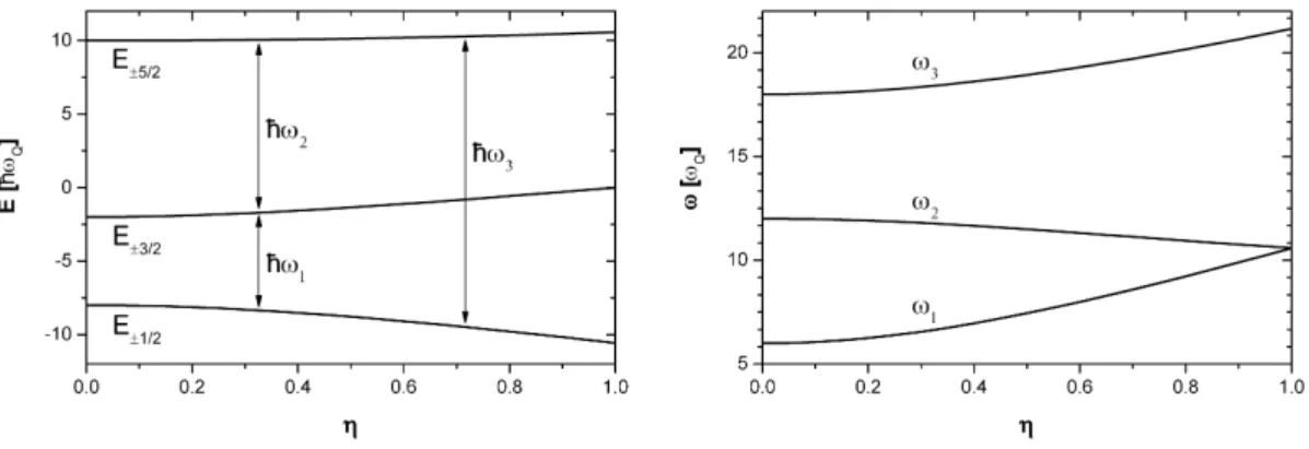
The R(t) function is the best way to get the information about the hyperfine interac-tion since it gives relevance to the perturbainterac-tion factor G(t) inside the angular correlainterac-tion function. In Fig.(2.4) an example of the R(t) function and its Fourier transform is shown for several values of η of a single EFG in a spin 5/2 intermediate nuclear level.
Figure 2.4 – Example of the experimental R(t) function and the corresponding Fourier transform for
different values of η in a spin 5/2 intermediate nuclear level, where the three characteristic frequencies (ω1, ω2, ω3)that fully characterize the EFG’s parameters Vzzand η can be seen.
EFG Distribution
The existence of lattice defects near the probes (e.g. implantation defects) can pro-duce slightly different hyperfine fields for probes that are in equivalent lattice sites. This means that instead of observing a well-defined hyperfine field, a distribution of hyper-fine fields will be measured. For low concentration of defects, such distribution in the frequency space can be approximated to a Gaussian or Lorentzian distribution and it induces an attenuation in the PAC time spectrum amplitude. For static hyperfine fields (not time-dependent), such frequency (EFG) distributions are considered in time space
FCUP 17 2.1 PAC – Perturbed Angular Correlations Spectroscopy
by multiplying each term of the R(t) perturbation function by the adequate attenuation function.
For a Gaussian frequency distribution with standard deviation σ = F W HM√
8ln 2 , the
at-tenuation function (in time space) is given by:
Dgaussian(FWHM, t) = e−
FWHM2
16ln 2t2 (2.40)
whereas for a Lorentzian distribution it is given by:
Dlorentzian(FWHM, t) = e−
FWHM 2 t
2
(2.41) where FWHM is the distribution’s Full Width at Half Maximum.
Time resolution
In order to take into account the finite time resolution (prompt) function of the spectrom-eter (which is assumed to be Gaussian-like), the coefficient of each observed frequency (ωi)is multiplied by the term P (FWHM∗, ωi), which has the form:
P (FWHM∗, ωi) = e−
FWHM∗2
16ln 2 ω2i (2.42)
2.1.6 The Experimental Set-up 2.1.6.1 γ− γ PAC
The γ-γ PAC experiments reported in this work were performed in highly efficient 4- and 6-detector PAC machines equipped with BaF2or LaBr3scintillators[43](Fig. 2.5).
Figure 2.5 – Schemes of (a) 6-detector and (b) 4-detector assembly of the γ− γ PAC spectrometer.
In the 6-detector setup, 6 γ1-γ2 coincidence time spectra from detector pairs at θ =
180° and 24 coincidence time spectra from detector pairs at θ = 90° are simultaneously recorded, in a total of 30 spectra. In the 4-detector setup, only 12 spectra are recorder: 4 from detector pairs at θ = 180° and 8 from detector pairs at θ = 90°. Using equations 2.38 and 2.39, the experimental R(t) function is given by:
R(t) = 2 6 √ 6 ∏ j Nj(180°, t)− 24 √ 24 ∏ i Ni(90°, t) 6 √ 6 ∏ j Nj(180°, t) + 224 √ 24 ∏ i Ni(90°, t)
for 6-detector set-up,
R(t) = 2 4 √ 4 ∏ j Nj(180°, t)− 8 √ 8 ∏ i Ni(90°, t) 4 √ 4 ∏ j Nj(180°, t) + 28 √ 8 ∏ i Ni(90°, t)
for 4-detector set-up.
(2.43)
The measurements can be performed in a wide range of temperatures by using a temperature-controlled furnace for the high temperatures (up to 1100◦C) and a closed-cycle helium refrigerator equipped with a proportional-integral-derivative temperature controller (PID controller) and with the sample attached to the cold finger for the low temperatures (down to 10 K). In the cryostat case, a fast load-lock sample transfer system was developed to enable the presetting of the desired temperature in the cold finger to allow low temperature measurements in short-lived isotopes.
2.1.6.2 e−− γ PAC
The e−−γ PAC spectrometer used in this work has two magnetic lenses of the Siegbahn
type[44–46]for detection of conversion electrons and two BaF2 scintillators for γ
detec-tion. Their arrangement is similar to the 4-detector PAC spectrometer set-up mentioned above, with each electron lens having a γ detector at an angle of 90° and 180° (Fig. 2.6). For measurements using a single crystalline sample, the sample surface normal usually makes 45° with both magnetic lenses.
Figure 2.6 – Scheme of the e−− γ PAC spectrometer, composed by electron (L1, L2) and gamma
(D1, D2) detectors. The sample surface normal ⃗nmakes 45° with both electron detectors (adapted
from ref.[47]).
The sample is placed inside a vacuum chamber, where the sample holder is mounted on a feed-through system that allows sample changing without breaking the vacuum in
FCUP 19 2.2 Density Functional Theory
the chamber[47,48]. Additionally, the sample holder is directly connected to the heating equipment for high temperature measurements (300 K to 1000 K) and a closed-cycle refrigerator with molecular shields allows the low temperature measurements (down to 10 K)[47].
The energy resolution of the magnetic lenses mainly depends on the lens aperture. For a specific magnetic field only electrons with the right momentum will hit the plastic scintillators and trigger a signal. Since we use isotopes with simple decay schemes, the electron lines K, L and M are well separated for wide apertures leading to∼ 1 keV energy resolution, thus improving the selection of conversion electrons from the desired transition without admixtures from other ones. Moreover, since energy selection takes place before detection, the coincidence in the detectors is significantly reduced, allowing the selection of weaker peaks in the presence of intense transitions, as well as the use of samples with stronger activity without overloading the detectors. Finally, the time resolution is also enhanced by the detection of electrons in the magnetic lenses being optimized using plastic scintillators[47].
In this set-up, 4 coincidence time spectra between a conversion electron and the γ radiation from the first and second transitions of the cascade, respectively, are recorder. There are electron-gamma detector pairs at relative angles of θ = 180° and θ = 90°, whose respective counting rates are Nj(180°, t) and Ni(90°, t) (for i, j = 1, 2). There-fore, the experimental R(t) function is given by:
R(t) = 2 √ 2 ∏ j Nj(180°, t)− √ 2 ∏ i Ni(90°, t) √ 2 ∏ j Nj(180°, t) + 2 √ 2 ∏ i Ni(90°, t) . (2.44)
2.2
Density Functional Theory
An atom consists of a positively charged nucleus, which has most of the mass in it, with negatively charged electrons in well-defined orbitals. It is the motion of the electrons and their behavior that determines the chemical properties of the atom, how it reacts with other atoms, which molecules it can form and, in final instance, the structure of the materials formed by them and their physical properties. All these properties are dependent on the motion of electrons, which is well-described by Quantum Mechanics, namely by the Schrödinger equation. Nonetheless, the idea of calculating the properties of a given material is a many-body problem not possible to completely solve analytically, since the Schrödinger equation cannot be solved exactly for more than a few electrons due to each electron not only interacting with the nucleus but also interacting with all the other electrons. Moreover, even trying to solve the equation using a computer, the more electrons are added to the system, the larger the system gets and the problem becomes exponentially difficult to compute, including for sizes much lower than the typical size of


![Figure 3.8 – Kaiser-Bessel window for α = 0, 2, 4, 6 and 8 (left) and the respective power represen- represen-tation of the Fourier transform (right) [76] .](https://thumb-eu.123doks.com/thumbv2/123dok_br/15940090.1096170/73.892.212.709.126.1000/figure-kaiser-bessel-respective-represen-represen-fourier-transform.webp)