How to simulate a semiconductor quantum dot laser: general description
(Como simular um laser de pontos quˆanticos semicondutores)George A.P. Th´
e
1Dipartimento di Elettronica, Politecnico di Torino, Corso Duca degli Abruzzi, Torino, Italy Recebido em 11/1/2008; Revisado em 11/6/2008; Aceito em 24/11/2008; Publicado em 26/6/2009
Semiconductor quantum dot laser is a recent class of laser sources which is an alternative to the conventional bulk and quantum well lasers. In the development of laser sources an important step concerns the modeling of the devices to be realized, and this requires the use of good methods able to incorporate various physical phenomena present in real devices. In this paper we show in details the implementation of a quantum dot laser simulator and apply it to simulate the switching-on behavior and other characteristics of a real quantum dot laser source. The description here presented intends to be a help for teaching or even basic-research in that particular field of optoelectronics.
Keywords: quantum dots laser, simulator, device modelling.
Laser de pontos quˆanticos semicondutores ´e uma recente classe de fontes laser que se apresenta como alterna-tiva aos lasers de po¸cos quˆanticos. Durante o desenvolvimento de fontes laser um passo importante consiste na modelagem dos dispositivos a serem realizados, e isto requer o uso de bons m´etodos, capazes de incorporar v´arios fenˆomenos f´ısicos presentes em dispositivos reais. Neste artigo mostramos em detalhes a implementa¸c˜ao de um simulador de laser de pontos quˆanticos e o aplicamos na simula¸c˜ao do comportamento deswitching-on e outras caracter´ısticas de uma fonte laser de pontos quˆanticos real. A descri¸c˜ao aqui apresentada pretende auxiliar o ensino ou mesmo a pesquisa b´asica nessa sub-´area da optoeletrˆonica.
Palavras-chave: laser de pontos quˆanticos, simulador, modelamento de dispositivo.
1. Introduction
Semiconductor lasers (SL) had their origin in 1962, when Robert N. Hall and his co-workers from General Electric demonstrated for the first time the coherent emission of light from a semiconductor diode [1], only a few years after the first demonstration of the stimulated emission in hydrogen spectra [2] in 1947, the propo-sition of the concept of light amplification by stimu-lated emission of radiation by Gordon Gould [3, 4] in 1959, the experimental realizations of a working laser (which was a solid-state flashlamp-pumped synthetic ruby crystal emitting only in pulsed regime at 694 nm) by Maiman in 1960 [5], and the realization of the first gas laser (using helium and neon) by Javan and col-leagues [6] in the same year.
The device demonstrated by Hall was made by gallium-arsenide and emitted at 850 nm (near infrared). At that time, much research started to be done aiming to show the semiconductor lasing phenomenon in differ-ent wavelengths, achievable through the use of differdiffer-ent material alloys. However, the still unpractical thresh-old current densities, Jth, of more than 50 kA/cm2was
one of the main factors that limited the room temper-ature operation of the devices. The performance of SL was improved a lot after the proposition (in 1963) of the concept of heterostructure [7, 8], which consists in the union of two semiconductor materials having differ-ent energy gaps, causing a discontinuity in the resulting energy band diagram and, thus providing carrier con-finement in the growth direction. In fact, room temper-ature operation of semiconductor lasers was possible in 1969, in pulsed mode [9], and in 1970, in CW regime [10]. Then, the next step of the progress was the reduc-tion of Jth to about 0.5 kA/cm2, an acceptable value
that put the semiconductor laser as a good technology for coherent light generation in many applications.
In 1974 a paper of Dingle and Henry changed a lot the scenario of SL technology [11]. In that work they presented the idea of exploiting quantum effects in heterostructure SL as a way to obtain wavelength tunability and achieve lower threshold lasing than in conventional (bulk) lasers. This was a seminal paper in the field of optoelectronics because it showed the ad-vantages of quantum well (QW) lasers over the conven-tional (bulk) ones, and moreover, it also gave a clear
1
E-mail: [email protected].
indication of the improved lasers that could be fab-ricated by further exploiting the reduced dimension-ality of the devices, which later would be referred to as quantum wires (2D-confinement) and quantum dots (3D-confinement). The first important advantage of QW lasers is the possibility to vary the lasing wave-length by only changing the width of the quantum well width during the growth process. Secondly, quantum well lasers can deliver more gain per injected carrier (that is, the differential gain, dg/dN is higher, thus providing higher speed) than bulk lasers; this implies that a lower threshold current density is required and, as a first consequence of the lower current injection, the internal losses,αi, are diminished in these devices.
This means higher efficiency; the second consequence is that the refractive index change is smaller in QW lasers, which means lower frequency chirp and, consequently, narrower linewidth than in bulk lasers. These advan-tages in size-quantized heterostructures come mainly from the density of states profile (DOS) for carriers near the band-edges, summarized in Fig. 1. The point is that the narrowing of the DOS distribution (as the size-quantization is increased from no-confinement up to 3D-confinement) results in confinement of carrier en-ergy distribution to narrower spectral regions. Another ingredient is that, as known from quantum mechanics [12], a high gain requires population inversion in en-ergy levels with a high density of states. In bulk lasers this takes place only after the filling of the lower lying energy levels, whereas in QW devices the peak gain is associated with energy levels at the bottom of the bands (for a complete description, seee.g.Ref. [12, chap. 10] or Ref. [13, chap. 4]). This positive effect is enhanced in QD materials, as it has ideal delta of Dirac-like den-sity of states, thus providing very high optical gain, in theory.
a) b)
c) d)
Energy - a.u.
Densityofstates-a.u.
Figura 1 - Density of statesversusenergy profile in
semiconduc-tor materials. In a) bulk material, b) quantum wells, c) quantum wires and d) quantum dots.
Indeed, in the early 80’s the increased gain of quan-tum dots was one of the motivations to researchers looking for still higher performance lasing devices. In 1986, Asada [14] theoretically demonstrated material gain in a QD up to 104 cm−1, a value much higher if
compared to the QW case. Despite of the pessimistic projections that the non-uniformity of dots size in the growth process would be crucial to the failure of QD lasers, the first experimental demonstration of lasing in self-organized dots [15] opened the way to use quan-tum dots in the active layer of SL. Low-threshold cur-rent injection was demonstrated in 1994 [16] and it was temperature-insensitive up to 150 K. In what followed, some techniques were proposed to improve the device performance, especially for what concerned the tem-perature stability of the threshold and its reduction, the room-temperature of the device and the CW power levels achievable. These techniques were the stacking of QD layers [17], the insertion of QD in a QW [18], the use of a matrix material having higher band-gap energy [19] and the seeding of QDs [20]. The evolution on the growth processes associated to the benefits car-ried on by those fundamental enhancement techniques allowed for the increased research on the use of quan-tum dot devices in a wide range of applications, from telecommunications to medicine (see, e.g., Ref. [21]). During the design of the lasers, an important and in-dispensable step concerns the modeling of the lasing properties through some computer tool (often based in a set of rate equations [22]) able to give predictions of the expected behavior of the real device, in order to check whether the specifications are matched.
In this context, in view of the increasing research interest in this field and of its relevance, in this work it is presented in details a procedure to be followed in the development of a quantum dot laser simulator. This work is organized as follows: in the next section it is made a review of a didactic and systematic procedure to easily write down the rate equations for a quantum dot laser. After that, in section 3 we describe in details the implementation of our simulator, which can be eas-ily implemented in class. To illustrate the use of the simulator, in section 4 some basic results obtained with the simulator are discussed. At last, the conclusions.
2.
Rate equations description
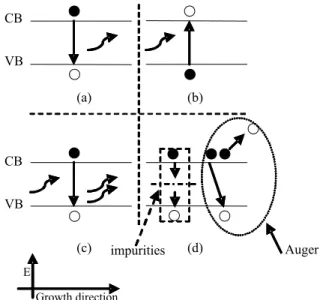
and a hole in the VB, resulting in the generation of a photon having no-correlation with other photons propa-gating in the cavity and, because of that, called incoher-ent emission. The second process represincoher-ents the pho-ton absorption by the active material, promoting the generation of an electron-hole pair, which increases the carrier density in both the CB and VB. The third tran-sition is the responsible by the optical gain inside the cavity; it represents the emission of a photon (by means of an electron-hole recombination) after the stimulus of another photon already present in the cavity. It is usu-ally said this process provides optical gain because it starts with one photon and ends with two photons. Fi-nally, the non-radiative transitions represent a class of interactions for which no-photon emission is observed. As examples of such process it can be cited recombi-nation due to semiconductor defects (and impurities), surface and interface recombination and, at last, the Auger recombination (see, e.g., Ref. [13, chaps. 1 and 4]).
Growth direction E
CB
VB
CB
VB
(a) (b)
(c) impurities (d) Auger
Figura 2 - Simplified diagram of the electronic transitions in a semiconductor material: (a) spontaneous recombination; (b) stimulated absorption; (c) stimulated emission; (d) non-radiative recombination. The dashed region in (d) represents the non-radiative recombination, such those due to semiconductor impu-rities; the circled-dotted process seen in (d) represents an Auger recombination.
In the literature of semiconductor lasers and opti-cal amplifiers those phenomena are often represented by means of time constants. Then, every transition described above can be included in a rate equations model (see, e.g., Refs. [13, 22, 23]). In this formal-ism the device to be studied is mathematically repre-sented by a set of time-differential equations for car-rier and photon densities; the time constants of every transition are included in these equations and they say the number of carriers (or photons) involved in each process in the time unit. This allows one to study, along time, the balance between electron-hole pairs genera-tion/recombination and photon generation/absorption.
These quantities will then be used to calculate the char-acteristics of interest in the design of a real device as, for instance, the output power, the laser spectrum, the net modal gain, etc. In its simplest form, the rate equations procedure consists of representing the system through a set of, at least, 2 coupled equations. One of them re-gards the carrier density, whereas the other rere-gards the photon density, the coupling being responsible by the balance between photon and carrier number inside the cavity. For the sake of simplicity, let us explain the bal-ance by assuming a constant current injection rate (this means that at each unit time a very precise amount of electron is injected into the laser active region). This pumping process increases the number of electron-hole pairs in the device (electrons in the conduction band and holes in the valence band). Besides this phenom-enon, also the photon absorption in the semiconduc-tor material increases the number of electron-hole pairs (please, refer to Fig. 2b). On the other side, the num-ber of electron-hole pairs is reduced by non-radiative recombination and photon-emitting processes, as well. By non-radiative recombination we mean a recombi-nation between one electron in the conduction band and a hole in the valence band, satisfying the selec-tion rules [13, 23], for which no photon emission is ob-served. The photon-emitting processes are those which generate photons through spontaneous recombination and stimulated emission. As it can be noticed, these processes altogether contribute to an increase or a crease in the carrier number in a time interval ∆t, de-pending whether the contribution from electron-hole generation terms is higher than that from the recombi-nation ones. The description here reviewed allows one to write the time variation of the number of carriers as
dN
dt = (Pump) + (Stim Abs)−(Stim Emis) −
(Non - radiativerec)−(Spont rec). (1)
For the photon number the idea is quite similar; from the processes cited above, one must have in mind that the stimulated emitted photons and the sponta-neous recombination processes will contribute to in-crease the photon density, because these processes are producing light inside the device, whereas the photons involved in the stimulated absorption processes cause the opposite effect, thus decreasing the fluctuation of photon number in a time interval ∆t. Besides the stim-ulated absorption, also the material optical loss will reduce the photon density; this parameter is usually expressed in units of cm−1 and expresses how many
dS
dt =−(Stim Abs) + (Stim Emis)−
(Opt loss)−(Spont rec). (2)
The Eqs. (1) and (2), after have the terms in paren-thesis replace by the real ones, constitute the set of rate equations of a bulk laser. In the case of a QD laser, the equations for carriers must be separated into dif-ferent equations accounting for carriers confined in the fundamental state (ground state, GS) and for carriers confined in the excited states (ES). Furthermore, in the literature it is often taken into account the contribution of the carriers at higher energies (for example, those in the wetting layer, WL, or in the barrier region). For the purposes of the present work, the quantum dots of the laser active region are considered to have one fun-damental confined state and the first excited state only, hereafter referred GS and ES. A typical representation of these dots, with the various processes commonly con-sidered in the modeling of quantum dot lasers is seen in the simplified diagram of Fig. 3, which shows the con-duction band profile and the various scattering events taken into account here. As a consequence of choosing the excitonic approximation to describe the interaction between electrons and holes, also in the valence band the carriers can be either in the GS or ES. This is the reason why we simply refer to one of the bands, because according to the excitonic model what happens to elec-trons in the CB happens to holes in the VB, too (see, for instance, Refs. [13, 24]).
Continuum
I e
ES
GS
GS ES ES
GS
ES
GS
t t
t
t
sp
sp
sp
tesc
hu
hu
Figura 3 - Energy diagram of a simplified quantum dot laser ac-tive region. They are shown the average times of the processes which the carriers are subject to.
From the picture we conclude that each electron of the current, I/e is directly injected into the quantum dot and become confined in the ES for a timeτGS
ES, after
which it will relax into the ground state. Besides the possibility to relax into the GS, an electron in the ES can either spontaneously recombine with a hole of the valence band (this happens every τES
sp seconds) or
un-dergo a stimulated emission process, generating a pho-ton of energy hυ equal to the energy of the incident photon. Furthermore, there is the possibility of escape
into the continuum, which happens everyτescseconds;
the electrons which get out of the dot do not contribute to the lasing. For the electrons which relax into the ground state there are practically the same processes but with different rates; the escape from the GS implies a confinement in the ES, which happens everyτES
GS
sec-onds, in average. Based on this description our model assumes the following form
dNES
dt = I
e+NGSρES
1
τES GS
−NESρGS
1
τGS ES
−
NES(1−ρES)
1
τES sp
−NES
1
τesc −
vgΓgESS
dNGS
dt =NESρGS
1
τGS ES
−NGSρES
1
τES GS
−
NGS(1−ρGS)
1
τGS sp
−vgΓgGSS
dS
dt =vgΓgGSS+vgΓgESS− S τph
+βsp
NGS
τGS sp
+
βsp
NES
τES sp
(3)
In these equationsIis the injected current,eis the unity electrical charge, ρES(GS) is the probability of
finding an empty state in the excited (ground) state, Γ is the optical confinement factor (see, e.g., Refs. [13, 23]),gES(GS)is the material gain for carriers in the
ex-cited (ground) state (Ref. [25, chap. 12]), vg is the
group velocity, βsp is the spontaneous emission factor
(gives the amount of spontaneous emission which cou-ples to the cavity optical mode),τGSsp(ES)are the
spon-taneous recombination times of carriers in the ground (excited) state, τph is the cavity photon lifetime,τESGS
is the carrier escape time from the ground state into the excited state andτGS
ES is the carrier relaxation time
from the excited state into the ground state. At last,
τescis the average time after which an electron escapes
from the dot into the continuum.
are inevitably present, consequence of the self-assembly growth process [21]. Besides, in quantum dots, due to the 3D-spatial confinement, there is a limitation in the number of carriers that can occupy a given confined state. This means that a carrier can become captured in the ES of a given dot if, and only if there is some microstate (set of quantum numbers) available at that level (Pauli Exclusion Principle). The same happens for carriers relaxing in the GS. The consequence is that the scattering events illustrated in Fig. 3 (and, thus, the time constants) are dependent on the average car-rier occupation in the confined states. On the contrary, in QW lasers carriers are free to move in a plane, and then in practice there will always be a microstate avail-able to be occupied by an “incoming” carrier, in a given confined state.
From the material point of view, this difference be-tween QW and QD lasers makes the performance of the last one higher if compared to the first one, be-cause, as mentioned before, QD lasers will require lower levels of current injection to reach threshold and to keep operating, and the threshold current will be ideally temperature-insensitive (to better understand the role of the delta of Dirac-like density of states in quantum dots, think of an ideal, isolated quantum dot with only one confined electron and one confined hole state; in this case carrier injection occurs only into these states - therefore, the population inversion is easily achiev-able - and no thermal excitation is possible - therefore, the carrier configuration in the dots is not changed by thermal effects. The result is an extremely low and temperature-insensitive threshold current). For what concerns the presence of excited states in QDs, an in-teresting consequence is that two-wavelength lasing (or more) is possible in these devices, making the emission spectrum broader and, therefore, advantageous for ap-plications like optical coherence tomography [21, 28]. Exploiting two-wavelength lasing switching in QD was demonstrated in [29] and discussed in pulse-mode in [30].
3.
Numerical solution
The set of Eqs. (3) can be solved to obtain the sta-tionary conditions by using any well-known technique based on finite difference method; in the literature it is commonly used the MATLAB solver ODE15. In this paper we show in details our implementation, which was based on a fourth-order Runge-Kutta method and showed good solvability. Let us briefly review the im-plementation of this method.
Given a differential equation of the form
dy
dx =f(x, y). (4)
one is interested in obtaining the functiony(x)
start-ing from its derivative. The Runge-Kutta method (which is an improvement of the Euler method), in its 4th-order form states that the function evaluated at a
stepi+ 1 depends on the function evaluated at the step
i and a weighted average of the function evaluated at intermediate steps betweeniandi+ 1. In the following we list this result in an appropriate way (see,e.g., Ref. [31, chap. 17])
yi+1=yi+h6(f0+ 2f1+ 2f2+f3) f0=f(x0, y0)
f1=f(x0+h2, y0+h2f0) f2=f(x0+h2, y0+h2f1) f3=f(x0+h, y0+hf2)
(5)
Now these equations have to be translated into our set of equations for carriers and photons to allow for a numerical implementation. In our problem y must be read as S, NGS and NES; his the time step dt
be-cause our equations are time-dependent (thus, xmust be translated to t). The values f0, f1, f2 and f3 are
calculated for each of the state variables and represent the differential rate equations in Eq. (3); this means the program will solve 3×4 = 12 equations per
itera-tion. The fourth-order Runge-Kutta routine developed is based on the equations below
h=dt ; x=t
f0=
fES(t
i, yi)
fGS(t i, yi)
fS(t i, yi)
,
f1=
fES(t
i+dt2, yi+dt2 ·f0) fGS(t
i+dt2, yi+dt2 ·f0) fS(t
i+dt2, yi+dt2 ·f0)
,
f2=
fES(t
i+dt2, yi+dt2 ·f1) fGS(t
i+dt2, yi+dt2 ·f1) fS(t
i+dt2, yi+dt2 ·f1)
,
f3=
fES(t
i+dt, yi+dt·f2) fGS(t
i+dt, yi+dt·f2) fS(t
i+dt, yi+dt·f2)
,
yi+1=yi+dt6 (f0+ 2f1+ 2f2+f3), yi=
NES(t
i)
NGS(t i)
S(ti)
.
(6)
As it can be seen in Eqs. (6) our data structure for the output variableyconsists on a matrix having 3 rows (1st for carriers in ES, 2nd for carriers in GS and 3rd for photons) and as many columns as the time vector is long (because our implementation is fixed-step-like). The variables assigned to f0. . . f3 are column-vectors
because they contain the solution of every rate equa-tion; these variables are supposed to be cleared after the end of each step (only after being computed in the output y). In Eq. (6) the notationfES(GS,S) stands
4.
Results
In order to motivate readers to develop this simulator for teaching and research purposes, in this section we generate a couple of results which can be used to illus-trate typical problems in optoelectronics lectures. We also point to a common research problem in the field of semiconductor lasers and present the use of the simu-lator as a tool to investigate it.
4.1. Laser switch-on
The first result concerns the laser response to an elec-trical current step injection in its active region. This is, in fact, one of the first pictures presented in a typi-cal course of optoelectronics, because it is useful to in-troduce the concept of relaxation oscillations and their origin, as well as to highlight the peak and stationary powers achievable and how they depend on the injected current, device geometry, etc. The use of the simulator provides a practical way to illustrate these dependences by only changing some parameters (e.g., those reported in the Appendix) in the program or defining them as input data. In Fig. 4 we report the switch-on for an injected current constant and equal to 24 mA. In this figure, the relaxation oscillations seen represent the in-terplay between the filling of the GS and ES energy levels with carriers and the generated photons in the cavity, thus, are related to the dynamic of carriers in-side the dots (see, e.g., Ref. [32]). Besides, readers should notice that the laser simulated in Fig. 4 reached the stationary condition at the time instantt∼3.5 ns
(hence a 5 ns-long simulation could be avoided). In a lecture should also be highlighted that even if the out-put reaches a peak near 40 mW, the stationary power is only 5.6 mW. This is an important fact concerning the application in which the device will be used; the ap-plication does determine whether these two parameters (peak power and stationary power) are acceptable.
Power(mW)
45
40
35
30
25
20
15
10
5
0
Time (ns)
0 0.5 1 1.5 2 2.5 3 3.5 4 4.5 5
Figura 4 - Laser response to a current step of 24 mA.
4.2. P-I curve
Another much popular laser feature seen very often in laser textbooks is the P-I characteristic. In the Fig. 5 is plotted the P-I of the simulation having the data pre-sented in the Appendix. The P-I curve tells one the output power of a laser when a DC current is injected into its active region, and it is drawn by taking the sta-tionary output power of different simulations, each one for a given input DC current. The P-I is indispensable in the modeling of a laser because it allows one to ob-tain the threshold current of the device to be designed, which is a very important parameter since it is strictly related to the power consumption of the laser. From the P-I one can get the threshold current by checking the current value from which the output power starts an increasing linear behavior, thereforeIth= 12 mA in
Fig. 5. Another important laser feature which can be extracted from the P-I is the slope efficiency, dP/dI, used to quantify the amount of emitted power varia-tion observed when the injected current variavaria-tion isdI, above the threshold. This parameter estimates some-how the power efficiency of the device, once higher slope efficiencies means a capability to emit more power as a response to lower current injection levels. In the simu-lation presented in Fig. 5 the slope efficiency is approx-imately 0.5 mW/mA.
Power
(mW)
4
3.5
3
2.5
2
1.5
1
0.5
0
Current (mA)
0 2 4 6 8 10 12 14 16 18 20
Figura 5 - Simulated P-I of a quantum dot laser whose parame-ters are given in Appendix. Note the threshold current equal to 12 mA.
4.3. Switch-on delay time
It was calculated as done in Ref. [33], which means we say the lasing starts (i.e., it switches-on) when the out-put power reaches 50% of the first peak value (please, refer to parameter τ in Fig. 6).
Power
(mW)
45
40
35
30
25
20
15
10
5
0
Time (ns)
0 0.5 1 1.5 2 2.5 3 3.5 4 4.5 5
Figura 6 - The switch-on time is defined as the time the laser takes to reach half the maximum power. In the figure it is repre-sented byτ.
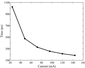
As reported in the literature (Ref. [33 and references therein]) the switch-on time is inversely proportional to the injected current and this dependence is expected to have an exponential shape; therefore the higher is the applied current over threshold, the earlier starts the las-ing. This can be seen in Fig. 7, in which the current is taken in the range [2; 4; 6; 8] ∗Ith. In the
simula-tions the current is always injected at t = 0. Besides, in Fig. 8 the expected behavior for the switch-on time
versus injected current is reported for currents ranging from 2∗Ithuntil 12∗Ith.
350
300
250
200
150
100
50
0
Power
(mW)
Time (ns)
0 0.5 1 1.5 2 2.5 3 3.5 4 4.5 5
8Ith 6Ith 4Ith 2Ith
Figura 7 - Laser time response for different values of injected current over threshold, putting in evidence that the higher is the current, the lower is the switch-on time, as known from the liter-ature (Ref. [33]).
1100
900
700
500
300
100
T
ime(ps)
Current (mA)
20 40 60 80 100 120 140 160
Figura 8 - Switch-on time versus current. This picture collects the parameterτfor different values of injected DC current. The threshold is 12 mA and this exponential behavior agrees with the literature (Ref. [33]).
Obviously, additional investigation which goes over the scope of this work can be done from this point as, for instance, the influence of relaxation time into the parameterτ, or even the influence of the geometry of the device into the switch-on time. This last, being suitable for academic purposes is reserved for a future work.
It must be emphasized that the present tool provides a simple way to study the effects of these parameters on the performance of the device and on its geometry, be-cause only a change in the input data is enough to gen-erate the output accordingly. Finally, from the imple-mentation point-of-view, the development of the sim-ulator using a fixed-step method like the fourth-order Runge-Kutta here presented is more suitable than using a variable-step one like the ODE15 of Matlab because the post-processing routines usually needed to analyze additional features of the laser output are easier to deal with in the first case.
5.
Conclusions
A quantum dot laser simulator based on the rate equa-tions formalism was presented with an academic focus. Starting from the basic concepts of electronic transi-tions, we wrote a very simplified set of 3 rate equa-tions to allow for the simulation of QD lasers. The dots were considered to have 2 confined energy levels, la-beled excited and ground state. Then, we presented in details the steps to be followed in order to solve the rate equations through the 4thorder Runge-Kutta method.
can be explored and easily illustrated with the help of such kind of simulator.
Appendix
Table containing some of the data used in the simula-tions.
Parameter Value
Device length 3 mm
Active region width 4µm Optical confinement factor 0.059 Effective refractive index 3.332 Material loss 1.5 cm−1
Dot height 6 nm
Dot radius 15.5 nm
Dot density 400µm−2 Relaxation time ES into GS 7 ps Spontaneous recombination GS 1.2 ns Spontaneous recombination ES 1.2 ns Spontaneous emission factor 10−5 Right/Left reflectivity 0.03/0.95
Acknowledgments
The Brazilian agency CNPq has supported this work (reference number 200359/2006-1).
References
[1] R.N. Hall, G.E. Fenner, J.D. Kingsley, T.J. Soltys and R.O. Carlson, Phys. Rev. Lett.9, 366 (1962).
[2] W.M. Steen, Laser Materials Processing (Springer, Berlin, 1998), 2nd
ed., 128 p.
[3] R.G. Gould, inProc. of the Ann Arbor Conference on Optical Pumping, Ann Arbor, Washington, DC (1959).
[4] S. Chu and C. Townes, inBiographical Memoirs, edited by Edward P. Lazear (National Academy of Sciences, 2003), v. 83, p. 202.
[5] T.H. Maiman, Nature187, 493 (1960).
[6] A. Javan, W.R. Bennett Jr. and D.R. Herriot, Phys. Rev. Lett.6, 106 (1961).
[7] H. Kroemer, Proc. IEEE51, 1782 (1963).
[8] Zh. I. Alferov and R.F. Kazarinov, Authors certificate 181737, U.S.S.R. (1963).
[9] H. Kressel and H. Nelson, RCA Rev.30, 106 (1969). [10] Zh. I. Alferov, V.M. Andreev, D.Z. Garbuzov, Yu. V.
Zhilyaev, E.P. Morozov, E.L. Portnoi and V.G. Trofim, Sov. Phys. Semicond.4, 1573 (1971).
[11] R. Dingle, W. Wiegmann and C.H. Henry, Phys. Rev. Lett.33, 827 (1974).
[12] P.S. Zory Jr.,Quantum Well Lasers (Academic Press, San Diego,1993).
[13] L.A. Coldren and S.W. Corzine,Diode Lasers and Pho-tonic Integrated Circuits(John Wiley & Sons, Inc, New York, 1995).
[14] M. Asada, M. Miyamoto and Y. Suematsu, IEEE J. Quantum Electron.22, 1915 (1986).
[15] N.N. Ledentsov, V.M. Ustinov, A. Yu. Egorov, A.E. Zhukov, M.V. Maximov, I.G. Tabatadze and P.S. Kop’ev, Fiz. I Tekh. Poluprovodn.28, 1484 (1994). [16] N. Kirstaedter, N.N. Ledentsov, M. Grundmann, D.
Bimberg, U. Richter, S.S. Ruvimov, P. Werner,et al., Electron. Lett.30, 1416 (1994).
[17] N.N. Ledentsov, J. B¨ohrer, D. Bimberg, S.V. Zait-sev, V.M. Ustinov, A.Yu. Egorov, A.E. Zhukov,et al., Mater. Res. Soc. Symp. Proc., edite by R.J. Shul, S.J. Pearton, F. Ren and C.-S. Wu (Pittsburgh, 1996), v. 421.
[18] Mikhail V. Maximov, Igor V. Kochnev, Yuri M. Sh-ernyakov, Sergei V. Zaitsev, Nikita Yu. Gordeev, An-drew F. Tsatsul’nikov, Alexey V. Sakharov,et al., Jpn. J. Appl. Phys. 136, 4221 (1997).
[19] N.N. Ledentsov, V.A. Shchukin, M. Grundmann, N. Kirstaedter, J. B¨ohrer, O. Schmidt, D. Bimberg,et al., Phys. Rev. B,54, 8743 (1996).
[20] M.V. Maximov, D.A. Bedarev, A.Yu. Egorov, P.S. Kop’ev, A.R. Kovsh, A.V. Lunev, Yu.G. Musikhin,et al.,Proc. ICPS24, Jerusalem, August 1998 (World Sci-entific, Singapore, 1999).
[21] M. Rossetti, Realization and Study of InAs/GaAs Quantum Dot Superluminescent Diodes Emitting at 1.3 µm, PhD Thesis, ´Ecole Polytechnique F´ed´erale de Lau-sanne, 2007.
[22] J.E. Carrol, Rate Equations in Semiconductor Elec-tronics (Cambridge University Press, Cambridge, 1985).
[23] M.A. Parker, Physics of Optoelectronics (Taylor & Francis, Boca Raton, 2005).
[24] P.Y. Yu and M. Cardona, Fundamentals of Semicon-ductors (Springer, Berlin, 1996).
[25] M. Grundmann, Nano-Optoelectronics (Springer-Verlag, Berlin, 2002).
[26] M. Gioannini, IEEE J. of Quantum Electron. 42, 331 (2006).
[27] T.B. Norris, K. Kim, J. Urayama, Z.K. Wu, J. Singh and P.K. Bhattacharya, J. Phys. D: Appl. Phys. 38, 2077 (2005).
[28] J.M. Schmitt, IEEE J. of Sel. Top. Q. Electron. 5, 4 (1999).
[29] A. Markus, M. Rossetti, V. Calligari, D. Chek-Al-Kar, J.X. Chen, A. Fiore and R. Scollo, J. of Appl. Phys. 100, 113104 (2006).
[30] G.A.P. Th´e, M. Gioannini and I. Montrosset, Proc. of 22nd
Semiconductor and Integrated Optoelectronics, Cardiff (2008).
[31] W.H. Press, S.A. Teukolsky, W.T. Vetterling and B.P Flannery, Numerical Recipes 3rd
Edition: The Art of Scientific Computing (Cambridge University Press, Cambridge, 2007).
[32] M. Grundmann, Appl. Phys. Lett.77, 10, 1428 (2000). [33] S. Ghosh, P. Bhattacharya, E. Stoner and J. Singh,