Rui Filipe Raposo Carreiras
Licenciado em Engenharia de Micro e Nanotecnologias
Nanoparticles as a charge trapping layer in
Metal-Insulator-Semiconductor structures
Dissertação para obtenção do Grau de Mestre em
Engenharia de Micro e Nanotecnologias
Orientador
: Joana Vaz Pinto
Co-orientador
: Asal Kiazadeh
Júri
Presidente: Doutor Rodrigo Ferrão Paiva Martins
Arguente: Doutora Ganga Pidyi
Vogal: Doutora Joana Vaz Pinto
Nanoparticles as a charge trapping layer in
Metal-Insulator-Semiconductor structures.
© Rui Carreiras
Faculdade de Ciências e Tecnologia
Universidade Nova de Lisboa
Nanoparticles as a charge trapping layer in
Metal-Insulator-Semiconductor structures i
ACKNOWLEDGMENTS
O final deste trabalho marca também o final de uma fase da minha vida que será relembrada no futuro com a maior das saudades. Os 5 anos de mestrado foram tempos onde dificilmente tudo o que aprendi poderá ser enumerado em tão poucas palavras.
Gostaria então de agradecer a oportunidade de frequentar este curso dada pela Universidade Nova de Lisboa, pelo Departamento de Materiais e por todos os professores que me ensinaram pelo caminho. Também não deve ser esquecido o papel desempenhado pelo CENIMAT e CEMOP, instituições que proporcionaram todas as condições para o meu trabalho ser realizado.
Um agradecimento ao presidente do departamento de ciência dos materiais Rodrigo Martins e à Diretora do CENIMAT professora Elvira Fortunato que através do seu trabalho permitiram excelentes condições para tanto a realização do curso como desta tese.
À grande ajuda dada por ambas as minhas orientadoras neste trabalho, Joana e Asal, um muito obrigado, foi uma sorte poder partilhar ideias durante estes meses.
Nanoparticles as a charge trapping layer in
Nanoparticles as a charge trapping layer in
Metal-Insulator-Semiconductor structures iii
ABSTRACT
Memories with floating gate structures are the main device architecture used in current non-volatile memories. Different films for floating gate based devices have been studied to substitute poly-crystalline silicon as the main material in floating gate structures. In current technology tunneling oxides are required to have thicknesses around 30 nm reducing device performance. Nanocrystals and nanoparticles have been emerging as a possible replacement for those films since better retention times and faster devices can be obtained. In this work the study of nanoparticles as the Charge trapping layer was executed. Study of the nanoparticles was made in a MIS structure. Hysteresis loops on C-V curves showing charge trapping was expected. Molybdenum film in the charge trapping layer was characterized as a comparison term for the nanoparticles in the CT-layer. Results of this work detail the importance of the interfacial layers, as well as defects across the oxides, on the electrical characterization of this structures. Hole trapping was achieved with nanoparticles as a charge trapping layer. Data obtained demonstrated the effect of interfacial defects in C-V curves as well as charging behavior in gold nanoparticles and Molybdenum films.
Nanoparticles as a charge trapping layer in
Nanoparticles as a charge trapping layer in
Metal-Insulator-Semiconductor structures v
RESUMO
As memórias com estrutura floating gate são a principal arquitetura utilizada atualmente em memórias não voláteis. Alternativas para o silício poly-cristalino como filme de retenção de cargas estão a ser estudadas, para eventualmente o substituírem como principal material para uma floating gate. Na tecnologia atual, os óxidos de tunelamento utilizados requerem ter 30 nm o que afeta significativamente a performance dos dispositivos. Os nanocristais e as nanopartículas estão a surgir como possíveis alternativas para filmes de retenção de cargas, permitindo óxidos de tunelamento mais finos e melhores tempos de retenção. Durante este trabalho nanopartículas como filme de retenção de cargas foi estudado. Foram utilizadas estruturas MIS para analisar a performance das nanopartículas na retenção de cargas. Os resultados esperados para este trabalho são curvas C-V com ciclos de histerese mostrando o armadilhamento de cargas. Também foram estudados filmes de molibdenio como camada de retenção de cargas como termo de comparação para os resultados obtidos com as nanopartículas. Foi identificado o fenómeno de armadilhamento de buracos nas nanopartículas. Os dados obtidos com este trabalho demonstram a importância das interfaces dos dispositivos e dos defeitos nos dielétricos na performance do dispositivo, tanto nas nanopartículas como no Molibdenio.
Palavras-chave: CT-Layers, charge trapping, nanopartículas, flash, CT-RAM , MIS , C-V , capacitance, memórias não voláteis
Nanoparticles as a charge trapping layer in
Nanoparticles as a charge trapping layer in
Metal-Insulator-Semiconductor structures vii
LIST OF ABBREVIATIONS
AuNPs – Gold nanoparticles
CEMOP – Centro de Excelência de Microelectrónica, Optolectrónica e Processos
CENIMAT | i3N – Centro de investigação de materiais/ Instituto de Nanoestruturas, Nanomodelação e Nanofabricação
RAM – Random access memory
DRAM – Dynamic Random access memory SRAM – Static Random access memory C-V – Capacitance versus voltage curve MIS – Metal insulator semiconductor structure RF – Radio frequency
FG – Floating Gate
C-t – Capacitance over time
CT-RAM – Charge trapping random access memory Flash – Flash memory
CT – Charge trapping
RTA – Rapid thermal annealing SILC – Stress induced leakage current NVM – Non-Volatile memory
TS0, 1... 6 – Different ratios between Ta2O5 and SiO2 IPA – Isopropanol
APTMS – trimethoxysilane
UVO – Ultraviolet in a Ozone atmosphere treatment JFN – Fowler-Nordheim current density
Nanoparticles as a charge trapping layer in
Nanoparticles as a charge trapping layer in
Metal-Insulator-Semiconductor structures ix
LIST OF SYMBOLS
Cs – Semiconductor capacitance C – Capacitance
CMAX – Maximum Capacitance at accumulation Ci – Insulator capacitance
C-t – Capacitance over time plot VD – Drain Voltage
VG – Gate Voltage f – frequency Vfb – Flat band voltage V – Voltage
Nanoparticles as a charge trapping layer in
Nanoparticles as a charge trapping layer in
Metal-Insulator-Semiconductor structures xi
TABLE OF CONTENTS
ACKNOWLEDGMENTS ... I
ABSTRACT ... III
RESUMO ... V
LIST OF ABBREVIATIONS ... VII
LIST OF SYMBOLS ... IX
TABLE OF CONTENTS ... XI
LIST OF FIGURES ... XIII
LIST OF TABLES ...XV
1. MOTIVATION AND OBJECTIVES ... 1
1.1. Motivation ... 1
1.2. Objectives ... 3
2. GENERAL INTRODUCTION ... 5
2.1. Non-Volatile memories and CT-RAM ... 5
2.2. Tunneling in CT-RAM... 6
2.3. Coulomb-blockade and quantum confinement effects in Retention time ... 7
2.4. Device structure and layer properties ... 8
3. MATERIALS AND METHODS ... 11
3.1. Deposition of the tunneling oxide ... 11
3.2. CT-Layer fabrication... 11
3.3. Blocking dielectric deposition ... 13
Nanoparticles as a charge trapping layer in
Metal-Insulator-Semiconductor structures xii
3.3.2. Parylene Deposition ... 13
3.4. Top and bottom contacts ... 14
3.5. Electrical and layer characterization ... 14
4. RESULTS AND DISCUSSION ... 17
4.1. Ellipsometry, Profilometry and SEM analysis ... 17
4.2. Tantalum oxide as a dielectric layer... 18
4.3. Parylene as a dielectric layer ... 21
4.4. C-V Details for MIS with CT-Layer ... 23
4.5. Molybdenum as a CT-Layer ... 24
4.6. Gold nanoparticles as a CT-Layer ... 26
4.7. Inversion on devices with Molybdenum as a CT-layer ... 28
4.8. Study of current through Silicon dioxide ... 32
5. CONCLUSIONS AND FUTURE PERSPECTIVES ... 35
5.1. Conclusions ... 35
5.2. Future perspectives... 36
6. BIBLIOGRAPHY ... 37
Nanoparticles as a charge trapping layer in
Metal-Insulator-Semiconductor structures xiii
LIST OF FIGURES
Figure 1 - Left picture is a conventional Flash memory with a floating-gate.Right picture is a charge
trapping flash memory with a nano-floating gate.[4] ... 5
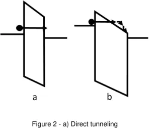
Figure 2 - a) Direct tunneling ... 7
Figure 3 - Device structure used for fabricated devices ... 9
Figure 4 - Deposition of Nanoparticles a) P-type silicon with a SiO2 layer b) Deposition of APTMS in order to functionalize the surface c) Nanoparticle deposition, they are functionalized nanoparticles and attach to APTMS ... 12
Figure 5 - Device fabrication proccess. a) P-type silicon with a SiO2 layer b) Deposition of the CT-layer c) Deposition of the blocking insulator d) Contact Deposition ... 12
Figure 6 - Parylene deposition a) P-type silicon with a SiO2 layer b) Turning SiO2 surface hydrophilic so the promotor attaches c) Promotor deposition d) Parylene deposition ... 13
Figure 7 – Shadow mask portrait ... 14
Figure 8 - C-V curve on Keithley as seen in [15] ... 15
Figure 9 – SEM image of particle distribution using Manuel et al. deposition method. ... 17
Figure 10 – C-V characteristic of a Ta2O5 MIS structure. Ratio 100/0 Tantalum/SiO2, AC Level 25 mV and 0.3 V step size ... 18
Figure 11 – Transition voltage shift on a tantalum oxide MIS for consecutive measurements with an AC Level of 100 mV and at 1 MHz. ... 19
Figure 12 – Increasing hysteresis with different sweep rates for Tantalum Oxide MIS. Measurements with 100 mV AC Level and at 10 kHz. ... 19
Figure 13 – C-V curve Parylene without CT-layer. Measurement performed at 500 kHz. Ac level 100 mV ... 21
Nanoparticles as a charge trapping layer in
Metal-Insulator-Semiconductor structures xiv
Figure 15 – C-V for Molybdenum as a CT-Layer.Measurements executed at 500 kHz, AC level of 100 mV and step 0.25 V . Small device size. Clockwise hysteresis is identified which suggests hole trapping ... 25
Figure 16 – C-V from a device with Molybdenum as a CT- Layer. Measurement at 500 kHz, 100 mV AC level and 0.2 V step size. Small device size. This sample shows a counter-clockwise hysteresis that suggests electron trapping ... 25
Figure 17 – Device with AUNP as a CT-Layer. Measurements at 100 kHZ, 100 mV AC level and 0.25 V step. Small device size. Clockwise hysteresis that suggests Hole trapping ... 26
Figure 18 - Device with AUNP as a CT-Layer. Measurements at 20 kHZ, 100 mV AC level and 0.25 V step. Small device size. Clockwise hysteresis that suggests Hole trapping ... 27
Figure 19 – Comparison between 2 samples with different CT-layers. ... 28
Figure 20 – Schematic for peripheral inversion as explained in [26]. ... 29
Figure 21 - C-V curves at different frequency of a sample with Molybdenum as a CT-Layer. Big device size.Step 0.25 V 100 mV AC level ... 30
Figure 22 – C-F curve at the inversion region of a sample with Molybdenum as a CT-layer. Big device size. ... 30
Figure 23 - C-V curves for varying sweep intervals without reaching accumulation for devices with Molybdenum as a CT-layer. Small device size. Measurements at 10 kHz, step size of 0.25 V and AC level of 100 mV... 31
Figure 24 –C-t curve for a device with Molybdenum as a CT-layer. Superimposed frequency of 10kHz with 100 mV AC level. Small device size. Development of capacitance with bias applied to the device, shows the importance of minority carriers in low frequency C-V curves. ... 32
Figure 25 – Fowler-Nordheim plot of a MIS structure with SiO2 grown by RTA as the dielectric. The I-V curves that originated this plot had a sweep interval from -8 V to 8 V. ... 33
Nanoparticles as a charge trapping layer in
Metal-Insulator-Semiconductor structures xv
LIST OF TABLES
Table 1 – Tantalum oxide C-V details for diferent thicknesses of oxide and diferent oxide to silicon dioxide ratios. ... 20
Nanoparticles as a charge trapping layer in
Nanoparticles as a charge trapping layer in
Metal-Insulator-Semiconductor structures 1
1. MOTIVATION AND OBJECTIVES
1.1. Motivation
The development of memory technologies is ever changing, the demand for faster and more reliable devices fuels new ideas and the improvement of already existing ones.
Devices that serve the purpose of storing data have a large window of characteristics that define them. All memory devices, are categorized in two types, volatile or non-volatile. Volatile memories store information in a non-permanent way, information stored needs to be connected to a power supply or to be refreshed periodically in order to retain data such as DRAM and SRAM. In Non-volatile memories, contrasting with the former devices, stored charge is semi-permanent (holds for a long time).
Non-volatile memories are available for a wide range of applications, from consumer based to industry based components, the emerging cell phone industry demands, for non-volatile memories with low power consumption and the end goal of researchers is to achieve the best non-volatile memories possible with low power consumption and high retention times.
For modern electronic circuits, flash is an indispensable component. Scaling of flash memories is not following the current CMOS device scaling and this brings problems when applying it to modern circuits. While flash memories are not scaling, power consumption of flash devices should be going down with the advances in memory research but that is not the case. Alternatives are being tested and solutions have already been provided by the scientific community to mitigate those problems.
One of the solutions for non-volatile memories that could replace flash is CT-RAM, its design allowed a decrease in thicknesses of gate oxides allowing for less power usage and faster devices. The change in charge trapping structures opened the path for layers besides standard floating gate thin films, to store the charges, with the most used being a silicon nitride layer or nanoparticle/crystals layer. This change in charge trapping layers allowed, a decrease in gate thicknesses without having a huge impact on the device performance. The study of new charge trapping layers is a good path in the improvement of non-volatile devices.[1]
Nanoparticles as a charge trapping layer in
Metal-Insulator-Semiconductor structures 2
Nanoparticles as a charge trapping layer in
Metal-Insulator-Semiconductor structures 3
1.2. Objectives
Emerging technologies in the memory industry bring the necessity for the study of different materials as constituents of new devices or better ways to use currently used materials. Electrical characterization is of the utmost importance in understanding the advantages of those materials in memory devices.
As such, the following themes will be covered:
Nanoparticles as a charge trapping layer in
Nanoparticles as a charge trapping layer in
Metal-Insulator-Semiconductor structures 5
2. GENERAL INTRODUCTION
During this chapter a brief introduction to Non-Volatile devices will be made. Following a line of thought is sought comparing current technology, flash, with CT-RAM. Finally, the mechanisms present in CT-RAMS are explained. The chapter ends with a brief explanation on the device architecture used and the role of each layer across the device.
2.1. Non-Volatile memories and CT-RAM
Demands for low power consumption and highly efficient technologies in recent electronic devices brought an ever changing memory landscape, new technologies keep being developed and less recent ones are always improving [2-3].
Even with the development of different non-volatile technologies, flash keeps being the main non-volatile technology used in current devices. In the scope of CT-RAM, flash is the most comparable device from all of the listed above and a great foundation for the understanding of CT devices.
Flash memories are achieved with a floating gate component, this area is located between the gate contact and the substrate, isolated by a blocking oxide and a tunneling oxide as seen in Figure1. Charging and discharging the floating gate allows the control of source-drain current, in order for it to be read, on write or erased state. Movement of charges into the floating gate occurs through tunneling of carriers into or out of the floating gate.
Despite obvious similarities, CT-RAM is a bit different than a flash memory, usually a standard floating gate device in flash, uses a doped polycrystalline silicon as a way to store charges. In emerging technologies different CT-layer materials are starting to be studied to replace polycrystalline silicon since its reaching its limits in terms of performance as a CT-layer in Flash devices (retention times and device power constraints). Silicon nitride and nanoparticles are the next step in non-volatile memory technologies and the development of this structures is underway.
Nanoparticles as a charge trapping layer in
Metal-Insulator-Semiconductor structures 6
In a flash memory, to achieve good write/erase times and a reasonable programming voltage, a thin tunneling layer is required (nanometric range) and this solution brings the problem of low retention times. Low retention time results from single defects in the tunneling oxide, acting as “short-circuit”. It then can cause back-tunneling from charges stored at the floating gate to source/drain or channel. Thickness of tunneling oxide should be increased to prevent this failure, resulting in a trade-off, where higher thicknesses demands higher programing voltages but with increase in the retention times. Applying a non-continuous structure (nanoparticles) would only affect charge retention for the single traps that are connected to the tunneling oxide defects, as each trap is independently dispersed across the gate dielectric. This specific conditions allow the reduction of tunneling oxide thicknesses when non-continuous charge layers are used, resulting in lower write/erase times and lower operating voltage.
Writing flash memories requires a positive gate voltage. When a positive voltage is applied, an inversion layer is created. The electric field subjected to the device, will inject inversion-layer electrons into the CT-layer, charging it. The erasing process is done by reverse biasing the gate, causing electrons to tunnel back from the charging layer into the accumulation holes from the accumulation layer [1-3][5].
2.2. Tunneling in CT-RAM
There are two prevalent tunneling mechanisms, Fowler-Nordheim and direct tunneling. The dependence of the current density with the applied bias in a MIS structure, helps identifying which type of tunneling the device is undergoing. When doing a voltage versus current density plot at different temperatures, a highly temperature dependent current density is expected to occur if Fowler-Nordheim tunneling is to be expected [6].
Nanoparticles as a charge trapping layer in
Metal-Insulator-Semiconductor structures 7
For oxide thicknesses of 4 nm or less direct tunneling is predominant, at this oxide thicknesses low electric fields are enough to tunnel carriers through the oxide without them travelling across the conduction band, when increasing oxide thicknesses Fowler-Nordheim tunneling starts to occur. The increase in thickness of the oxide allows electrons to tunnel into the conduction band of the insulator. High electric fields increase the bending of the oxide conduction band and permits electrons to tunnel through the oxide to it, and following hop to the charging layer, as can be seen in Figure 2.
Trap assisted tunneling is, as well, an issue in silicon oxide devices. Specifically, CT-RAM are not so affected by traps but when analyzing simple MIS SiO2 devices, trap assisted tunneling can occur at low electric field, its presence can mask values of direct tunneling current. In the specific case of this work, traps in the dielectric are minimized by the growth of oxide through RTA [24], but the creation of traps states when the device is under stress is still a problem. Stress induced leakage current(SILC) is the name of the current that originates from stress induced defects in the dielectric. When insulators are exposed through an electric field, trap states are created via stress. Those trap states create paths where charge carriers can tunnel to and increase trap assisted tunneling [8].
2.3. Coulomb-blockade and quantum confinement effects in Retention time
In an ideal world charges would stay in the charge trapping layer for an infinite amount of time, but that is not the case, Coulomb-blockade effects and quantum confinement do not allow to have perfect Non-volatile behavior and so they are the main reason for retention time and tunneling current problems.
Nanoparticles as a charge trapping layer in
Metal-Insulator-Semiconductor structures 8
Coulomb blockade is connected to the raise in potential energy across the charging layer. When an electron is stored in a trap, the electrostatic energy of the traps starts to increase, in consequence electrons that might tunnel to that trap have to have a higher energy to do so, as it is impossible to keep tunneling charges to already charged trapped states, current density across the oxide starts to decrease. Main factors to increase potential energy from the charging layer are related to the number of charges able to be stored by it, so logically size of traps and number of traps are the key points to tune this effect on this kind of devices. One of the upsides of this effect is being primary felt at low programming voltages, meaning that devices with this behavior have less susceptibility to low electric fields. When fast programming speed and large tunneling current is desired coulomb blockade has to be reduced, increasing the size of the defects and the increase of trapping sites allows more electrons to tunnel trough and increase the potential electrostatic energy. Despite having a high impact in current density during tunneling, coulomb blockade is a limitation to retention time. Specifically, a trade-off between retention time and programming speeds needs to be taken into account since to get high retention time potential electrostatics energy cannot be really high, because if that is the fact probability of charges back-tunneling from the charging layer to the channel or source/drain is really high.
For defects on the nanometer range, quantum confinement starts gaining significant weight on charges trapped, the upward shift on the nanocrystal conduction band reduces the conduction band offset between the nanocrystal and the surrounding oxide, at this conditions probabilities of charges tunneling back are increased, reducing retention performances of devices [1].
2.4. Device structure and layer properties
Nanoparticles as a charge trapping layer in
Metal-Insulator-Semiconductor structures 9
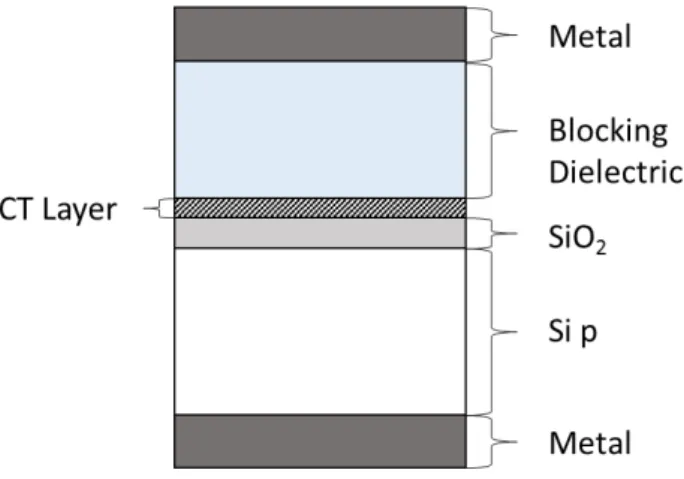
Figure 3 - Device structure used for fabricated devices
When fabricating tunneling oxides, interface properties, defects in the oxide and barrier heights have to be taken into account. In the Silicon dioxide case, having great interface properties with silicon wafers is an advantage when used as tunneling oxide, the massive study in its properties and fabrication is important for its selection as a tunneling oxide for this work. To achieve low defects, a fast process of oxidation is necessary, this requirement is consequence of the high impurity distribution that usually occurs when doing high temperature oxidation for long times [10]. Despite having good properties for a tunneling layer, SiO2 compared to other dielectrics like HfO2, lacks retention characteristics, its lower barrier allows more charges to tunnel back from the charging layer and lower dielectric constant asks for a higher electric field to induce tunneling [2-3].
For the purpose of this work gold nanoparticles were used as a CT-Layer instead of nanocrystals and as a comparison term, metallic films were also studied in order to distinguish the usage of continuous or non-continuous films for charge trapping.
Metallic nanoparticles have its benefits compared with silicon structures as they bring higher electron affinity, which allows the engineering of an asymmetric barrier between the Si channel and the storage nodes, this asymmetry allows to increase retention times without damaging write/erase speeds, metallic nanoparticles also bring less Influence from trap states at the interface since the high density of states created by the particles is around the Fermi level, meaning that charges get stored in the nanoparticles. Metallic layers share some of the properties of nanoparticles, being electron affinity and high work function the main reason for being applied in memories [5].
Nanoparticles as a charge trapping layer in
Metal-Insulator-Semiconductor structures 10
regarded as the best kind of dielectrics to use as blocking dielectric. Some materials used as blocking dielectrics have a large conduction band offset, paired with being high-k materials, it decreases immensely the probability of any back tunneling and makes them excellent blocking oxides [11].
Tantalum oxide was proposed to be used as a blocking dielectric and also as multicomponent Ta-Si-O dielectric. As the objective of this work is to see the role of the charge trapping layers and their ability to store charges, any kind of charging behavior in the blocking oxide discards it as a good solution for this devices. Tantalum oxide showed some charging behavior during testing and was ruled out as a blocking oxide.
Nanoparticles as a charge trapping layer in
Metal-Insulator-Semiconductor structures 11
3. MATERIALS AND METHODS
The description of the steps required to fabricate the devices tested in this work and the equipment for electrical and thin film characterization is detailed in this chapter.
Fabrication of CT-RAM devices required several steps in a clean room, and it is advised that every step should be reproduced in the same conditions, impurities or defects should be minimized.
Two different CT-RAM MIS structures were fabricated, one using a metal thin layer in between two dielectric layers, and another one using a monolayer of gold nanoparticles (AuNPs) in between the insulating films.
Devices were fabricated in a p-type silicon wafer, with <1 0 0> crystal orientation. The wafer has a resistivity of 1 to 2 Ωcm-1 and is doped with Boron.
3.1. Deposition of the tunneling oxide
The first step in the fabrication process is the removal of the native oxide, using a HF solution (1:100 in H2O). This process is executed by bathing the wafer in the HF solution from 2 to 5 minutes until it gets hydrophobic. When hydrophobic, it needs to be rinsed with deionized water and dried off. Upon native oxide removal, a thin thermal SiO2 layer is produced by a rapid thermal annealing (RTA) process in a O2 atmosphere.
Producing the tunneling oxide through RTA required an annealing temperature of 950º, during 6 min. Annealing was done at 100 mBar in a O2 atmosphere, as reported in [12]. Temperature rising rate was 50 º/s. At this conditions, minimal defects in the oxide are expected and thicknesses of around 8 nanometers were achieved [10].
3.2. CT-Layer fabrication
Method A – AUNPs as the CT-Layer
The method for processing the dispersed nanoparticle layer is based on reports from Mendes et. Al [12-13]. The gold nanoparticles used for this work were synthetized by BBI solutions, with an average size of 30 nm. The surface of the wafer is modified by APTMS from Sigma-Aldrich.
Nanoparticles as a charge trapping layer in
Metal-Insulator-Semiconductor structures 12
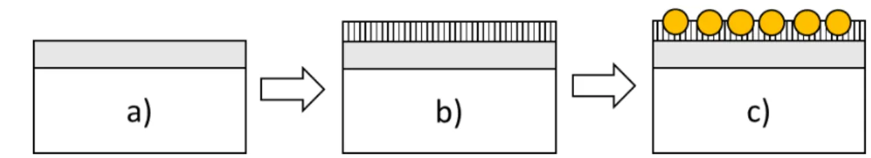
Surface modification is required in order to have a hydrophilic surface so that the APTMS attaches to the surface and creates a monolayer in which the functionalized AuNPs particles will bond. In order to turn the surface hydrophilic, a solution of H2O2 + NH4OH + H2O (in a 1:1:5 proportion) was used, immersing the samples for 30 minutes at 70º. After this step the wafer is rinsed and immersed in a 1% solution of APTMS: Ethanol during 1 hour to ensure that the APTMS covers all the surface. The wafer is then rinsed in Ethanol to remove the APTMS excess and baked in an oven for 30 minutes at 115º to set the bonding of the APTMS. Steps for nanoparticle deposition are shown in Figure 4.
Figure 4 - Deposition of Nanoparticles a) P-type silicon with a SiO2 layer b) Deposition of APTMS in order to functionalize the surface c) Nanoparticle deposition, they are functionalized
nanoparticles and attach to APTMS
All this steps are followed by spreading the nanoparticles solution across the wafer and rest the solution on top of the wafer for 2 to 3 hours. This process will allow the nanoparticles to attach to the APTMS. Drying the samples after the nanoparticles deposition is a critical process, and this step should be taken with care. Turning the wafer in a 90º angle and allowing the solution to drop from the wafer gently avoids drying marks in the fill. Using a soft blow of N2 the process of drying the samples is facilitated.
Method B – Molybdenum as the CT-Layer
The process of depositing molybdenum is an alternative to nanoparticle deposition for the CT-layer and the steps are shown in Figure 5.
Figure 5 - Device fabrication proccess. a) P-type silicon with a SiO2 layer b) Deposition of the CT-layer c) Deposition of the blocking insulator d) Contact Deposition
Nanoparticles as a charge trapping layer in
Metal-Insulator-Semiconductor structures 13
3.3. Blocking dielectric deposition
For this work two different type of dielectric materials were studied as blocking dielectrics, Parylene--C and sputtered Ta2O, Ta2O5:SiO2 mixtures.
3.3.1. Tantalum oxide Deposition
Tantalum oxides is a material fairly used in CENIMAT and its properties as a high-k dielectric turns it into a good option for use in memory application.
In order to sputter the oxides some process conditions were stipulated, a pressure of 2.3 mTorr was maintained during the oxide sputtering process. When depositing different ratios of SiO2 and Ta2O5 2”
targets were used and an increasing power from 50 Watts to 150 Watts applied to the Ta2O5 target in order to achieve different oxide ratios. A flow of Ar/O2 with a ratio of 14:1 was used in all depositions.
3.3.2. Parylene Deposition
Parylene-C is a good insulating organic material that is deposited by chemical vapor deposition (CVD). Briefly, a dimer is evaporated in a small chamber and directed to a pyrolysis tube, at 690º, where it is transformed into a monomer. This gas is redirected to the deposition chamber, where the polymerization occurs. Polymerization is a process at room temperature creating a film in the samples. Very uniform and conformal layers are deposited. However, Parylene is a material that is known to have some adhesion problems with silicon. To solve this issues an adhesion promotor (Silane A-174) is commonly used. Parylene promotors can be deposited using a diluted solution or as a vapor gas. Figure 6 shows the schematic for Parylene deposition.
Figure 6 - Parylene deposition a) P-type silicon with a SiO2 layer b) Turning SiO2 surface hydrophilic so the promotor attaches c) Promotor deposition d) Parylene deposition
The main method to deposit Parylene promotor was using the vapor phase method.
Nanoparticles as a charge trapping layer in
Metal-Insulator-Semiconductor structures 14
deposition chamber walls, and while vacuum is applied to the chamber, the promotor evaporates and spreads across the chamber. Several tests were performed during this work in order to assess the quality of the Parylene adhesion in the fabricated devices.
Parylene deposition was done using 0.3 g of Parylene-C dimer. The evaporation temperature of the dimer is around 150 ºC, the pyrolysis occurs near 690 ºC and the deposition chamber is kept at room temperature. The deposition process is performed using a feedback system: the deposition pressure inside the chamber was kept constant (near 16 mTorr) by varying the temperature of the pyrolysis chamber and therefore controlling the amount of monomer formed. The process ends when all the dimer is consumed. For this amount Parylene-C, a thickness around 150 nm of Parylene-C films was expected.
3.4. Top and bottom contacts
Top and bottom contacts were performed by RF magnetron sputtering in the same conditions as the charge trapping layer. Films between 60 and 100 nm of Molybdenum were deposited.
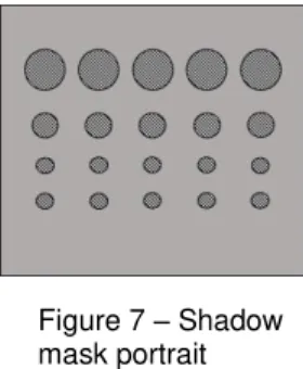
Shadow masks used for this work are portrayed in Figure 7. During this work, devices will be called Big, medium or small according to their size (Big devices have 1.8687 mm diameter, medium ones have 0.8867 mm diameter and small devices have 0.3651 mm diameter). Shadow masks were maintained across all deposition steps in order to have a vertical configuration, avoiding MIS devices with a common
CT-layer. When gold nanoparticles were deposited no shadow masks were used when forming the monolayer, after that process shadow masks were used as in molybdenum samples.
3.5. Electrical and layer characterization
For topographic images a scanning electron microscope was used, the equipment was a Carl Zeiss Auriga model. Allowed to check particle density and layer uniformity.
Nanoparticles as a charge trapping layer in
Metal-Insulator-Semiconductor structures 15
For thin film thicknesses a perfilometer and ellipsometer were used. The models for both machines are respectively an Ambius Xp-200 and a Sobin Yvon Uvisal spectroscope. Ellipsometer
measurements were executed at 70º.
To perform electrical characterization of the devices a semiconductor characterization system was used (Keithley 4200 SCS). C-V, C-F and I-V curves were the electrical characterization methods used.
One of the upsides of using this kind of measuring equipment is the high impedance, having high impedance on the input when using voltage sweeps allows for precise values of the input voltage and reliable results. For all the measurements the setup used was two tips, one at the top contact and the other at the bottom contact, bottom contact is usually grounded. For the kind of measurements performed, the most important values to have into account available with the equipment are the voltage sweep, the step voltage, frequency of measurement and AC level.
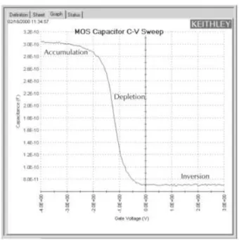
Of all the measurements made, C-V measurements are the main characterization curves in this work. Figure 8 shows the main regions of a C-V curve in a p-type MIS structure.
Figure 8 - C-V curve on Keithley as seen in [15]
Nanoparticles as a charge trapping layer in
Nanoparticles as a charge trapping layer in
Metal-Insulator-Semiconductor structures 17
4. RESULTS AND DISCUSSION
For the analysis of devices developed during this work, mainly electrical characterization was executed. In MIS structures C-V curves are the principal method used to understand the behavior of the devices. Non-electrical characterization was done to complement the electrical study, while giving an idea of the structure obtained during fabrication.
4.1. Ellipsometry, Profilometry and SEM analysis
Ellipsometry was the chosen method to obtain thicknesses of the tunneling SiO2 layer since it allows to assess optical and structural properties of very thin films such as these (<10 nm). To obtain the film thickness, a model for RTA growth of silicon oxide was used. The energy sweep was between 0.59 to 6 eV. Different samples with and without the RTA grown oxide were measured in order to test measurements.
Thicknesses of the Parylene thin films were obtained with a porfilometer, and ellipsometry. Thicknesses measured were around 150 nm.
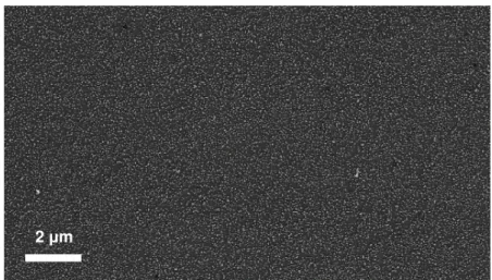
Topographic analysis via SEM was done after nanoparticle deposition, this step helped obtaining the spatial density of the nanoparticles, using Manuel et al. process [14], spatial densities around 109 particles/cm2 were obtained. As in [5][9][11][14-15], it is generally recommended a spatial density of 1012 particles/cm2, but it has been reported , working devices with lower particle densities. Figure 9 shows the SEM image that was used to calculate particle density.
Figure 9 – SEM image of particle distribution using Manuel et al. deposition method.
Nanoparticles as a charge trapping layer in
Metal-Insulator-Semiconductor structures 18
Higher particle densities could be obtained if smaller nanoparticles were used. A method to fabricate a higher spatial density film was also tried in this work using reported processes [11][16-17], where a thin metallic film(~6nm) was deposited and followed by RTA treatments. However, we found an un-homogeneous film and measured devices with the RTA surface treatment had not shown any charging behavior.
4.2. Tantalum oxide as a dielectric layer
At the start of this work, the blocking dielectric was chosen. Ta2O5 with different ratios of SiO2 is one of the most used dielectrics on CENIMAT and therefore a good option for the blocking oxide. In order to make a decision on tantalum as a dielectric for the blocking layer or as a multicomponent Ta-Si-O, electrical characterization of MIS structures was executed. The devices were deposited on p-type Silicon. Top and bottom contacts were made from evaporated Aluminum.
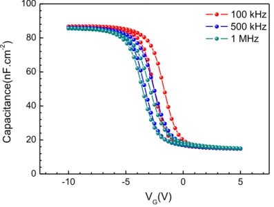
-10 -5 0 5
0 20 40 60 80 100 100 kHz 500 kHz 1 MHz C a p a c it a n c e (n F .c m -2 )
VG(V)
Figure 10 – C-V characteristic of a Ta2O5 MIS structure. Ratio 100/0 Tantalum/SiO2, AC Level 25 mV and 0.3 V step size
Nanoparticles as a charge trapping layer in
Metal-Insulator-Semiconductor structures 19
changes might suggest that interface defects are present in tantalum oxide and their influence is enhanced by being subject to electrical stress.
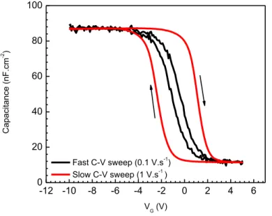
-16 -12 -8 -4 0 4 8
0 20 40 60 80 100 C a p a ci ta n ce (n F .cm -2 ) V G(V)
-6 -4 -2
0 100 Ca paci tance ( nF .c m -1) Bias (V)
Figure 11 – Transition voltage shift on a tantalum oxide MIS for consecutive measurements with an AC Level of 100 mV and at 1 MHz.
-12 -10 -8 -6 -4 -2 0 2 4 6
0 20 40 60 80 100
Fast C-V sweep (0.1 V.s-1)
Slow C-V sweep (1 V.s-1 )
C a p a ci ta n ce (n F .cm -2 ) V G (V)
Nanoparticles as a charge trapping layer in
Metal-Insulator-Semiconductor structures 20
The behavior observed for tantalum samples despite interesting, it is a downside when trying to analyze the behavior of a CT-layer, the possibility of masking the CT-layer charging/discharging makes Ta2O5 not a good solution for this work.
The stability of C-V curves and low leakage is an upside of this dielectric, joined with the charging behavior it presents, usage of Ta2O5 as a CT-Layer is to be studied in future work. Some reports have already proposed Ta2O5 for memory applications [20].
Co-sputtered oxides of mixtures of Ta2O5 and SiO2 were also tested as dielectric layer with different tantalum to silicon oxide ratios. Different RF power was applied to the SiO2 target in order to achieve the different SiO2 ratio in the dielectric films.
With the objective of seeing the variation of capacitance and dielectric constant of different deposition parameters, C-V analysis was executed. In Table 1, the results for 6 different Ta2O5:SiO2 ratios are present.
Ta2O5/SiO2(Deposition Power W/W) Name C/A(nF/cm2) Κ |Vfb shift|(V)
100/0 TS0 79.6 23.38 1
50/150 TS2 82.7 9.14 0.8
75/150 TS3 49.6 9.19 0.2
100/150 TS4 50.7 10.70 0.3
125/150 TS5 59.7 12.20 0.4
150/150 TS6 118 23.73 0.3
Table 1 – Tantalum oxide C-V details for diferent thicknesses of oxide and diferent oxide to silicon dioxide ratios.
In Table 1 the flat band voltage shift is the hysteresis value for in the devices with specific deposition conditions.
Nanoparticles as a charge trapping layer in
Metal-Insulator-Semiconductor structures 21
4.3. Parylene as a dielectric layer
With the objective of understanding Parylene as a candidate for the blocking layer, MIS structures were tested and C-V curves of Parylene with different adhesion promotors were measured.
-4 -2 0 2 4 6 8 10 12 14
0,6 0,7 0,8 0,9 1,0 C /C M A X
VG(V)
No promotor Liquid promotor Gas promotor
Figure 13 – C-V curve Parylene without CT-layer. Measurement performed at 500 kHz. Ac level 100 mV
Stability was one characteristic seen in this devices, overall they achieved a good performance and no hysteresis is seen Figure 13. Even though the devices are stable, they show a problem when reaching higher values of inversion or accumulation, they usually break, forming artifacts in both areas. This is the reason for Figure 13 presenting different Voltage sweep values. In the figure is seen as well the influence of the adhesion between Parylene and Silicon in the C-V curves obtained, different promotors show a change in flat-band voltage. In Table 2 the influence of different promotors in the capacitance is seen.
The transition voltage shift that occurs in every device tested is thought to be caused by the interface between Parylene and its contacting layers. Being an organic material, interfaces are inevitably imperfect and defects across those interfaces are highly probable to have an influence on shifting C-V curves. Defects can be present across the dielectric as well, charges trapped across the film are not unusual and have been reported in different works where Parylene is used as a blocking layer [9][19].
Nanoparticles as a charge trapping layer in
Metal-Insulator-Semiconductor structures 22
voltage shift. One possible reason for this kind of results is the trapping sites and defects caused by the presence of an organic layer created by the adhesion promotors [9]. However the yield obtained for devices without adhesion promotor is smaller than with it. As the number of devices measurable with promotor was greater, it was made the decision to keep using adhesion promotor.
Small Samples Average CMAX(F) C/A(F/cm2) Frequency(Hz) κ
No promotor 2.15x10⁻¹¹
1.41x10-08
20000 2.88
Liquid promotor 2.48x10⁻¹¹
1.62x10-08
20000 2.96
Vapor phase promotor 3.52x10⁻¹¹
2.30x10-08
20000 3.02
Table 2 – Maximum capacitance registered for devices with diferent promotor deposition methods at a fixed frequency.
Table 2, shows the variability of the maximum capacitance with the type of adhesion promotor, allowing to make some considerations about its influence in electrical characteristics of Parylene. Maximum capacitance is reached when the vapor phase promotor is used, it may be due to a better promotor to SiO2 adhesion, nevertheless, with any method of promotor used, capacitance over area values are around the same range giving the idea that in terms of measured capacitance it is indifferent which type of promotor is used. It was made the choice of using mainly vapor phase promotor since devices with no promotor had far less measurable devices.
Nanoparticles as a charge trapping layer in
Metal-Insulator-Semiconductor structures 23
-2 0 2 4 6 8 10 12 14 16 18 20
0,6 0,7 0,8 0,9 1,0 C /C M A X
VG(V)
500 kHz 100 kHz 20 kHz 5 kHz
Figure 14 – Parylene samples with no CT-layer. In order, measurements were made with a sweep between [-2,20] AC level 100 mV
The expected C/CMAX at inversion is around 0.6, but some devices have higher inversion capacitance. As reported in [9], the high capacitance values at inversion are generated from organic layers created during deposition.
4.4. C-V Details for MIS with CT-Layer
Double sweep C-V curves in devices with a CT layer show a shift in flat-band voltage when charges are stored, in this devices AUNP and metallic layer show hysteresis during the sweep while reference samples show no hysteresis. It is reasonable to say that the presence of a layer between Parylene and silicon dioxide is increasing the device ability to store charges [14][16][20-21].
Two important details about the measurements is the AC level used. (100 mV). AC levels unusually high
may prevent minority charge movement if those charges can’t follow the AC voltage(AC level in Keithley is given by a Vrms value). That was not the case, and to add, low frequency C-V measurements were even obtained [24].
Nanoparticles as a charge trapping layer in
Metal-Insulator-Semiconductor structures 24
was able to be measured. Nevertheless, measurements at 500 kHz were able to be made except when AUNP were used and some results are shown at these frequencies.
Frequency dependence of C-V curves comes from different responses of mobile and trapped charges between the interface region and the bulk of the semiconductor. The type of charges has some influence as well in the frequency at which measurements are made, holes have low responsivity to frequencies higher 100 kHz and possibly the reason for not being able to make C-V measurements when hole movement is crucial for device performance [21].
4.5. Molybdenum as a CT-Layer
When trying to achieve a device where tunneling to a charge trapping layer occurs, work functions of the semiconductor and metallic layers have to be taken into account. Dielectric properties should also be taken into account, a defect less dielectric is the end goal for tunneling layers. In this case, as mentioned in other instances of this work, dielectric and semiconductor are standard as tunneling layer and substrate for this kind of devices, it is assumed the interfacial layer between both tunneling dielectric and semiconductor has minimal defects. Metal films have a benefit comparing with other charge trapping layers, the ability to tune the work function to the desired value has the utmost importance when this kind of layers are used. Molybdenum has a higher work function than silicon, around (4.5,4.8)eV, this work function allows charges to tunnel to the trapping site and stay there since they will require a counter electric field to tunnel back [15].
Measurements were made from inversion to accumulation and step was adjusted in order to have a stable inversion capacitance. The expected results are electron trapping in the device, at the inversion; charges should tunnel from the inversion region to the molybdenum layer [15] and when sweeping to negative values a counter clock-wise hysteresis is expected; in fact it is reported that counter clock-wise loops are due to electron trapping [23]. Inversion electrons from the Si substrate enter the molybdenum layer through tunneling. When accumulation is reached, accumulation holes start to tunnel from the substrate and occupy previous electron trapped states in the film. An increase in sweep interval should show increasing hysteresis.
Nanoparticles as a charge trapping layer in
Metal-Insulator-Semiconductor structures 25
-5 -4 -3 -2 -1 0 1 2 3 4 5
0,7 0,8 0,9 1,0 C /C M A X
VG(V)
[2,-1]V [2,-2]V [3,-3]V [4,-4]V [5,-5]V [5,-5]V
Figure 15 – C-V for Molybdenum as a CT-Layer.Measurements executed at 500 kHz, AC level of 100 mV and step 0.25 V . Small device size. Clockwise hysteresis is identified which
suggests hole trapping
-7 -6 -5 -4 -3 -2 -1 0 1 2 3 4 5 6 7
29,5 30,0 30,5 31,0 31,5 C (p F ) V G(V) [1,-1]V [2,-2]V [3,-3]V [4,-4]V [6,-6]V
Figure 16 – C-V from a device with Molybdenum as a CT- Layer. Measurement at 500 kHz, 100 mV AC level and 0.2 V step size. Small device size. This sample shows a counter-clockwise
hysteresis that suggests electron trapping
Nanoparticles as a charge trapping layer in
Metal-Insulator-Semiconductor structures 26
explain a lower hysteresis when hole trapping is detected. While the number of devices showing charging behavior was not enough to make a statistical analysis of the charging type of molybdenum, hole trapping was the most common method of charge trapping in the devices observed.
4.6. Gold nanoparticles as a CT-Layer
Using nanoparticles as a charge trapping layer, turned out showing decent hysteresis loops with different voltage sweeps. Like molybdenum, having a high work function metal in the CT-Layer and high electron affinity resulted in noticeable hysteresis [4-5].
In Figures 17 and 18, it is noted that on consecutive measurements a transition voltage shift is measured. In references [9] and [21], this voltage shifts are reported to happen when interface defects or bulk defects are present in the insulator, in this case, not having an UVO or other chemical treatment after nanoparticle deposition, affects the shift but the stress when applying voltage is also having an effect in the samples. Also, the C/CMAX ratio can be improved if the UVO treatment is applied [9]. It is important to control the organic layers deposited in the device, both in the nanoparticles as in the molybdenum, adhesion promotor for Parylene and nanoparticles has a huge role in device performance.
-16 -14 -12 -10 -8 -6 -4 -2 0 2 4 6 8
22 24 26 28 30 32 34 36 C (p F )
VG(V)
[-4,-10] [0,- 12] [2,-15] [6,-15]
Nanoparticles as a charge trapping layer in
Metal-Insulator-Semiconductor structures 27
-14 -12 -10 -8 -6 -4 -2 0 2 4
18 20 22 24 26 28 30 32
C
(p
F
)
VG(V)
[1, -19] [4, -22] [6, -25] [0, -5] [0,-5]
Figure 18 - Device with AUNP as a CT-Layer. Measurements at 20 kHZ, 100 mV AC level and 0.25 V step. Small device size. Clockwise hysteresis that suggests Hole trapping
Nanoparticles as a charge trapping layer in
Metal-Insulator-Semiconductor structures 28
-5 -4 -3 -2 -1 0 1 2 3 4 5
0,6 0,7 0,8 0,9 1,0
C
/C
ma
x
V(V)
[5,-5]V MOLY [5,-5]V AuNP
Figure 19 – Comparison between 2 samples with different CT-layers.
Comparing each graph in Figure 19, the ratio between the inversion capacitance on the AuNP CT-layer is higher than in molybdenum. As was talked before, this detail originates from not cleaning the organic residues after the AuNP deposition [9]. The slope at the flat-band voltage of MIS devices usually gives an idea of interface quality of the devices used, influence of the interfaces is particularly significant when trap states have discrete energy levels and is mostly seen at the flat-band voltage [21]. This detail suggests that defects at the Parylene interfaces are present, possibly between Parylene/metal or Parylene/CT-layer.
4.7. Inversion on devices with Molybdenum as a CT-layer
In the process of measuring these devices, experiments for lower frequencies were made to see the device behavior at those parameters. Some molybdenum devices showed a low frequency behavior, this type of behavior happens in silicon devices below 2 kHz and, depending on the doping, it can be measured at even higher frequencies [21][26]. During this work measurement of low frequency curves were made for frequencies in the range of 5 to 100 kHz and an explanation is proposed for that fact.
Nanoparticles as a charge trapping layer in
Metal-Insulator-Semiconductor structures 29
Figure 20 shows a schematic that illustrates the mechanism of peripheral inversion [26].
Figure 20 – Schematic for peripheral inversion as explained in [26].
In [26], rapid thermal processing is described as a possible reason to create conditions for surface charges to appear in the oxide and cause peripheral inversion.
The presence of an oxide surface charge with the same polarity as the substrates doping, promotes minority carrier movement to the substrate oxide/substrate interface and create an inversion region, the inversion enables easier measurement of low frequency-curves.
Nanoparticles as a charge trapping layer in
Metal-Insulator-Semiconductor structures 30
Knowing the influence of frequency on charge movement in the devices, it is possible to understand the importance of near interface charges, when low frequency curves at higher than 2kHz frequencies are being measured.
In devices affected by peripheral inversion a strong dependence on frequency is expected, in Figures 21 and 22 it is possible to see the development of inversion capacitance with frequency.
-7 -6 -5 -4 -3 -2 -1 0 1 2 3 4 5 6 7
0 100 200 300 400 500 600 700 C (p F )
VG(V)
[5,-5] 5 kHz [7,-7] 5 kHz [7,-7] 20 kHz [7,-7] 100 kHz
Figure 21 - C-V curves at different frequency of a sample with Molybdenum as a CT-Layer. Big device size.Step 0.25 V 100 mV AC level
1000 10000 100000 1000000 1E7
0 100 200 300 400 500 600 700 C (p F ) f(Hz)
[1kHz, 10 MHz] 7 V
Nanoparticles as a charge trapping layer in
Metal-Insulator-Semiconductor structures 31
With the results obtained it is possible to note that peripheral inversion is a possible reason for low frequency curves to be measured. In future work a study of the area dependence of peripheral inversion on these devices is a great step to understand this kind of behavior.
In Figure 23, we study if accumulation needs to be reached in order to see a “hysteresis” loop in inversion. No loop was detected. This detail shows that the loop seen in the inversion region (Figure 20) is not caused by any charging or discharging of the CT-layer. The capacitance measured is the insulator capacitance of the device and means that an inversion layer is created and only when accumulation is reached the minority carriers leave the depletion region.
-1 0 1 2 3 4 5 6
0,1 0,2 0,3 0,4 0,5 0,6 0,7 0,8 0,9 1,0
-2 -1 0 1 2 3 4 5 6 7 8 0,1 0,2 0,3 0,4 0,5 0,6 0,7 0,8 0,9 1,0 C /C M A X
VG(V)
[3,-1] [5,-1] [6,-1]
VG(V)
[6,-2] [7,-2] [8,-2]
Figure 23 - C-V curves for varying sweep intervals without reaching accumulation for devices with Molybdenum as a CT-layer. Small device size. Measurements at 10 kHz, step size of 0.25
V and AC level of 100 mV.
Nanoparticles as a charge trapping layer in
Metal-Insulator-Semiconductor structures 32
In Figure 24, forward sweep slopes at the inversion are numbered in no specific order, just for simplicity and to be relatable to the C-t graph. The capacitance over time plot shows the development of the capacitance of the device at 1 volt, with the objective to see how the Capacitance measured develops with a small bias. Previous to this measurement a positive bias in accumulation is applied to bring the capacitance measured closer to position 1 in the C-V example.
0 100 200 300 400 500 600 700
-10 -9 -8 -7 -6 -5 -4 -3 -2 -1 0 1 2 3 4 5 6 7
0.0 0.1 0.2 0.3 0.4 0.5 0.6 0.7 0.8 0.9 1.0 1.1 7 4 7 V 1 V C (p F ) Time(s) [1,3] 6 5 3 1 C /C M A X V G(V) [7,-4]V [7,-5]V [7,-6]V [7,-7]V [7,-8]V [7,-9]V [7,-10]V 2 4 5 6 7
Figure 24 –C-t curve for a device with Molybdenum as a CT-layer. Superimposed frequency of 10kHz with 100 mV AC level. Small device size. Development of capacitance with bias applied
to the device, shows the importance of minority carriers in low frequency C-V curves. C-V curves for varying sweep intervals for a device with Molybdenum as a CT-layer. Small
device size. Measurements at 10 kHz, step size of 0.25 V and AC level of 100 mV.
4.8. Study of current through Silicon dioxide
With the goal of identifying current characteristics of silicon dioxide in this structure, some I-V measurements were executed. When thicknesses around 8 nm are present, it is reasonable to say Fowler-Nordheim tunneling is predominant in this device. Some tests are then executed to check the influence of applied voltage in stress induced leakage [8].
The next plot (Figure 25) is a Fowler-Nordheim plot (J/E2 vs 1/Eox), with this plot, a linearity is to be expected if Fowler-Nordheim tunneling is occurring, this linear plot comes from equation.1 that describes current density when Fowler-Nordheim tunneling is present.
𝐽𝐹𝑁= 𝑎𝐸𝑜𝑥2 𝑒𝑥𝑝 [−𝑏
Nanoparticles as a charge trapping layer in
Metal-Insulator-Semiconductor structures 33
𝑎 and 𝑏 are constants, by the equation it is noted that a negative slope should be noted in a Fowler-Nordheim plot.
0,10 0,11 0,12 0,13
10-27 10-26 10-25 10-24 10-23 10-22 J/ Eox 2 (A. V -2 ) 1/E ox(cm.MV -1 )
Figure 25 – Fowler-Nordheim plot of a MIS structure with SiO2 grown by RTA as the dielectric. The I-V curves that originated this plot had a sweep interval from -8 V to 8 V.
Figure 25 shows that a linear correlation between 1/Eox and J/Eox2 is obtained which suggests that Fowler-Nordheim tunneling is present in this devices and possibly in the MIS structures with a CT-layer. For lower electric fields it is reported a non-linearity that is present in similar structured devices, Despite not being shown in the plot, the non-linear behavior was seen [6]-[7].
As it was mentioned before, trap assisted tunneling is a reality, especially if it brings into account the stress induced defects in the silicon and sometimes in Parylene. An analysis of current in the device at different temperatures can show if trap assisted tunneling is present. It is expected, as reported in [6], an exponential decrease in current for higher temperatures in a J-Eox2 plot, the results show otherwise [6]. The expected decrease in current comes from the Frenkel-Poole description of the thermal excitation of trapped electrons into the oxide conduction band [6] as follows
𝐽𝐹𝑃= 𝑐𝐸𝑜𝑥𝑒𝑥𝑝[((𝑑𝐸𝑜𝑥)1/2− ф
𝑡)𝑞/𝑘𝑏𝑇] (2) Where 𝑐 is a constant that depends on trap density, 𝑑 is a constant related with the permittivity of the
Nanoparticles as a charge trapping layer in
Metal-Insulator-Semiconductor structures 34
When reviewing Figure 26, the exponential correlation of current with the square root of the oxide is not shown, currents increase with temperature which means that trap-assisted tunneling is not predominant in the devices. This results are interesting because they corroborate the fact that the SiO2 has a low number of defects, low enough that the current on the device in the J-Eox2 plot does not show thermally activated current of trapped electrons in the device [6]. Although we can reach a conclusion of the low quantity of defects in the oxide, it is not possible to assure that stress induced defects are not being created in the oxide and therefore SILC can be present in the MIS with CT-layer structured samples.
1000 2000 3000
10-7
10-6
10-5
10-4
J(A/
cm
2 )
E1/2ox(MV/cm)1/2
25 45 65 85
Figure 26 – Plot of current density versus square root of the oxide electric field for diferent temperatures in order to check temperature dependence on tunneling from the oxide
Nanoparticles as a charge trapping layer in
Metal-Insulator-Semiconductor structures 35
5. CONCLUSIONS AND FUTURE PERSPECTIVES
During this chapter, some thoughts will be presented regarding the results obtained and where they will lead. An extensive analysis on nanoparticles was not possible, time constraints did not allow a deep understanding of every process resulting from the presence of nanoparticles. Nevertheless, it was possible to see the charging behavior of different CT-layers and characterize it.
5.1. Conclusions
Following this thesis organization, some conclusions over device fabrication will be shared followed by analysis on blocking oxides and CT-layers.
As seen in the results obtained, interfaces between layers have a huge role in the electrical performance and cause non-controllable artifacts that can mask the CT-layer charging and discharging. UVO treatments should have been performed to improve AuNP interface with Parylene, as it seems to be one detractor in device performance. When depositing Parylene, the control of the adhesion promotor has to be taken into account, results showed vapor phase promotor deposition to be more stable in this devices.
Testing Ta2O5 allowed to understand the role of blocking oxides in this kind of devices, the importance of not allowing charge transport from the gate to the CT-layer and resistance to stress induced defects. Adding to the last point, the polarizing nature of Ta2O5, may be interesting to memory devices but in the scope of this work, any masking effects by the blocking oxide can give the wrong idea of the role the CT-layer is displaying.
Nanoparticles as a charge trapping layer in
Metal-Insulator-Semiconductor structures 36
5.2. Future perspectives
As for future perspectives for this work study of Parylene adhesion for the different CT-layers is a step forward, decreasing interface defects will bring better performance with devices using Parylene as a blocking oxide.
The results for devices with AuNP as a CT-layer show us the potential for this kind of memory devices, an improvement on the current devices through investigation of alternative ways to deposit the nanoparticles should be taken into consideration. A method without using organic compounds to have the particle monolayer is a step in the right direction for good films to use as a CT-layer.
After having the fabrication process perfected, an electrical analysis of this devices have to be further investigated. The process of peripheral inversion has to be further studied, area influence on the process is not taken into account but it is an important detail in devices that are affected by peripheral inversion. Electrical characterization of Parylene has to be further studied as well, the effects of each promotor in the electrical performance of Parylene films is not yet fully understood.
The best way to use nanoparticles in the CT-layer is yet to be discovered, since processes of retaining charges and charge movement across the particles and surrounding layers are not fully understood finding the best configuration for the particle monolayer is difficult. Maximizing devices performance with CT-layer configuration has to be studied, nanoparticle size, particle density, different type of nanoparticles (different metals) or using metallic shells are areas that need further investigation.
Nanoparticles as a charge trapping layer in
Metal-Insulator-Semiconductor structures 37
6. BIBLIOGRAPHY
[1] M. She, “Semiconductor Flash Memory Scaling,” Thesis, 2003.
[2] J. Meena, S. Sze, U. Chand, and T.-Y. Tseng, “Overview of emerging nonvolatile memory technologies,” Nanoscale Res. Lett., vol. 9, no. 1, p. 526, 2014.
[3] T. Usuki, K. Tsunoda, A. Sato, T. Nakanishi, and H. Tanaka, “Direct tunneling memory,” Fujitsu Sci. Tech. J., vol. 39, no. 1, pp. 72–77, 2003.
[4] J.-S. Lee, “Recent progress in gold nanoparticle-based non-volatile memory devices,” Gold Bull., vol. 43, no. 3, pp. 189–199, 2010.
[5] D. Tsoukalas, P. Dimitrakis, S. Kolliopoulou, and P. Normand, “Recent advances in nanoparticle memories,” Mater. Sci. Eng. B Solid-State Mater. Adv. Technol., vol. 124–125, pp. 93–101, 2005. [6] J. Kolodzey, S. Member, E. A. Chowdhury, T. N. Adam, G. Qui, I. Rau, J. O. Olowolafe, J. S. Suehle, S. Member, and Y. Chen, “Electrical Conduction and Dielectric Breakdown in Aluminum Oxide Insulators on Silicon,” vol. 47, no. 1, pp. 121–128, 2000.
[7] T. Endoh, “A quantitative analysis of stress-induced leakage currents in ultra-thin silicon dioxide films,” vol. 00, pp. 958–963, 2001.
[8] M. Engg, “Thin Dielectrics for MOS Gate,” 1996.
[9] B. Park, K. J. Im, K. Cho, and S. Kim, “Electrical characteristics of gold nanoparticle-embedded MIS capacitors with parylene gate dielectric,” Org. Electron. physics, Mater. Appl., vol. 9, pp. 878–882, 2008.
[10] Christian Hollauer, “Modeling of Thermal Oxidation and Stress Effects,” p. chapter2.3, 2007. [11] W. He, S. Member, J. Pu, D. S. H. Chan, S. Member, and A. Lanthanum-based, “Performance
Improvement in Charge-Trap Flash Memory Using Lanthanum-Based High- κ Blocking Oxide,”
vol. 56, no. 11, pp. 2746–2751, 2009.
[12] C. Lee, J. Meteer, V. Narayanan, and E. C. Kan, “Self-assembly of metal nanocrystals on ultrathin oxide for nonvolatile memory applications,” J. Electron. Mater., vol. 34, no. 1, pp. 1–11, 2005.
![Figure 1 - Left picture is a conventional Flash memory with a floating-gate.Right picture is a charge trapping flash memory with a nano-floating gate.[4]](https://thumb-eu.123doks.com/thumbv2/123dok_br/16697072.743866/25.892.173.815.833.954/figure-picture-conventional-flash-floating-picture-trapping-floating.webp)