http://www.bipublication.com
Case Report
An Investigation of Impact of Transistor Gate’s Thickness of Floating Gate
Transistor in Improvement of Sensitivity of Low-Power
Gamma-Ray Dosimeters
1
Armin Afshari Moghaddam and 2Mohammad Javadian Sarraf
1
Department of electronics,KhorasanRazavi,Neyshabur, Science and Research branch,Islamic Azad university,Neyshabur,Iran
2
Department of Electrical Engineering, Mashhad branch, Islamic Azad University, Mashhad, Iran Corresponding author:Mohammad JavadianSarraf,
Email: [email protected],Tel: +989153109755
ABSTRACT:
Gamma-ray dosimeter is an instrument which measures dose amount attracted by gamma ray. This integrated sensor is utilized for high irradiation and low sensitivity applications such as blood sterilization. In this article, a gamma-ray MOSFET dosimeter including a floating-gate MOSFET transistor as a sensor and a gate connection reference transistor with identical geometry are simulated using the TSMC 0.13-micron process technology. Floating-gate transistor is used in low-power circuits. The dosimeter applied herein makes use of general dose measurement methodology. Source of gamma ray is cobalt-60. Here, the impact of transistor gate’s thickness of floating transistor served as a sensor on sensitivity of dosimeter is examined. To do so, dosimeter was simulated using the software HSPICE, and impact of different thicknesses of floating transistors on sensitivity was examined. Finally, it was concluded that an increase in transistor gate’s thickness of floating transistor would bring about an improvement of at least 25 percent in sensitivity.
Keywords:Gamma-ray dosimeter, floating gate,sensitivity, 0.13-micron, HSPICE
[I] INTRODUCTION
In this article, impact of transistor gate’s thickness of floating transistor on sensitivity in dosimeters is addressed. Floating gate is used to improve sensitivity for low-power circuits. It, in addition, is able to save loads and it is thus applied in memory cells [1]. Application of floating-gateMOSFET transistors as dosimeters for irradiation purposes is also examined [2], [3], [4] and [5]. These transistors might be manufactured in commercial analog CMOS technology. Floating-gate transistors are highly sensitive to X- and gamma-ray irradiations without needing an external BIOS source. Irradiation provokes electron-hole pairs in oxide around floating-gate, the event which causes depletion of gate (de-charging) and shift of
threshold. Keys to advancement of dosimeter (such as emergency, small size, low-power consumption, etc.) are due to their compatibility in applying CMOS modern and commercial technologies in their structures[6]. Sensitivity is an important parameter in dosimeters and constitutes one of the major concerns borne by researchers in designing dosimeters. At the beginning, floating gate was in 1996 used in designing dosimeters [7]. A new MOSFET-based dosimeter was presented that makes use of a polysilicon floating gate. The dose attracted in MOSFET presents itself through a change in threshold voltage.
chip,FGRADFET, had a non-floating reference and was placed on the other chip as op-amp that was responsible for rereading process [8]. First of all, Arsalan, PhD, managed to construct a dosimeter on a chip and placed readout component on the same chip. He used DALSA 0.8-micron process technology [9]. Yadegari utilized IBM 0.13-micron process technology in his design, and placed sensor component as a part of readout circuit. Moreover, he used floating gate extension to improve sensitivity [10].
Gamma-ray dosimeter is widely used in applications such as special explorations, food sterilization processes, monitoring nuclear facilities, radiation therapy, and many other applications in biomedical grounds. Blood sterilization by gamma and X rays is required for prevention from infections. Thus, anything which causes automation, improvement of qualitative performance, and reduction of expenses is required and regarded as important. Sensitivity brings about improvement of qualitative performance of dosimeters and increased range of their performance.
[II] DOSIMETER STRUCTURE OF
GAMMA RAY
In order to examine impact of transistor gate’s thickness of floating transistor on dosimeter’s sensitivity, another dosimeter circuit which was applied by other researchers was employed [10]. Simulations were conducted using the TSMC 0.13-micron process technology in the software Hspice.
The circuit is shown in the Fig. 1. This is mainly characterized by its low power, application of reference pair, and application of gate extensions to include all required range [10]. Dosimeter was constructed and sensitivity was obtained to be 0.4 mv/Gy[10]. Since this amount is measured by three small, medium, and large gate extensions and it is obtained using IBM technology, it cannot be equalized with sensitivity amount obtained from simulations (without changing thickness). On the other hand, we intend to improve sensitivity by changing thickness of floating gate; therefore, we simulate dosimeter with small gate extension, comparing sensitivity both before and after changing gate’s thickness. Results would naturally be generalizable for medium and large gate extensions.
Fig. 1: dosimeter circuit
2.1. Sensitivity in gamma-ray dosimeter
To determine sensitivity, we have the formula 1 [12]:
(1)
∆Vthis shift in threshold voltage through irradiation. D is attracted dose. For n=1, A presents sensitivity (s):
D is regarded to be equal to 854.4 gray [10]. Shift of threshold voltage is written as follows [13]:
(3)
The first term which is multiplied by
expresses reduced density, and the second term expresses reduction in mobile carriers in channel. The first term is an equation for impact of oxide traps on threshold shifts. is changes
in number of interface traps in oxide areas, and is changes in number of body oxide traps in
irradiation-caused oxide areas. In equation 3, + is used for nmos and for pmos is removed as
time elapses; while, is maintained and makes
the major cause for sensitivity [14]. Consider relation 4:
(4)
is dielectric constant and is thickness of
oxide layer. Filling in the relation 3, we have for pmos transistors:
(5)
is removed as time elapses. Thus, we have:
(6)
We have:
(7)
And, finally:
(8)
RD, L, W, , , and are constant. And,
is constant since we change thickness of
floating gate transistor in a fixed irradiation. Thus, we have:
(9)
Then:
(10)
, , and, are
constant. Using equations 2 and 10, we have:
(11)
Equation 11 is indicative of the relation between thickness and sensitivity as to attracted dose. It shows that sensitivity is increased as thickness is elevated.
2.2. Transistor modeling to be used in Hspice
Circuit modelFGRADFET or floating gate transistor that is subjected to irradiation, was simulated using [11]. Capacitor amount used is 300 Femto-Farad.
[III]SIMULATION OF DOSIMETER
This simulation includes the following stages: 1. Before irradiation
2. After irradiation:
a. Without changes in thickness and width ofFGRADFET
b. With changes in thickness of FGRADFET gate
c. With changes in width of FGRADFET
In this article, width of FGRADFET was examined in addition to examination of impact of thickness on sensitivity.
3.1. Manner of simulation
In Table 1, amounts of circuit components of Fig. 1 are addressed.
Components Unit value M1
W/L
l=1µ 40
M2 40
M3 40
M4 20
FGRADFET 20
M7 5
M8 5
M9 10
M6 W/L 1.5
R KΩ 1
C1 PF 2
Table 1: amounts of circuit’s elements
Table 2 shows amounts of voltage and current sources.
I1 Vss Vdd
µ 350 -1.2v 1.2v
Table 2: values of voltage and current sources
That is, for simulation purposes, impact of irradiation on floating gate transistor from a dc source in gate of this transistor was utilized. Since the factor to change loads is negative, source is regarded as negative.
Simulation was conducted. Value of output voltage before irradiation is 94.94 microvolts, which reaches to -149.9567 after irradiation. Graph 1 exhibits voltage values before and after irradiation without changing thickness of transistor gate, i.e., FGRADFET.
Graph 1: output voltage before and after irradiation
3.2. Examination of impact of gate’s thickness on sensitivity
Graph 2 shows a change in output voltage as thickness is increased. As observed, thickness starts from 2.85 nanometers and reaches 10.85 nanometers. Voltage starts from -149.9567 in thickness 2.85 nanometers, finally reaching to -716.9598 (in thickness of 10.85 nanometers). Primary value of thickness in 0.13 micron CMOS Library is 2.85 nanometers.
Graph 2: output voltage with changes in thickness after irradiation
Table 3 shows values of output voltage that are subject to changes as thickness of transistor is increased. toxis thickness of transistor of floating
gate and Voutis output voltage of dosimeter. In
Table 3, thickness is increased from 2.85 to 10.85 nanometers. And, voltage changes from-149.9567 to -716.9598.
tox(nm) Vout(mv)
2.85 -149.9567 3.85 -340.3308 4.85 -457.3527 5.85 -536.207 10.85 -716.9598
Table 3: values of output voltage with an increase in thickness of floating gate transistor
As specified in the Table 4, values ofFGRADFET thickness gate in terms of nanometers, sensitivity in terms of millivolts per gray, and threshold voltage in terms of millivolts. Sensitivities are calculated using relation 2 and general dose of ionization 854.4 gray. In Table 4, trend of thickness changes from 2.85 to 10.85 nanometers. Threshold voltage has changed from -442.998 to -47.665 millivolts, and sensitivity is improved from 0.02 to 0.436 millivolts/gray. Changes in readout circuit’s gain are also constant.
(nm) (mv) Gain
3.85 -317.068 0.1208 1.05 4.85 -236.380 0.2152 1.08 5.85 -180.512 0.2806 1.1 10.85 -47.6665 0.436 1.14
Table 4: calculated sensitivity values and gain and threshold voltage obtained from simulation as a result of increasing floating gate transistor’s thickness Graph 3 shows changes in sensitivity as thickness of floating gate transistor is increased. In Graph 3, thickness is changed from 2.85 to 10.85 nanometers, which indicates a sensitivity change from 0.02 to 0.436 millivolt/gray. Value of circuit’s output voltage after a reduction inFGRADFET was examined. It was concluded that transistors exit their areas and thus this is not creditable.
Graph 3: changes in sensitivity after an increase in floating gate transistor’s thickness
Graph 4 shows changes in
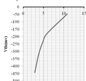
FGRADFETthreshold voltage after an increase in floating gate transistor’s thickness. In this graph, thickness is changed from 2.85 to 10.85 nanometers, showing a change in threshold voltage from -442.998 to -47.665 millivolts.
Graph 4: changes in threshold voltage after an increase in floating gate transistor’s thickness
3.3. Examination of impact of channel’s
width on
sensitivity
Graph 5 shows a change in output voltage after width is increased. As observed, width starts from 20 micrometers and reaches 100 micrometers. Additionally, voltage starts from -149.9567 millivolts in width of 20 micros and finally reaches -404.4731 in width of 100 micros. Primary width is 20 microns.
Graph 5: output voltage after a change in width after irradiation
Table 5 shows values of output voltage after width of FGRADFETis increased. In table 5, width of transistor is increased from 20 to 100 micrometers and output voltage is obtained by simulations from -149.9567 to -404.4731 millivolts.
W
(micron)
Vout
20 -149.9567
21 -161.3714
25 -199.6756
50 -320.1457
100 -404.4731 101 Not define
Table 5: values of output voltage after an increase in floating gate transistor’s width
Table 6 indicates values of threshold voltage (millivolts), sensitivity (millivolts/gray), and readout circuit gain after an increase in width ofFGRADFET (micrometers). Sensitivities are calculated using relation 2 and general dose as to be 854.4 gray. As per table 6, trend of changes in width is from 20 to 100 micrometers. And, threshold voltage is changed from -442.998 to -480.61 millivolts. Sensitivity, moreover, is improved from 0.0265 to 0.706 millivolts/gray. Changes in readout circuit gain are also almost constant.
W (micron)
Vth
(mv)
S (mv/Gy)
Gain
(Readout circuit)
20 -442.998 0.0265 1
21 -444.7188 0.0285 1.001 25 -450.4731 0.0353 1.006 50 -468.335 0.0562 1.018 100 -480.61 0.0706 1.025
Table 6: values of calculated sensitivity, gain, and threshold voltage obtained from simulations after an increase in floating gate transistor’s width
Graph 6 shows changes in sensitivity as width ofFGRADFET is increased. In Graph 6, width is changed from 20 to 100 micrometers, showing a change of sensitivity from 0.0265 to 0.0706 millivolts/gray.
Graph 6: changes in sensitivity as floating gate transistor’s width is increased
Graph 6 shows changes in threshold voltage as width ofFGRADFET is increased. In Graph 7, width is changed from 20 to 100 micrometers, showing a change of threshold voltage from-442.998 to -480.61 millivolts.
Graph 7: changes in threshold voltage as floating gate transistor’s width is increased
Table 7 shows values of output voltage as floating gate transistor’s width is decreased. When width is 10 microns, transistors exit from their areas, thereby voltage is not creditable with this width. Table 7 illustrates a reduction in width from 20 to 10 micrometers. Output voltage has been changed from 149.9567 to -75.8227 millivolts.
W(micron) Vout(mv)
20 -149.9567 19 -137.6099 18 -124.1991 17 -109.5661 15 -75.8227
10 *
Table 8 shows values of sensitivity and readout circuit gain after a reduction in floating gate transistor’s width. In this table, trend of changes in width is from 20 to 15 micrometers. And, threshold voltage is changed from -442.998 to -431.773 millivolts. In addition, sensitivity is changed from 0.02 to 0.0134 millivolt/gray. Changes in readout circuit gain are observed from 1 to 987.85 millies.
W
(micron)
Vth
(mv)
S (mv/Gy)
Gain (Readout circuit)
20 -442.998 0.02 1
19 -441.1339 0.0244 998.2772 milli 18 -439.1061 0.022 996.3133 milli 17 -436.8904 0.0194 994.0137 milli 15 -431.773 0.0134 987.8516 milli
Table 8: values of calculated sensitivity values and gain and threshold voltage obtained from simulation as a result of decreasing floating gate transistor’s width.
Graph 8 shows changes in sensitivity after a reduction in floating gate transistor’s width. Changes in floating gate transistor’s width have been from 20 to 15 microns. As observed, sensitivity changes from 0.02 to 0.0134 millivolts/gray.
Graph 8: changes in sensitivity after a reduction in floating gate transistor’s width
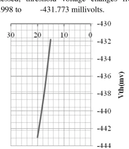
Graph 9 shows changes in threshold voltage after a reduction in floating gate transistor’s width. Changes in width of floating gate transistor have been from 20 to 15 microns. As
witnessed, threshold voltage changes from -442.998 to -431.773 millivolts.
Graph 9: Changes In Threshold Voltage After A Reduction In Floating Gate Transistor’s Width
[IV] DISCUSSION
Before irradiation, output voltage was -94.4 microvolts. After irradiation, however, output voltage reached -149.95 microvolts. Voltage difference is almost 149 microvolts. As observed in Graph 3, sensitivity is improved as trend of floating gate transistor’s thickness is increased. Simulations were done after thickness was reduced. While, these results are not reliable because transistors exit from their areas. Changes in sensitivity were considered as per an increase in width of gate (Graph 6). This is witnessed that increased width brings about an improvement in sensitivity. Reduction of width was, also, examined—the fact which causes a reduction in sensitivity, as seen in Graph 8. Additionally, readout circuit gain is not constant as width is decreased (Table 8). This is concluded that increase in thickness causes an increase in sensitivity, as foreseen from formulas. Even without consideration of obtained sensitivities and only by comparing size of changes in output voltages and by changing thickness of gate after irradiation as from that before irradiation, an improvement in sensitivity is observable.
[V] CONCLUSION
increased, in addition, there would be an 11-percent improvement in sensitivity as compared to the sensitivity gained by Yadegari. Increased thickness compared to increased width brings about a considerable improvement in sensitivity. Construction of this circuit with floating gate transistor with a thicker gate and also examination of impact of other components of floating gate on sensitivity and performance of circuit might be enumerated as future works.
REFERENCES
1. C. Wernli, A. Fiechtner, and J. Kahilainen, "The Direct Ion Storage Dosimeter for The Measurement of Photon, Beta and Neutron Dose Equivalents," Radiation Protection Dosimetry, vol. 84, no. 1-4, pp. 331-334, 1999.
2. N.G. Tarr, G.F. Mackay,"A Floating gate MOS Dosimeter Requiring No External Bias Supply", IEEE Trans. Nucl. Sci., Vol. 45, pp. 1470-1474, June 1998.
3. N.G. Tarr, C. Plett, etc, “Limitations on MOSFET dosimeter resolution imposed by 1/f noise”, IEEE Trans. Nucl. Sci., Vol. 43, pp. 2492 -2495, Oct. 1996.
4. N.G. Tarr, K. Shortt, Y. Wang and I. Thomson.,"A Sensitive Temperature-Compensated, Zero-Bias Floating Gate MOSFET Dosimeter", IEEETrans. Nucl. Sci., 2003.
5. Y. Wang and N.G. Tarr, etc.,"A Sensitive Floating Gate MOSFET Gamma Ray Dosimeter", IEEE Sensors 2003 Conference, Toronto, Canada, Vol. 2, pp. 1271-1276, 2003.
6. A. Holmes-Siedle, L. Adams, and G. Ensell, "MOS dosimeters- improvement of responsivity," in First European Conference on Radiation and its Effects on Devices and Systems, 1991. RADECS 91., New York, Sep 1991, pp. 65-69.
7. C.J. Peters, N.G. Tarr, K. Shortt, I. Thomson, and G.F. Mackay, "A floating-gate MOSFET gamma dosimeter," Canadian Journal of Physics, vol. 74, no. 12, pp.135-138,1996. 8. Tarr, N. G., Shortt, K., Yanbin, Wang, &
Thomson, I. (2004). A sensitive, temperature-compensated, zero-bias floating
gate MOSFET dosimeter. Nuclear Science, IEEE Transactions on, 51(3), 1277-1282. doi: 10.1109/TNS.2004.829372
9. Arsalan, M., Shamim, A., Shams, M., Tarr, N. G., & Roy, L. (2012). Ultra Low Power CMOS-Based Sensor for On-Body Radiation Dose Measurements. Emerging and Selected Topics in Circuits and Systems, IEEE
Journal on, 2(1), 34-41.
doi:10.1109/JETCAS.2012.2187404
10.Yadegari, B., Carleton University. Dissertation. Engineering, Electrical, & Computer. (2012). Low Power Gamma-ray FG-MOSFET Dosimeter in 0.13 Um CMOS Technology.
11.Saheb, Z. (2013). TRANSIT AND DC
MODEL OF FLOATING GATE
TRANSISTOR IN 90NM CMOS
TECHNOLOGY. (Masters Thesis). Dalhousie University. Retrieved from http://hdl.handle.net/10222/31441G.S. 12.Ristic, "Influence of ionizing radiation and
hot carrier injection on metal-oxide-semiconductor transistors," Journal of Physics D: Applied Physics, vol. 41, pp. 1-19, 2008.
13.K.F. Galloway, M. Gaitan, and T.J. Russell, "A Simple Model for Separating Interface and Oxide Charge Effects in MOS Device Characteristics," IEEETransaction on Nuclear Science, vol. 31, no. 6, pp. 1497-1501, Dec 1984.