JOURNAL OF NANO- AND ELECTRONIC PHYSICS Р А А - А Р
Vol. 7 No 2, 02029(4pp) (2015) Том 7 № 2, 02029(4cc) (2015)
2077-6772/2015/7(2)02029(4) 02029-1 2015 Sumy State University Extracted Electronic Parameters of a Novel Ag/SnO2:In/Si/Au Schottky
Diode for Solar Cell Application
Mostefa Benhaliliba
Material TechnologyDepartment,Physics Faculty, USTOMB University, BP1505 Oran, Algeria
(Received 19 February 2015; published online 10 June 2015)
The effect of indium on the characteristics of Ag / SnO2 : In / Si / Au Schottky diode (SD) is studied. The
electronic parameters, ideal factor, the effective barrier, flat band barrier height, the series resistance, the saturation current density of the diodes were extracted from the current voltage (I-V) and capacitance voltage (C-V) characteristics. The series resistance (Rs) determined by Cheung method increases (508-534 Ω) with In doping level while the barrier height still constant around 0.57 V. Norde approximation gives a similar barri-er height values of 0.69 V but the sbarri-eries resistance reaches highbarri-er values of 5500 Ω.
Keywords: Schottky diode, Tin oxide, Current-voltage measurements, Ideality factor.
PACS numbers: 85.30.Hi, 85.30.Kk
1. INTRODUCTION
During the last decades, the researchers in physics and electronics are interested by the performance and the microelectronics reliability of metal-insulator-semiconductor Schottky diodes particularly depend on the formation of an insulator film, active me-tal / semiconductor interface, and the interface states distribution at the semiconductor, insulator interface, series resistance and inhomogeneous barrier heights. Tin oxide (SnO2) belongs to the II-VI semiconductor family with a wide band gap of 3.5 eV [1-2]. It has been revealed that SnO2 is n-type direct band semiconductor and lately became a p-type material especially when it was doped with aluminum, zinc or indium [3-4]. Sever-al applications of SnO2 such as light emitting diodes and gas sensors have been mentioned [5-6]. In this re-search, we studied the electronic properties of indium doped SnO2 deposited onto a n-type silicon substrate by a low cost spray pyrolysis process. Thus, a Schottky diode has been fabricated and the current-voltage measurements have been achieved in dark and room temperature conditions. Besides, the capacitance-voltage were measured at various frequencies and the response has been plotted and several electronic pa-rameters have been extracted such as barrier height, series resistance, interface density and donor concen-tration. We study the role of indium level (6 and 8 %) as dopant on electronic and electrical properties of Ag / SnO2 / nSi / Au Schottky diode. We expect that this device will be used in optical sensors and solar cell.Our aim is the measurement and to make stronger the knowledge of conduction mechanism in such device based on the wide band gap oxides layers.
2. FABRICATION AND MEASUREMENTS
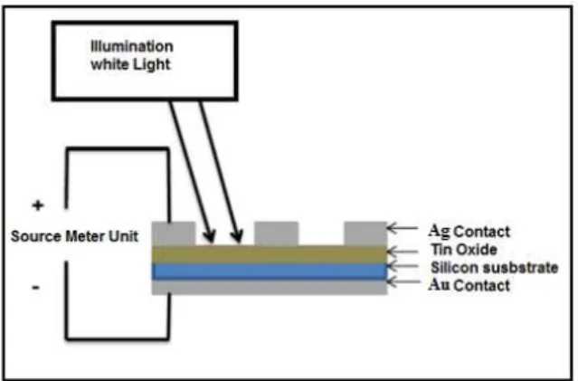
Sprayed at 300 °C, the films of tin oxide deposited on n type silicon were prepared by ultrasonic spray pyrolysis technique USP. Furthermore, the indium was incorporated at the amount of 6 and 8 % in the solu-tion. The gold contact, of thickness of 120 nm, was de-posited on the film by thermal evaporation at pressure of 1.5 10– 5 Torr. Using Keithley set up, the I-V char-acteristics under dark were measured. A schematic
cross-section of the Ag / SnO2 / nSi / Au structure is displayed in figure 1.
Fig. 1 –A schematic cross-section of the Ag / SnO2 / nSi / Au
structure
The electronic parameters, ideal factor, the effective barrier, the saturation current of the diodes were ex-tracted from the current voltage (I-V) characteristics. Indium doped SnO2 films were grown onto n-type sili-con substrate using ultrasonic spray pyrolysis route that was previously cited [1]. The contacts have diame-ter of 1 mm and thickness of 110 nm. The Ag / SnO2 : In / nSi / Au characteristics were measured using Keithley equipment. The voltage range varies between 0 and 5 V. The C-V data were taken at fre-quency of 100 kHz.
3. RESULTS AND DISCUSSIONS
Figure 2 depicts the semilog plotting versus bias volt-age which varies within (– 2, + 2) V for the Ag / SnO2 / Si / Au Schottky diodes. The measurements are achieved in dark conditions and at room temperature.
The exponential profile of the forward current-voltage characteristics depends strongly on the proper-ty of active material used for diode. It is given in terms of voltage and temperature as follows;
0 exp 1
qV
I I
nkT
MOSTEFA BENHALILIBA J.NANO-ELECTRON.PHYS. 7, 02029 (2015)
02029-2 Where V is the applied voltage, n is the ideality fac-tor is a quantity how the diode closes the ideal behav-ior, k is the Boltzmann constant, q is elementary charge, T is absolute temperature of 300 K and I0 is reverse saturation current. This latter goes from 227 to 748 nA.
The ideality factor of the as-fabricated diode is then given from
ln( )
q dV
n
kT d I
(2)
Where dV / dlnI is the derivative of voltage versus lnI, q is free carrier charge; T is the absolute tempera-ture, k 8.625 10– 5 eV/K is the Boltzmann constant. The ideality factor is found to be 2.7 and 3.6 respective-ly for 6 and 8 % indium doped SnO2 films, which con-firms the non-ideal behavior of the as-fabricated di-odes. A rectifying parameter is greater than 425 for the 6 % In doping level, but it is slighter for 8 % In doped tin oxide film.
Fig. 2 – Semilog Plot of current-voltage characteristics of Ag / SnO2 / nSi / Au Schottky diode for 6 and 8 % In doping
level
I0 can be obtained from the extrapolation of the lin-ear portion of semi-log I-V and is given by,
2 0
0 * exp
B q
I AA T
kT
(3)
Where A is the effective diode area, A* is the Rich-ardson constant and B0 the zero bias barrier height of the diode. A* is the Richardson constant (112 Acm– 2 K– 2 for n-type Si), [7], we calculated the value of AA*T2 80640.
The height barrier dependent on temperature and I0 is expressed as follows [14];
2
0 * ln
kT AA T
q I
B (4)
The H(I) function versus current is expressed as fol-lows [13],
2
( ) ln
*
nkT I
H I V
q AA T
(5)
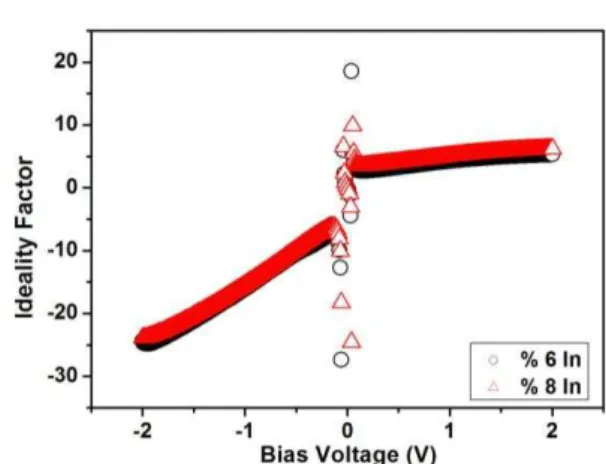
Fig. 3 – The ideality factor dependence on bias voltage of Ag / SnO2 / nSi / Au Schottky diode without Rs for 6 and 8 % In
doping level
Fig.4 – The capacitance-voltage plots of Ag / SnO2 / nSi / Au
Schottky diode for 6 and 8 % indium doping level
The capacitance-voltage plots of Ag / SnO2 / nSi / Au Schottky diode for 6 and 8 % indium doping level is shown in figure 4. This profile confirms the n type of the tin oxide layer. At the frequency of 100 KHz, 3.1 and 2.4 nF are the highest obtained value of the capaci-tance for the 6 and 8 % In doping level detected in the forward C-V characteristics. Capacitance increases rapidly with the bias voltage in the forward bias 0-5 V range. The 1/C2 versus bias voltage (0.2-0.7 V) is plot-ted as seen in figure 5. A straight line fitting of equa-tion, 1.5E19-2.1 E19 V and 1.3E19-1.76 V respectively for 6 and 8 % In doping level, permits to determine the donor concentration and the buit-in potential.
2 2
2( )
1 bi
d
V V
C q A N
(6)
And function H can be expressed in terms of barrier height and series resistance Rsby eqn. 5, and in terms
of barrier height and series resistance by the following relation;
( ) B s
H I n R I (7)
EXTRACTED ELECTRONIC PARAMETERS OF A NOVEL… J.NANO-ELECTRON.PHYS. 7, 02029 (2015)
02029-3 follows;
2 ( )
( ) ln
*
V kT I V
F V
q AA T
(8)
Where is the first integer greater than ideality factor. F(V) allows to determine Rs and ΦB as listed
below using the minimum voltage V0 and F(V0) (not shown here). The barrier height is then given by,
0 0 ( ) B
V kT
F V
q
(9)
The series resistance of the contact can be defined through the relation [8],
min S
kT n
R qI
(10)
The logI-logV curves identify two distinct current regions I and II (not shown here). Current obeys the power law of I ≈ kVm [7] where k is a constant and m is
the constant that describes the dominant conduction mechanism of the diode, Current-voltage characteris-tics and the power-law dependency were found to be ruled by a space charge-limited currents SCLC (slope m 2) because logI-logV plots give roughly the power laws as IV2.5 for the region II while the relation is modified as IV1.3 for the region I which confirms the ohmic regime. To explain the conduction mechanism of the Ag / SnO2 : In / Si / Au SD under high voltages;
Fig. 5 – 1/C2 vs. bias voltage plot of Ag / SnO2 / nSi / Au
Schottky diode for 6 and 8 % In doping level
The ideality factor versus bias voltage is given by [9-10],
( ) 1 s
ss i
n V qN
d
(11)
Where ε is a dielectric constant of SnO2 and silicon (I 70, s 11.8 0, where 0 8.84 10– 12 F/m). Based on the 1/C2 vs. V plots, the as-fabricated diode presents p-type conductivity. Acceptor density NA is assessed at
3.5 1014 cm– 3. Ideality factor dependence of interface states densities were obtained using eqn. 12 [10]. We determine the energy distribution of the interface states in equilibrium with semiconductor using the equation 12 and 13 by taking into account the forward bias current-voltage characteristics. The obtained val-ues of electronic parameters as a result of In doping level are gathered in Table 1.
1
( ( ) 1)
i s
ss
N n V
q d
(12)
Where n(V) is the ideality factor expressed by the eqn. 14 can be calculated with and without the series resistance Rs.
( )
ss V B
E E q V (13)
0 ( )
ln( ) s
V IR
q n V
I kT
I
(14)
The ideality factor dependent on current and bias voltage n(V) without Rs for 6 and 8 % In doping level is
sketched in figure 3. The interfacial layer thickness is deduced from the relation Ci i 0A/ [7]. The interface state energy density Nss,expressed by eqn. 12, is
plot-ted with and without series resistance for the 4, 6 and 8 % In-doped tin oxide as shown in figure 6.
Fig. 6 – The energy distribution profile of the interface state densities Nss obtained from forward I-V characteristics of
Ag / SnO2 / nSi / Au Schottky diode for 6 and 8 % In doping
level without Rs
Table 1 – Microelectronic parameters of Ag / SnO2 / nSi / Au Schottky diode for 6 and 8 % In doping level
In % n R I0
(10– 7 A)
Cheung meth-od using
dV/dlnI
Cheung meth-od using H(I)
Norde method F(V)
n Rs
(Ω) R(Ω) s Φ(V) B
V0 (V)
F(V0) (V)
Rs
MOSTEFA BENHALILIBA J.NANO-ELECTRON.PHYS. 7, 02029 (2015)
02029-4 4. CONCLUSION
The layer of indium doped tin oxide, as a part in the Ag / SnO2 : In / Si / Au Schottky diode, properties are completely studied.
Further, the effect of indium level on the electronic extracted parameters like ideality factor, saturation current, barrier height, series resistance is fully em-phasized. Based on I-V plots, we determine series sistance by Cheung and Norde methods and it is re-vealed that a non-ideal behavior of SD is observed (n is greater than unity). The obtained value of the satura-tion current I0 ranged within 220-750 nA. In doping level arises the series resistance in the diode in the
ratio of 1.5 while the barrier height stills the same around 0.57 V according to Cheung model. The energy distribution profile of the interface state densities de-creases with an increase in In doping level.
ACKNOWLEDGMENT
This work is a part of CNEPRU project N° D01920120039 supported by High Teaching and Scien-tific Research Ministry www.mesrs.dz and Oran Uni-versity of Sciences and Technology www.univ-usto.dz. The authors are grateful for the assistance of The Head and staff of the virtual library of SNDL https://www.sndl.cerist.dz.
REFERENCES
1. C.E. Benouis, M. Benhaliliba, F. Yakuphanoglu, A. Tiburcio Silver, M.S. Aida, A. Sanchez Juarez, Synthet-ic Metals161, 1509 (2011).
2. M. Benhaliliba, C.E. Benouis, Y.S. Ocak, F. Yakuphanoglu,
J. Nano- Electron. Phys.4 No 1, 01011 (2012).
3. C.E. Benouis, M. Benhaliliba, Z. Mouffak, A. Avila-Garcia, A. Tiburcio-Silver, M. Ortega Lopez, R. Romano Trujillo, Y.S. Ocak, J. Alloy. Compd.603, 213 (2014).
4. J. Miao Ni, X.J. Zhao, J. Zhao, J. Inorg Organomet Polym.
22, 21 (2012).
5. Sangyub Ie, Ji-Hwan Kima, Byeong Taek Bae, Dong-Hee Park, Ji-Won Choi, Won-Kook Choi, Thin Solid Films517,
4015 (2009).
6. T. Rui-qin, G. Yan-Qun, Z. Jun-hua, L. Yue, X. Tie-feng, S. Wei-jie, Trans. Nonferrous Metal Soc. China21, 1568 (2011).
7. S.M. Sze, K.K. Ng, Physics of Semiconductor Devices, Third ed. (John Wiley & Sons: New Jersey: 2007). 8. H. Norde, J. Appl. Phys.50, 5052 (1979).
9. E.H. Rhoderick, R.H. Williams, Metal-Semiconductor Con-tacts (Clarendon: Oxford: 1988).