JOURNAL OF NANO- AND ELECTRONIC PHYSICS Р А А - А Р
Vol. 5 No 2, 02001(3pp) (2013) Том 5 № 2, 02001(3cc) (2013)
2077-6772/2013/5(2)02001(3) 02001-1 2013 Sumy State University
Characterization of GaN Nanorods Fabricated Using Ni Nanomasking and Reactive Ion Etching: A Top-Down Approach
Ashutosh Kumar1,*, Michael Latzel2, C. Tessarek2, S. Christiansen2, R. Singh1,†
1 Department of Physics, Indian Institute of Technology Delhi, Hauz Khas, 110016 New Delhi, India
2 Max Planck Institute for the Science of Light, 24, Günther-Scharowsky-Str. 1/Bau, 91058 Erlangen, Germany
(Received 15 February 2013; published online 04 May 2013)
Large thermal mismatch between GaN surface and sapphire results in compressive stress in Gallium Nitride (GaN) layer which degrades the device performance. Nanostructuring the GaN can reduce this stress leading to reduction in Quantum Confined Stark Effect. Aligned GaN nanorods based nanodevices have potential applications in electronics and optoelectronics. This paper describes the fabrication of GaN nanorods using Ni nanomasking and reactive ion etching. The morphology of GaN nanorods was studied by field emission scanning electron microscopy. The optical properties of GaN nanorods were studied by Cathodoluminescence (CL) spectroscopy. CL results revealed the existence of characteristic band-edge lu-minescence and yellow band lulu-minescence.
Keywords: GaN, Nanorod, Nanomasking, Reactive-ion etching, Cathodoluminescence, Band-edge luminescence, Yellow band luminescence.
PACS numbers: 81.16. – c, 81.16.rf, 78.67. – n, 78.60.Hk
*[email protected] †[email protected]
1. INTRODUCTION
Semiconductor nanostructures have recently emerged as the leading material for the fabrication of electronic [1-2] and optoelectronic devices [3]. Over the last decade, use of Gallium Nitride (GaN) nanostruc-tures for high power transistors [4] and solid state lightning [5-7] is an interesting area for researchers. The main reason behind these interests is the fact that nanostructuring can reduce the compressive stress in GaN layer grown over sapphire leading to reduction in Quantum Confined Stark Effect. Also, due to direct and wide band gap of GaN, its nanostructures can be used for high temperature and high power electronic devices applications [8]. GaN nanorods based nanodevices do have some advantages as compared to bulk GaN based devices which are listed below [9-11]:
High surface to volume ratio: increase in active area for LEDs and solar cells.
Strain relaxation in GaN nanorods: increase in radiative recombination efficiency in multiple quantum wells (MQWs) due to reduction in quantum confined stark effect.
Growth of MQWs on non-polar planes: increase in radiative recombination efficiency in MQWs and wave-length stability.
Reduction in threading dislocation density: in-crease in performance of nanodevices.
GaN nanorods can be fabricated using top-down and down-top approach. The down-top approach which is a self organized growth technique includes catalyst assisted Vapor-Liquid-Solid (VLS) growth, catalyst free or self-induced growth and selective area growth on nano-patterned substrate. GaN nanorods are generally synthesized using VLS mechanism which was first de-veloped by Wagner and Ellis [12] in 1964. Han et al. [13] in 1997 was the first to demonstrate successfully the fabrication of GaN nanowires. VLS growth methods
do have disadvantages of requiring highly specific growth conditions to increase the on-axis growth rate while minimizing the lateral growth rate. This can lead to non-optimal material quality and less flexibility in material design such as doping and heterostructures.
For fabrication of a device using 1D GaN nanostruc-ture, it is essential to develop a process to make con-tacts to individual nanowires or nanorods as well as array of nanowires or nanorods which lacks in VLS mechanism. One solution to this problem is top-down approach where GaN nanorods can be fabricated by etching GaN layer using nanomasks. This approach includes methods like conventional photolithography, e-beam lithography, self-organized nanomasking or nanosphere lithography [14, 16-17]. In these tech-niques, dry etching methods like as RIE-ICP are used to obtain high aspect ratio. High aspect ratio of nano-rods can be achieved using techniques like e-beam li-thography or photolili-thography but these techniques have limitations in nanofabrication over large area substrates. However, techniques like self-assembled nanomasking and nanosphere lithography are cost ef-fective and applicable to nanofabrication over large area substrates. Ramesh et al. [15]demonstrated blue shift in Photoluminescence (PL) emission peak as well as improvement in PL internal quantum efficiency in GaN nanoLED fabricated using top-down approach as compared to as grown down-top GaN nanoLED. An enhancement of PL intensity and blue shift of PL emis-sion peak (which indicates the strain relaxation) in GaN nanorods fabricated using top-down approach are also reported by various groups [16-17].
A. KUMAR,M. LATZEL,S. TESSAREK, ET AL. J.NANO-ELECTRON.PHYS. 5, 02001 (2013)
02001-2
2. EXPERIMENTAL
The samples used in this study were cut from nom-inally undoped GaN wafer of thickness about 2 m grown on c-plane sapphire substrate by metalorganic chemical-vapor deposition (MOCVD) technique. GaN nanorods were fabricated using top-down approach by Nickel (Ni) nanomasking and reactive ion etching. Prior to nanorods fabrication, samples were ultrasoni-cally cleaned in trichloroethylene, acetone and iso-propanol respectively at 70 ºC. The samples were then dipped in 1:1 HCl for 2 min to remove the native ox-ides. Finally the clean samples were rinsed with de-ionized water and blown with dry nitrogen. A SiO2 layer of thickness about 100 nm was deposited over n-GaN using sputtering followed by sputter deposition of Ni metal film. Then rapid thermal annealing (RTA) was performed at 800 ºC for 60 sec under nitrogen am-bient to produce Ni metal nano-islands. In next step, reactive ion etching (RIE) of SiO2 was performed fol-lowed by selective RIE of n-GaN layer. SiO2 layer was selective etched using CF4 plasma while selective etch-ing of GaN layer was performed usetch-ing Cl2/Ar plasma. Finally to fabricate GaN nanorods, Ni and SiO2 were etched using HF for 60 sec. The HF etching also re-moves any other contaminants. The schematic for fab-rication of GaN nanorods using Ni nanomasking and reactive ion etching is shown in Fig. 1.
Fig. 1 – Schematic diagram for fabrication of GaN nanorods using Ni nanomasking and reactive ion etching technique
3. RESULTS AND DISCUSSION
3.1 Morphological Studies of GaN Nanorods
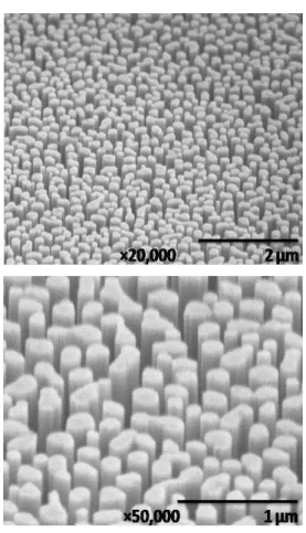
The shape and morphology of the GaN nanorods were observed using field emission scanning electron microscopy (FESEM). The side view image of GaN na-norods fabricated using top-down approach taken at different magnification (×20,000 and × 50,000) is shown in Fig. 2a, b. From the side-view secondary elec-tron image of the GaN nanorods cluster, the diameters of the nanorods on the sapphire substrate were about 100 to 250 nm. High vertical alignment of these nano-rods is also clear from secondary electron images.
3.2 Cathodoluminescence Studies
Cathodoluminescence (CL) measurements were also performed in order to investigate the light emission
Fig. 2 – FESEM image of GaN nanorods at two different magnifications (×20,000 and × 50,000)
Fig. 3 – CL spectrum of GaN nanorods at room temperature from mapped region showing two peaks which corresponds to band-edge luminescence (at 3.4 eV) and yellow band lumines-cence (centred about 2.3 eV)
properties of GaN nanorods. The CL measurements reported here were performed at room temperature using standard CL measurement set-up with accelerat-ing voltage of 5 kV and electron beam current of 20 A. Fig. 3 shows the CL spectrum of GaN nanorods from the mapped region.
CHARACTERIZATION OF GANNANORODS FABRICATED… J.NANO-ELECTRON.PHYS. 5, 02001 (2013)
02001-3 Fig. 4 – (a) FESEM image and (b) corresponding panchro-matic CL image of GaN nanorods
nanostructures fabricated from down-top approach [18-19]. The existence of YL indicates that there is a deep level located at about 2.3 eV below conduction band edge and recombination of conduction electrons through this deep level can give yellow emission
A plan-view integrated panchromatic CL image from GaN nanorods acquired with an accelerating volt-age of 5 kV and electron beam current of 20 A is
shown in Fig. 4a, b. Fig. 4a shows the FESEM image of GaN nanorods and Fig. 4b shows the corresponding panchromatic CL image. It is clear that CL intensity is not uniform and shows strong contrast between dark and bright regions. The bright spots in the image rep-resent high CL emission intensity while dark spots represent low emission intensity. The non-uniform CL emission is associated with the presence of extended crystalline defects such as dislocations which can act as the radiative centers. However, comparison between monochromatic CL imaging at 364 nm and 550 nm can give more information about these defects which is a matter of future investigation.
4. CONCLUSIONS
A different route for the fabrication of highly vertical-ly aligned GaN nanorods on c-plane sapphire is reported in this study. We fabricated GaN nanorods using a top-down approach by nanomasking and reactive ion etch-ing. The FESEM images indicated the GaN nanorods with diameter ranging between 100-250 nm were grown via top-down approach. FESEM images also indicated the highly vertical alignment of these nanorods. The CL analysis confirmed the formation and high optical prop-erties of GaN nanorods. These studies give us more un-derstanding about the fundamental properties of GaN nanomaterials and provide useful information in the application of GaN nanorods-based devices.
AKNOWLEDGEMENTS
Ashutosh Kumar is grateful to Council of Scientific and Industrial Research (CSIR) India for Senior Re-search Fellowship. The authors are thankful to Prof. Vikram Kumar for his valuable suggestion during this work. The authors (A.K. and R.S) are thankful to De-partment of Information Technology, Govt. of India for setting up Nanoscale Research Facility at IIT Delhi.
REFERENCES
1. Y. Xia, P. Yang, Y. Sun, Y. Bu, B. Mayers, B. Gates, Y. Fin, F. Kim, H. Yan, Adv. Mater. 15, 353 (2003). 2. J. Appenzeller, J. Knoch, T.M. Bjork, H. Riel, H. Schmid,
W. Riess, IEEE T. Electron Dev. 55, 2827 (2008).
3. X. Duan, Y. Huang, Y. Cui, J. Wang, C. M. Lieber, Nature
409, 66 (2001).
4. Y. Huang, X. Duan, Y. Cui, C.M. Lieber, Nano Lett. 2, 101 (2002).
5. S. Nakamura, T. Mukai, M. Senoh, Appl. Phys. Lett. 64, 1689 (1994).
6. J. Zhu, L. Wang, S. Zhang, H. Wang, D. Zhao, J. Zhu, Z. Liu, D. Jiang, H. Yang, J. Appl. Phys. 108, 074302 (2010).
7. C.J. Neufeld, C. Schaake, M. Grundmann, N.A. Fichtenbaum, S. Keller, U.K. Mishra, phys. status solidi c 4, 1605 (2007).
8. L. Nguyen, Gallium Nitride Nanowires, COSMOS (2012). 9. T. Fujii, Y. Gao, R. Sharma, E.L. Hu, S.P. DenBaars,
S. Nakamura, Appl. Phys. Lett. 84, 855 (2004).
10.C. Huh, K.-S. Lee, E.-J. Kang, S.-J. Park, J. Appl. Phys.
93, 9383 (2003).
11.H.W. Huang, J.T. Chu, C.C. Kao, T.H. Hseuh, T.C. Lu, H.C. Kuo, S.C. Wang, C.C. Yu, Nanotechnology 16, 1844 (2005).
12.R.S. Wagner, W.C. Ellis, Appl. Phys. Lett. 4, 89 (1964). 13.W. Han. S. Fan, Q. Li, Y. Hu, Science 277, 1287 (1997). 14.S. Li, A. Waag, J. Appl. Phys. 111, 071101 (2012).
15.V. Ramesh, A. Kikuchi, K. Kishino, M. Funato, Y. Kawakami, J. Appl. Phys. 107, 114303 (2010).
16.C.H. Chiu, T.C. Lu, H.W. Huang, C.F. Lai, C.C. Kao, J.T. Chu, C.C. Yu, H.C. Kuo, S.C. Wang, C.F. Lin, T.H. Hsueh, Nanotechnology 18, 445201 (2007).
17.H.W. Huang, J.T. Chu, T.H. Hsueh, M.C. Ou-Yang, H.C. Kuo, S.C. Wang, J. Vac. Sci. Technol. B 24, 1909 (2006).
18.S.O. Kucheyev, M. Toth, M.R. Phillips, J.S. Williams, C. Jagadish, Appl. Phys. Lett. 79, 2154 (2001).