Article
Printed in Brazil - ©2015 Sociedade Brasileira de Química0103 - 5053 $6.00+0.00A
*e-mail: [email protected]
Facile Microwave-Assisted Synthesis of Lanthanide Doped CaTiO
3Nanocrystals
Sandra C. Pereira,a Alberthmeiry T. Figueiredo,*,a Cristiano M. Barrado,a
Marcelo H. Stoppa,b Yashashchandra Dwivedi,c Maximo S. Lid and Elson Longoe
aDepartamento de Química, and bDepartamento de Matemática, Universidade Federal de Goiás - UFG, 75704-020 Catalão-GO, Brazil
cPhysics Department, National Institute of Technology Kurukshetra, Kurukshetra, Haryana 136119, India
dInstituto de Física, Universidade de São Paulo - USP, 13566-590 São Carlos-SP, Brazil
eINCTMN, Instituto de Química, Universidade Estadual de São Paulo - UNESP, 14801-970 Araraquara-SP, Brazil
This article discusses a simple approach for the microwave-assisted synthesis of good quality nanosized calcium titanate crystals doped with trivalent Tm and Yb lanthanide ions. The prepared nanoparticles had a microcube-like structure and a crystallite size of ca. 47 nm. The structure of the nanocrystals was analyzed by X-ray diffraction (XRD) and scanning electron microscopy (SEM), and their spectroscopic behavior was examined at a laser excitation wavelength of 350.7 nm. It
was found that doping CaTiO3 nanocrystals with Yb and Tm leads to about 250-fold brighter
photoluminescence (PL) emissions in the blue and near-infrared regions than that emitted by pure
CaTiO3 nanocrystals. The PL emission was correlated with the structural disorder.
Keywords: luminescence, spectroscopy, lanthanide elements, defect emissions, nanophosphors
Introduction
Calcium titanate (CaTiO3 or CT) is a versatile material
which is one of the major phases in synroc (synthetic rock) and widely used in the immobilization of high level nuclear waste. At low temperatures, CT shows ferroelectric or quantum paraelectric behavior and it is used in various electronic ceramic materials, ceramic industry, electroluminescent devices, and sensors, and is an efficient host for luminescence of lanthanide ions.1-6
High permittivity and low dielectric losses also make crystal CT a suitable candidate for microwave applications. Its photocatalytic activity has also been investigated and it demonstrates high performance in the degradation of organic dyes, pigments and microorganisms.7-9
The perovskite structured CT crystal was initially prepared by conventional solid-state reaction using a stoichiometric ratio of TiO2 and CaCO3 or CaO at
high temperatures. Various methods of synthesis have
been described for the synthesis of high quality CT nanocrystals.10-19 The crystal growth of CaTiO
3 hollow
crystals with different microstructures was investigated by Yang et al.20 Tyliszczak et al.21 synthesized CT
nanopowders via a mechanochemical method assisted by microwave irradiation from calcium oxide and titanium dioxide. In this context, microwave-assisted heating is a greener approach to synthesize materials in a shorter time (from a few minutes to several hours) while consuming less energy (hundreds of watts). Recent reports that discuss the microwave-assisted hydrothermal microwave (HTMW) synthesis of nanocrystalline titanate oxides,6, 13, 22-25 indicate
that the HTMW method is potentially a better way to synthesize crystalline CT powders at low temperatures and high heating rates.
In this perovskite, the substitution of the A site (Ca2+
ion) by trivalent ions (lanthanide (Ln) ions) leads to the formation of Ca2+ vacancies that affect the physical and
close to the coordinates of the “ideal red” color. The crystal structures in these cation-deficient perovskites are determined by the disposition of vacancies across the perovskite A-sites, and the tilting of the TiO6 octahedra.26
In this work, we used CT, one of the perovskite oxides, to prepare nanosized undoped and Thulium (Tm) and/or Ytterbium (Yb)-doped CT. The HTMW approach was selected to obtain powders under favorable conditions, i.e., low temperatures and a short reaction time (480 seconds). Detailed optical properties were evaluated using UV-Vis spectroscopy, and photoluminescence (PL) emission spectra of doped and undoped CT were employed to examine the structural order-disorder of the synthesized materials and the possible correlation between their structure and photoluminescence.
Experimental
Single crystalline phase samples of CaTiO3 (CT),
Ca0.99Tm0.005Yb0.005TiO3 (CT:Tm,Yb), Ca0.99Tm0.01TiO3
(CT:Tm), and Ca0.99Yb0.01TiO3 (CT:Yb) were synthesized by
reacting stoichiometric proportions of TiO(SO4) (Aldrich),
CaCl2.2H2O (Merck), Tm2O3 (Aldrich), Yb2O3 (Aldrich)
and KOH (Merck) using aqueous precipitation microwave. All chemicals are of purity better than 99.9% and used as obtained from vender.
Samples were prepared using following procedure. Firstly, TiO(SO4) was slowly added in 25 mL of deionized
water at 398 K under stirring, forming TiO(OH)2. In the
next step, stoichiometric amount of CaCl2.2H2O was added
in the prepared solution under rigorous stirring, resulting transparent solution, in which desired quantities of Tm3+
and/or Yb3+ were added. The salt of lanthanide elements
(Tm2O3 and Yb2O3) was prepared by dissolving require
amount of lanthanide oxide in concentrated HNO3. 50 mL
of a 6.0 mol L-1 KOH solution, which act as mineralize,
was further added to the prepared solution under constant stirring. This procedure promotes the co-precipitation of the amorphous titanium oxide (TiO(OH)2), as well as calcium
(Ca(OH)2) and Thulium and/or Ytterbium (Tm(OH)3 and/
or Yb(OH)3) hydroxides to form the reaction mixture. This
mixture was then transferred to a Teflon autoclave reaching 66% of its total volume allowing the maximum pressure efficiency. The autoclave was finally sealed and placed in the domestic HTMW system using 2.45 GHz microwave radiation with maximum power of 800 W. This mixture was heated at 413 K under nominal heating rate of 6.9 K s-1
(at 800 W) by direct interaction of water molecules with microwaves radiation and remained under constant pressure of 250 KPa for 480 seconds. After that, the autoclave was naturally cooled down to room temperature. The solid
product obtained was water washed until neutral pH, and then, dried at 353 K for 43,200 s. This procedure is similar to that used by Moreira et al.13 The Table 1 describes all
prepared samples.
The obtained powders were characterized by X-ray diffraction powder (XRD) in a Shimadzu XRD 6100 diffractometer, using a Cu Ka (k = 1.5406 Å) radiation in order to determine the structural evaluation. The data were collected from 10 to 80 degree in 2θ range with 0.5 degree
divergence slit and 0.3 mm receiving slit, using fixed-time mode, with 0.02 degree step size. Microstructural and morphological characterization was performed by field emission scanning electron microscopy (FE-SEM, Zeiss Supra 35), using 2 to 4 kV in different magnification. Excitation spectra were recorded on a Spex Fluorolog F2121 Spectrofluorimeter. The photoluminescence (PL) spectra were measured with a Thermal Jarrel-Ash Monospec 27 monochromator and a Hamamatsu R446 photomultiplier. The 350.7 nm exciting wavelength of a krypton ion laser (Coherent Innova) was used, with the laser’s nominal output power kept at 200 mW. All the measurements were taken at room temperature.
Results and Discussion
Figure 1 illustrates the XRD patterns of CT, CT:Tm,Yb, CT:Tm, and CT:Yb samples.
Table 1. Summary of prepared samples
Sample Ca / % Tm / % Yb / % Code
CaTiO3 100 0 0 CT
Ca0.99Tm0.005Yb0.005TiO3 99 0.5 0.5 CT:Tm,Yb
Ca0.99Tm0.01TiO3 99 1 0 CT:Tm
Ca0.99Yb0.01TiO3 99 0 1 CT:Yb
Figure 1. (A) XRD patterns of (a) CT, (b) CT:Tm,Yb, (c) CT:Tm, and (d)
The results indicated that the positions of the diffraction peaks and the relative diffraction intensities of the samples were well matched with the standard powder diffraction data (JCPDS card No. 22-0153), with space group Pnma 62 and lattice constants of 5.44, 7.643, and 5.381 Å, indicating crystallization of the typical single orthorhombic perovskite CaTiO3 phase, line (a) in Figure 1A.
Single crystalline CaTiO3 can be obtained at 413 K
and 25 kPa in 480 seconds, which is a comparatively lower temperature and shorter time than the conventional methods for synthesizing single phase CaTiO3.4 This finding
indicates that the HTMW method is efficient for obtaining single phase materials. In general, the microwave synthesis approach depends on certain experimental conditions of pressure, temperature and time, and facilitates the formation of phases in a relatively short time.
The average crystallite size (D) was calculated from the most intense peak in the XRD diffraction patterns (peak 121), using the Debye-Scherrer (equation 1):
k λ
D
B cosθ
× =
× (1)
where k is a constant of the shape factor, λ is the
characteristic X-ray wavelength of copper (1.54 Å), B is the FWHM in radians, and θ is the Bragg angle of (121) peak.27
The average crystallite sizes thus obtained were ca. 47 nm for CT, ca. 35 nm for CT:Tm,Yb, ca. 45.5 nm for CT:Tm, and ca. 39.6 nm for CT:Yb, confirming the nanodimensions of the synthesized crystalline materials.
The doped trivalent lanthanide ions were expected to occupy Ca2+ sites in the CaTiO
3 structure. To confirm this
assumption and understand the effect of lanthanide ion substitution, a comparison was made of the diffraction patterns of lanthanide doped samples (Figure 1). The calculated lattice parameters for these samples were 5.46, 7.642, and 5.339 Å (for CT); 5.459, 7.635, and 5.31 Å (for CT:Yb); 5.445; 7.628, and 5.30 Å (for CT:Tm); and 5.436, 7.624, and 5.297 Å (for CT:Tm,Yb). It is obvious that doping caused the diffraction peaks to shift towards higher angles, while only slightly modifying the lattice constant. The lattice parameters decreased only slightly in response to the substitution of Ca2+ ions (ionic radius ca. 114 pm)
for ions with similar ionic radius: Tm3+ (ca. 117 pm) and
Yb3+ ions (ca. 116 pm). The diffraction intensity of the
peaks was also found to decrease in the presence of doped ions, indicating a reduction in the number of CaTiO3
crystals.
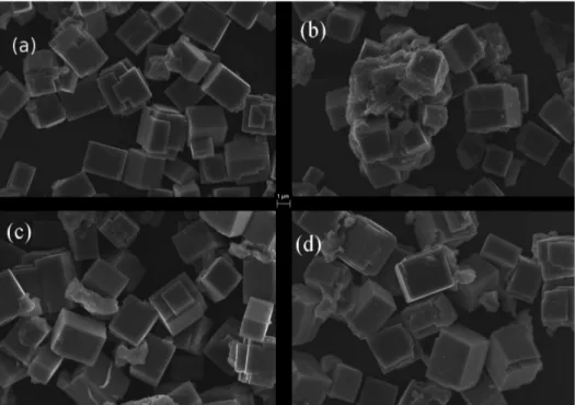
To examine the possible effect of Ln3+ on the crystal
morphology, field emission scanning electron microscopy (FE-SEM) images were recorded of the prepared samples (Figure 2).
These micrographs reveal the formation of a cube-like morphology with significant agglomeration. These microsize structures show sharp well-defined edges. Similar images are also reported in the literature.13,24 These cubes are great
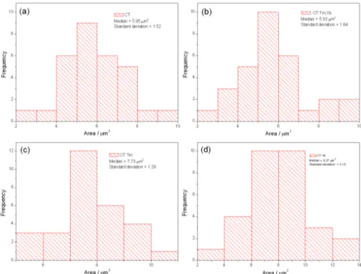
structures (ca. 2 mm), although they are formed by lots of nanocrystallites of the synthesized materials (ca. 40 nm). Histograms show the cube area and their frequency of occurrence to the obtained materials (Figure 3).
The Figure 4 proposes a mechanism to cubic morphology formation. The nanocubes growth an oriented aggregation according to the pseudocubic subunit. An Ostwald ripening process then leads to the disappearance of smaller nanocubes in the central area, forming microsize cubes.20
Lanthanide doping also affects the crystal morphology. Undoped CT shows a cubic morphology; however, although the reaction conditions are exactly the same, the micrograph of the dual doped CT:Tm,Yb sample shows cube-like structures and a region without well-defined morphology. Therefore, it can be stated that lanthanide ions likely contribute to create structural disorder in the system. The samples doped with Tm and Yb also show the typical cubic morphology, as well as a small portion with undefined morphology.
The PL spectra of CT, CT:Tm,Yb, CT:Tm, and CT:Yb were recorded in the range of 350-850 nm, at 350.7 nm excitation (Figure 5).
The PL spectrum of CT contains two broad asymmetrical luminescence bands centered at 475 and 761 nm, which are distributed in the range of 375-600 nm and 675-850 nm, respectively. Among these bands, the one centered at 761 nm is 16 times more intense than the band centered at 475 nm. The origin of these bands is ascribed to the
Figure 4. Illustration showing growth mechanisms to cubic morphology formation.
Figure 3. Histograms of area distribution to: (a) CT; (b) CT:Tm,Yb; (c) CT:Tm; and (d) CT:Yb.
Figure 5. PL spectra of CT, CT:Yb, CT:Tm and CT:Tm,Yb codoped
structural disorder of the CT structure.28 Moreira et al.13
found a correlation between PL emission and structural disorder in CT. These authors stated that CT powders synthesized by the HTMW method are crystalline with structural disorder, and that this disorder is responsible for the intermediate energy states within the band gap. These intermediate energy states are the ones mainly responsible for PL emission in CT.
HTMW processing also reportedly promotes an intrinsic disorder in crystalline structures by producing different angles in TiO6 octahedral, which are expected to be related
with luminescence. When a CT structure is doped with a trace amount of Yb ions, a very different band structure is observed, containing an asymmetrical band centered at 452 nm. In addition, three comparatively low intensity bands are also observed at 620, 729 and 821 nm. The Tm doped CT sample also showed three of the aforementioned four bands, i.e., at 451, 621 and 724 nm, but with a slight energy shift. In addition to these bands, two comparatively sharper peaks were also observed at ca. 467 and ca. 812 nm in the blue and near infrared regions. These emission peaks, which are ascribed to Tm3+, correspond to the 1G
4→3H6 and 3H
4→3H6 transitions, respectively.
The intensity of the blue emission appears weaker than that of the near-infrared emission. A comparison of an integrated area of the blue (467 nm) and NIR (812 nm) peaks indicates that the NIR peak is ca. 200-fold brighter than the blue band. In the presence of both the Ln3+ ions
(Tm and Yb), an entirely new feature becomes visible. The PL spectrum of CT:Tm,Yb contains two main bands, one corresponding to the blue region centered at ca. 447.5 nm and the other to the NIR band centered at ca. 763.3 nm. Since it is difficult to observe absorption peaks in the broad-host range, we monitored the excitation spectrum of the CT:Tm,Yb codoped sample at the 475 nm emission, which revealed at least three major asymmetric peaks at 371, 415 and 442 nm, and two comparatively weaker peaks at 363 and 424 nm (inset in Figure 5). It is expected that 350.7 nm laser photons absorb resonantly in the upper portion of the band centered at 371 nm. It has previously been reported that the occurrence of PL involves several steps, including the resonant excitation of O 2p electron states at a valence of up to Ti 3d states inside the forbidden band gap, which subsequently relaxes through a process of recombination near the conduction band and allows for 3d → 2p transition.12 It has also been stated that
the blue band attributed to electron-hole recombination centers is promoted by high energy defects, while NIR band is related to low energy defects.
There is ample experimental evidence, from diffraction studies,29-33 that titanate doped by trivalent lanthanide
present vacancies do indeed accumulate onto alternate A-site planes, that is there is a layered ordering involving the alternation of cation-rich and cation-poor planes. The vacancies produce structural defects into CT structure. So, we believe our dual doped CT sample contains more structural defects than the undoped CT sample. The introduction of Tm3+ and Yb3+ in the CT matrix
promotes distortions of the crystal lattice in response to the substitution of Tm3+ and Yb3+ ions in the A-site,
which give rise to new intermediate levels within the band gap due to the presence of oxygen vacancies.28,34,35
Charge compensation occurs through the formation of intrinsic defects, such as calcium and/or oxygen vacancies.36
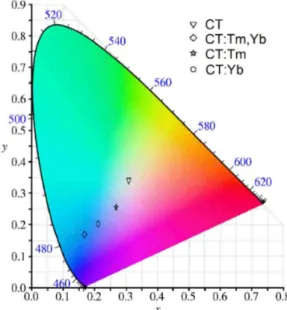
In order to compare among PL spectra of CT and doped CT samples, we used a colour-difference formula designed to give a quantitative value of the perceived colour difference among PL spectra of samples in specific experimental conditions.37,38 This procedure was used to
adjust the PL spectra in a mixture of three primary colors, each with fixed chromaticity, but with adjustable brightness. The Figure 6 shows the CIE (Commission Internationale de l’Eclairage) diagram for all of the CT and doped CT samples. The CIE chromaticity coordinates [x-axis, y-axis] for the samples are [x = 0.3087, y = 0.3413] to CT, [x = 0.2122, y = 0.2024] to CT:Yb, [x = 0.2686, y = 0.2550] to CT:Tm, and [x = 0.1682, y = 0.1692] CT:Tm,Yb.
It is interesting to note that the increasing amount of defects in the presence of lanthanide doping of CT:Tm,Yb augmented the band intensity in the blue region by about 250-fold compared to that of the CT sample. So, the doped
CT samples present different emission to undoped CT. The doping foreign elements into a semiconductor with wide band gap to create a new optical absorption edge is known to be one of the primary strategies for developing materials with optical-driven properties. However, the role of the rare earth in the perovskite structure is not really clear and is still being discussed. Further experimentation is needed to explore the cause of the defects in CT in the presence of Tm and Yb ions.
Conclusions
High quality cube-shaped CaTiO3 nanocrystals with a
size of ca. 47 nm were synthesized using an easy microwave heating method coupled with a co-precipitation method. These nanocrystals were then doped with Tm, Yb and with the two ions and were analyzed in depth based on XRD, SEM, excitation and PL spectra. The microwave-assisted synthesis of Ln3+-doped CaTiO
3 offers the advantage of rapid
crystallization. It was observed that CaTiO3 nanocrystals
doped with Yb and Tm emitted photoluminescence in the blue and near-infrared regions that was ca. 250 times brighter than that of pure CaTiO3 nanocrystals. The
structural disorder and photoluminescence emission were found to be correlated.
Acknowledgements
The authors thank the Brazilian research financing institutions FAPEG, CAPES and CNPq for their funding of this work. This work was supported by INCTMN/CNPq, Brazil.
References
1. Suvorov, D.; Valant, M.; Jancar, B.; Skapin, S. D.; Acta Chim. Slov.2001, 48, 87.
2. Lemanov, V. V.; Sotnikov, A. V.; Smirnova, E. P.; Weihnacht, M.; Kunze, R.; Solid State Commun.1999, 110, 611.
3. Fu, Q.; Li, J. L.; He, T.; Yang, G. W.; J. Appl. Phys.2013, 113,
104303.
4. Wong, Y. J.; Hassan, J.; Hashim, M.; J. Alloy. Compd.2013, 571, 138.
5. Tsuchiya, T.; Nakajima, T.; Shinoda, K.; Mater. Lett.2013, 108,
176.
6. Dwivedi, Y.; Zilio, S. C.; J. Nanosci. Nanotechnol.2014, 14,
1578.
7. Lee, S. W.; Lozano-Sanchez, L. M.; Rodriguez-Gonzalez, V.;
J. Hazard. Mater.2013, 263, 20.
8. Kimijima, T.; Kanie, K.; Nakaya, M.; Muramatsu, A.;
CrystEngComm2014, 16, 5591.
9. Huo, Y. S.; Yang, H.; Xian, T.; Jiang, J. L.; Wei, Z. Q.; Li, R. S.; Feng, W. J.; J. Sol-Gel Sci. Technol.2014, 71, 254.
10. Zhao, H. Y.; Duan, Y. W.; Sun, X.; New J. Chem.2013, 37, 986. 11. Shivaram, M.; Krishna, R. H.; Nagabhushana, H.; Sharma,
S. C.; Nagabhushana, B. M.; Ravikumar, B. S.; Dhananjaya, N.; Shivakumara, C.; Rao, J. L.; Chakradhar, R. P. S.; Mater. Res. Bull.2013, 48, 1490.
12. Ovenstone, J.; Romani, J. O.; Davies, D.; Misture, S.; Silver, L. In Developments in Strategic Materials; Lin, H.; Koumoto, K.; Kriven, W.; Garcia, E.; Reimanis, I.; Norton, D.; Ohji, T.; Wereszczak, A., eds.; J. Wiley & Sons. Inc.: New Jersey, 2009, p. 285.
13. Moreira, M. L.; Paris, E. C.; do Nascimento, G. S.; Longo, V. M.; Sambrano, J. R.; Mastelaro, V. R.; Bernardi, M. I. B.; Andres, J.; Varela, J. A.; Longo, E.; Acta Mater. 2009, 57, 5174. 14. Cavalcante, L. S.; Marques, V. S.; Sczancoski, J. C.; Escote,
M. T.; Joya, M. R.; Varela, J. A.; Santos, M.; Pizani, P. S.; Longo, E.; Chem. Eng. J.2008, 143, 299.
15. Yin, S. Y.; Chen, D. H.; Tang, W. J.; Peng, Y. H.; Mater. Sci. Eng. B-ADV.2007, 136, 193.
16. Patil, B. M.; Srinivasa, R. S.; Dharwadkar, S. R.; Bull. Mater. Sci.2007, 30, 225.
17. de Figueiredo, A. T.; de Lazaro, S.; Longo, E.; Paris, E. C.; Varela, J. A.; Joya, M. R.; Pizani, P. S.; Chem. Mater.2006, 18, 2904.
18. Dong, W. J.; Li, X. Y.; Yu, J.; Guo, W. C.; Li, B. J.; Tan, L.; Li, C. R.; Shi, J. J.; Wang, G.; Mater. Lett.2012, 67, 131. 19. Dong, W. J.; Li, B. J.; Li, Y.; Wang, X. B.; An, L. N.; Li, C. R.;
Chen, B. Y.; Wang, G.; Shi, Z.; J. Phys. Chem. C2011, 115, 3918.
20. Yang, X. F.; Fu, J. X.; Jin, C. J.; Chen, J. A.; Liang, C. L.; Wu, M. M.; Zhou, W. Z.; J. Am. Chem. Soc.2010, 132, 14279.
21. Tyliszczak, B.; Gaca, K. Z.; Sobczak-Kupiec, A.; Dulian, P.;
J. Eur. Ceram. Soc.2014, 34, 2259.
22. Souza, A. E.; Santos, G. T. A.; Silva, R. A.; Moreira, M. L.; Volanti, D. P.; Paris, E. C.; Teixeira, S. R.; Longo, E.; Int. J. Appl. Ceram. Technol.2012, 9, 186.
23. Souza, A. E.; Silva, R. A.; Santos, G. T. A.; Moreira, M. L.; Volanti, D. P.; Teixeira, S. R.; Longo, E.; Chem. Phys. Lett. 2010, 488, 54.
24. Mazzo, T. M.; Moreira, M. L.; Pinatti, I. M.; Picon, F. C.; Leite, E. R.; Rosa, I. L. V.; Varela, J. A.; Perazolli, L. A.; Longo, E.;
Opt. Mater.2010, 32, 990.
25. Chen, R.; Chen, D. H.; J. Alloys Compd.2009, 476, 671.
26. Pirc, R.; Blinc, R.; Phys. Rev. B: Condens. Mater. Phys.2004,
70, 134107.
27. Langford, J. I.; Wilson, A. J. C.; J. Appl. Crystallogr.1978, 11, 102.
28. de Figueiredo, A. T.; Longo, V. M.; da Silva, R. O.; Mastelaro, V. R.; Mesquita, A.; Franco, R. W. A.; Varela, J. A.; Longo, E.;
29. King, G.; Woodward, P. M.; J. Mater. Chem.2010, 20, 5785. 30. Zhang, Z. M.; Lumpkin, G. R.; Howard, C. J.; Knight, K. S.;
Whittle, K. R.; Osaka, K.; J. Solid State Chem.2007, 180, 1083. 31. Howard, C. J.; Zhang, Z. M.; J. Phys. Condens. Matter2003,
15, 4543.
32. Yashima, M.; Ali, R.; Yoshioka, H.; Solid State Ionics2000, 128, 105.
33. Abe, M.; Uchino, K.; Mater. Res. Bull.1974, 9, 147.
34. Dawson, J. A.; Li, X.; Freeman, C. L.; Harding, J. H.; Sinclair, D. C.; J. Mater. Chem. C2013, 1, 1574.
35. Zamkova, N. G.; Zinenko, V. I.; Shinkorenko, A. S.;
Ferroelectrics2012, 426, 132.
36. Dwivedi, Y.; Bahadur, A.; Rai, S. B.; J. Appl. Phys. 2011, 110, 43103.
37. de Orbe-Paya, I.; Erenas, M. M.; Capitan-Vallvey, L. F.; Sens. Actuators, B2007, 127, 586.
38. Erenas, M. M.; Cantrell, K.; Ballesta-Claver, J.; de Orbe-Paya, I.; Capitan-Vallvey, L. F.; Sens. Actuators, B2012, 174, 10.
Submitted: May 29, 2015
Published online: September 9, 2015
![Optical Properties of MEH-PPV and MEH-PPV/ [6,6]-Phenyl C61-butyric Acid 3-ethylthiophene Ester Thin Films](data:image/gif;base64,R0lGODlhAQABAIAAAP///wAAACH5BAEAAAAALAAAAAABAAEAAAICRAEAOw==)