Juliano Fujioka Mologni* Engineering Simulation and Scientiic Software
São Paulo – Brazil [email protected]
Marco Antonio Robert Alves State University of Campinas Campinas – Brazil [email protected]
Filipe Braumgratz State University of Campinas Campinas – Brazil [email protected]
Edson Fonseca State University of Campinas Campinas – Brazil [email protected]
Cesareo L. R. Siqueira Engineering Simulation and Scientiic Software
São Paulo – Brazil [email protected]
Edmundo Silva Braga State University of Campinas Campinas – Brazil [email protected]
* author for correspondence
Optimizing the e-beam proile
of a single carbon nanotube
ield emission device for electric
propulsion systems
Abstract: Preliminary studies on ield emission (FE) arrays comprised of carbon nanotubes (CNT) as an electron source for electric propulsion system show remarkably promising results. Design parameters for a carbon nanotube (CNT) ield-emission device operating on triode coniguration were numerically simulated and optimized in order to enhance the e-beam focusing quality. An additional focus gate (FG) was integrated to the device to control the proile of the emitted e-beam. An axisymmetric inite element model was developed to calculate the electric ield distribution on the vacuum region and a modiied Fowler-Nordheim (FN) equation was used to evaluate the current density emission and the effective emitter area. Afterward, a FE simulation was employed in order to calculate the trajectory of the emitted electrons and deine the electron-optical properties of the e-beam. The integration of the FG was fully investigated via computational intelligence techniques. The best performance device according to our simulations presents a collimated e-beam proile that suits well for ield emission displays, magnetic ield detection and electron microscopy. The automated computational design tool presented in this study strongly beneits the robust design of integrated electron-optical systems for vacuum ield emission applications, including electrodynamic tethering and electric propulsion systems.
Keywords: Electric propulsion, Carbon nanotube, Finite element analysis.
INTRODUCTION
Field Emission (FE) cathodes consisted of Carbon Nanotubes (CNT) applied to electric propulsion systems are being developed due to their superiority over thermionic cathodes regarding power, mass and expellant consumption (Oakwa et al., 2007 and Marreses-Reading, 2002). The initial studies demonstrating the outstanding performance of CNT as a cold electron ield emitter were irstly reported in 1995 by (Chernozatonskii et al., 1995). The highly stable crystalline structures along with high aspect ratios are the CNT’s main characteristics responsible for high current density emitted and great ield enhancement factors (Young, 1958). Regarding ield emission phenomenon, CNTs are either arranged in a form of a ilm with a variety of densities and patterns, or projected as an individual CNT electron source. The irst ield emission experiment of a single nanotube as an electron source was reported by Rinzler et al. (1995) whereas the emission results followed an approximate Fowler-Nordheim (FN) behavior. Further studies on single CNTs ield emitter were conducted on numerous
areas, including theoretical analysis (Seidl et al., 2000 and De Heer et al., 1995), high vacuum experiments (Choi et al., 2004) and numerical simulation (Chen et al., 2007).
Understanding the fundamental CNT emission properties is necessary to design ield emission systems with optimal performance. A previous work by Edgecomb and Valdre (2001) reported the electrostatic properties behavior of single CNT system as a function of the emitter aspect ratio. Besides electric ield distribution and current density, the e-beam proile is an important characteristic and must be considered especially in applications involving ield emission displays and electron microscopy. A highly focus e-beam shape can considerably improve the performance of ield emission displays by improving their brightness and avoiding cross-talks between adjacent phosphorous cells. According to Itoh (1998) and Lei (2004), a good focusing also enhances the resolution of critical-dimension scanning electron microscopy (CDSEM) and boosts the performance of electric propulsion systems. This paper reports a numerical investigation of e-beam shape for an individual CNT ield emitter operating on a triode coniguration system with an integrated FG. The effects of physical design parameters and electrode voltage on the emitted e-beam shape are herein presented. Furthermore,
an automated computational tool was developed to numerically simulate several physical models using the inite element method (FEM).
THE FINITE ELEMENT MODEL
The ideal computational model is the one that provides the most accurate results with less complexity. Since we intend to perform simulations on a variety of scenarios, the computational process is critical and must be taken in consideration. Figure 1 shows the coniguration of the device detailing the geometric variables considered on our simulations.
the electrical loads used as input variables. To investigate the effects of these variables on emitted e-beam proile is the main objective of this paper.
The positive voltage applied to the extraction gate generates an electric ield that accelerates the electrons on the CNT surface toward the vacuum region via quantum tunneling. The electrons are then accelerated in the direction of the anode and their trajectories are inluenced by the electric ield generated by the FG.
The coaxial FG act as an electrostatic lens and control the e-beam inal proile, with little participation on the emitted current density (the FG slightly affects the current emitted; some studies will be presented later on in this paper). For that reason, the aperture of the FG is always larger than the extraction gate.
Considering the nature of the geometries and loads presented in the system, one can use symmetry techniques in order to simplify the model and, therefore, reduce computational effort. It is possible to observe the rotational symmetry around the longitudinal axis of the CNT nanostructure. Mathematical calculations may be applied only on one half of the cross-sectional view and the results may be rotationally expanded. Figure 2 details the inite element model with gates rotationally expanded 180o and
the CNT structure along with the cathode rotated 360o.
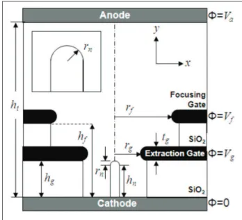
Figure 1: Cross-sectional schematic plot of the individual CNT FE system with an integrated FG. The inset image details the CNT tip radius.
Some physical parameters such as the CNT tip radius (rn) and height (hn), the extraction gate radius (rg) and height (hg), the FG radius (rf), the gate thickness (tg) and the distance between the cathode and anode (ht) are assumed as constants in this study. Conventionally, the cathode voltage is grounded and is set to zero. The values of the constant parameters are shown on Tab. 1.
Table 1: Constant parameters
Parameter rn hn rg hg rf tg ht Va
Value 5 40 30 50 60 20 4 300
Unit nm nm nm nm nm nm mm V
The FG height (hf) is the only physical parameter considered in this study that inluences the e-beam proile. The FG voltage (Vf) and the extraction gate voltage (Vg) are
Figure 2: The axisymmetric inite element model 3D. The SiO2 insulator layers and the vacuum mesh are omitted in this plot for a better visualization of the system. The cathode and CNT nanostructure are represented by white elements. The dark gray elements represent the FG and the light gray, the extraction gate.
NUMERICAL ANALYSIS
∇2
Φ = ∂
2
Φ ∂x2 +
∂2
Φ
∂y2 =0 (1)
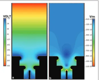
The electric ield distribution is then calculated by numerically differentiating the potential distribution with respect to x and y Cartesian coordinates. Numerical and graphical results for each step of our mathematical procedure are shown on Figures 3 to 5 using the following parameters: Vf=-10V; Vg=150V; and hf=100nm.
Figure 3 shows the resulting electrical potential and electric ield distribution. The maximum electric ield value is found at the CNT tip surface and is responsible for the ield emission phenomena. As observed in Fig. 4, the electrical potential varies linearly at regions positioned distantly from the CNT structure. As a result, the electrons situated in this region low linearly toward the anode surface. The developed tracing algorithm considers only two forces acting over the electron trajectories in this area: the electric ield generated by the anode voltage and the electron inertial forces previously acquired by the extraction gate and FG electric ields.
CNT surface area. A computer algorithm code was already developed for this purpose and presented by Fransen, Rooy and Kruit (1999).
Itip = J(E)ds
CNT
∫∫
(3)Figure 5 shows the distribution of current density emission at the CNT surface. It is possible to notice that only a small effective area of the CNT tip is responsible for the emitted current. To predict the emitted electrons trajectories, we need to set the initial coordinates on the CNT surface. All nodes located on the effective emitter surface area with non-zero current density values are selected to be the initial coordinates of the electron trajectories.
Figure 3: (a) Cross-sectional view showing the voltage contour plots on vacuum region; (b) Electric ield distribution.
Using the electrostatic analysis results, one can determine the emission current density from the CNT emitter using the following FN equation (Liao et al., 2007 and Niemman
et al., 2007), where (J) is the current density emitter ; (A) = 1.54 × 10⁻⁶; (B) is -6.83 × 10⁷; (φ) is the work function
of the emitter in eV; (E) is the electric ield in V/m, (t) can be approximated to 1; v(y) = -0.75y2 – 0.26y + 1.01; and
y = 3.79 × 10⁻⁴ (E0.5 / φ).
J(E)= AE
2
φt2(y)
⎛ ⎝
⎜ ⎞
⎠
⎟exp −Bφ
3/ 2v(y)
E
⎛ ⎝
⎜ ⎞
⎠
⎟ (2)
The total emitted current (Itip) is then evaluated via surface
integral using the electric ields values over the entire
Figure 4: Spatial electric potential distribution.
Figure 5: Surface plot showing the spatial emission current density on the surface of the CNT emitter. As expect-ed, the maximum current density is found on coordi-nates (x,y)=(0,0).
f(t,y)=m a
{ }
={ }
F =q E(
{ }
+{ }
v ×{ }
B)
(4)Where the mass of electron (m) is 9.109e-31 kg, charge of electron (q) is –1.602e-19 C, {E} is the electric field vector, {B} is the magnetic field vector, {F} is the Lorentz force vector, {a} is the acceleration vector and {v} is the velocity vector. The time integration is evaluated using the 4th order Runge-Kutta (RK)
numerical method:
y´= f(t,y)0;y(t0)= y0 (5)
Where yn+1 is the RK4 approximation of y(tn+1) and:
yn+1=yn+α
6
(
k1+2k2+2k3+k4)
;tn+1=tn+ αk1= f t
(
n,yn)
;k2 = f tn+α2,yn+
α
2k1
⎛ ⎝
⎜ ⎞
⎠
⎟ (6)
k3= f tn+α
2,yn+
α
2k2
⎛ ⎝
⎜ ⎞
⎠
⎟; k4= f t
(
n+ α,yn+ αk3)
where k is the RK function and is α constant.
When located at the vacuum mesh, the electron tracing follows from element to element. The exit point of the current element becomes the entry point of a new element. The exit location and velocity for an element is obtained by integrating the equations of motion using the RK method described above. The particle tracing algorithm exploits the following assumptions:
1. No relativistic effects (electron velocity is much smaller than speed of light and the electron mass is constant).
2. The electric ield within an element is constant. These simpliications reduce the computational time of the tracing algorithm.
The effectiveness of focusing is measured by the current-weighted beam radius at the anode surface. It represents the e-beam spot size (rb) and is calculated by:
rb=2× 0 J(r)r2πr dr
∞
∫
J(r)2πr dr
0
∞
∫
(7)Where J(r) is the electron current density at the anode as a function of the distance from the azimuthal symmetry axis and r is the tip radius.
A computational batch process algorithm was developed and the mathematical procedures described above were performed several times with multiple input variables. The analysis output the following parameters: e-beam
spot size on the anode, visual e-beam proile, current density and electric ield distribution.
RESULTS AND DISCUSSION
The Response Surface Modeling (RSM) technique was used to demonstrate the dependence of each input variable (hf, vf
and vg) on the output result (EFmax, rb). The computational automated code presented by Mologni et al. (2006) allows the generation of RSM on the ly, interpolating a matrix of discrete results using polynomial it functions.
Since the additional FG was integrated to the structure to work as a focus lens only, it’s reasonable to primarily investigate the inluence of vf and hf on the current density. Based on the FN Eq. (2), one can conclude that the emitted current density is proportional to the maximum electric ield value (EFmax) located at the tip of the emitter structure. A simulation to obtain RSM of the EFmax as a function of Vf and hf was then performed.
A linear relationship between the EFmax and Vf for any given value of hf is observed on Fig. 6. This is expected since all other electrical loads considered in the system are kept constant during this analysis and the space charge effect is disregarded. It is also possible to note an exponential dependence of the EFmax as a function of hf. When the FG is positioned far from the extraction gate (hf >> hg), the inluence of Vf on EFmax tends to saturate. This is explained by the high anode voltage and the great distance between the FG and the CNT emitter. If the FG is satisfactorily positioned far from the extraction gate so parallel electric potential lines between the gates can be observed, the saturation effect is achieved. The behavior of the variables presented above are only valid when we assume that Vf
is applied for focusing purposes only and is very small compared to the anode and extraction gate voltages.
For our study, the e-beam proiles were classiied into four broadens categories:
1. No focusing – No bias is applied to the focus gate (Fig. 7a).
2. Under-focused – Vf is highly positive and attracts the electrons on the vacuum region(Fig. 7b).
3. Over-focused – Vf is negative enough to repel the electrons and at least one trajectory cross the central symmetry axis before reaching the anode (Fig. 7c).
4. Focused – The smallest rb possible provided by the best combination of hf and Vf (Fig. 7d).
rb increases. High values of rb are also observed when vf
is extremely positive and the e-beam proile tends to be under-focused.
Figure 7: E-beam proile classiication.
The values of trajectory, velocity and time are calculated for each emitted electron using the Lorentz Eq. (4). When a bias is applied to the FG, the electric ield generated by vf
irst decreases the electron velocity to adjust the trajectory and, then, accelerates the electron toward the anode. The region near the FG is considered to be a turbulent electric ield region due to the variant FG electric potential. The combination of the FG and EG electric ields in this area force the electron to change its trajectory in a signiicant way. When the electron leaves the turbulent electric ield region, the dependence of the electron velocity relies only on the anode electric ield. Besides the boost on the performance of ield emission displays and CDSEM, the collimation effect combined with high velocity electrons also enhances the accuracy of FE systems when they are applied to detect the presence and the strength of magnetic ields (Fig. 8).
Figure 9 shows the resulting e-beam spot size for a set of FG height and voltage values. The best e-beam weighted radius that can be achieved in this system is 15.43 nm. If necessary, additional focus gates may be integrated to the system to further increase the focusing properties. The narrowest e-beam radius can be obtained for any hf
by applying a different vf. At highly negative values of
vf, the e-beam becomes over-focused and the value of
Figure 8: Electron velocity. Parameters used for this analysis:
vf=-20 V (for the focused electron trajectory case) and hf=90 nm.
Figure 9: Effects of FG height and voltage on e-beam weighted radius on the anode.
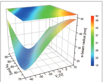
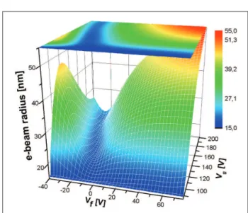
T
he e-beam proile also shows a dependence on the gate electric ield strength. In order to understand the e-beam weighted radius behavior for different gates biases, a simulation considering hf constant was assumed and the results are presented in Fig. 10.Figure 10: 3D surface plot of the e-beam weighted radius as a function of the applied gate voltages. The focus gate height was set to 90 nm for this particular case.
over-focused trajectory. On the other hand, higher values of vf and vg results on large rb, but, in this case, the e-beam
is comprised of under-focused electron trajectories. To correct under-focused trajectories, higher values of vf (in magnitude) are required. It is also important to consider the increase in the effective emitter area (Fig. 5) as the vg
values raises, resulting on large e-beam proiles.
With the analysis described above, one can always modulate the biasing of the gates in order to achieve the desired e-beam weighted radius. The numerical procedure herein described may be applied to any FE system by changing the initial inite element model and carefully choosing the boundary conditions.
CONCLUSIONS
In summary, we have performed several simulations indicating the optimal FG physical and electrical parameters to achieve the best e-beam proile for a single CNT FE device regarding electric propulsion systems. An automated computational process was developed to assist the numerous simulations of diverse initial conditions. The algorithm and procedure presented in this paper can be used to simulate any geometry having at least one variable parameter. The inluence of the integrated FG on the current density was also analyzed. It was shown that the presence of the FG inluence the current density on the surface of the CNT emitter, especially when the FG is positioned near the extraction gate. Physical parameters of the system combined with a range of electrical loads produce a variety of e-beam proiles. The resulted proiles were determined for numerous geometric structures and the smallest e-beam spot size for a given system is achieved by using different combinations of biasing.
ACKNOWLEDGEMENT
The authors would like to acknowledge Coordenação de Aperfeiçoamento de Pessoal de Nível Superior (CAPES) and Fundação de Amparo à Pesquisa do Estado de São Paulo (FAPESP) for their support.
REFERENCES
Chen, P.Y., et al., 2007, “Optimal design of integrally gated CNT ield-emission devices using a genetic algorithm”, Nanotechnology, Vol. 18, 10p. doi: 10.1088/0957-4484/18/39/395203.
Chernozatonskii, L.A., et al., 1995, “Electron ield emission from nanoilament carbon ilms”, Chem Phys Lett, Vol. 233, pp. 63-68.
Choi, J.E., et al., 2004, “Carbon nanotube ield emitter arrays having an electron beam focusing structure”, Appl Phys Lett, Vol. 84, pp. 1022-1025.
De Heer, W.A., Châtelain, A., Ugarte, D., 1995, “A carbon nanotube ield-emission electron source”, Science, Vol. 270, pp.1179-1180.
Edgcombe, C.J., Valdre, U., 2001, “Microscopy and computational modeling to elucidate the enhancement factor for ield electron emitters”, J Microsc, Vol. 203, pp. 188-194.
Fransen, M.J., Rooy, T.L., Kruit, P., 1999, “Field emission energy distribution from individual carbon nanotube”, Appl Surf Sci, Vol. 146, pp. 312-327.
Itoh, J. Uemara S.K., Kanemaru S., 1998, “Three-dimensional vacuum magnetic sensor with a Si emitter tip”, J Vac Sci Technol B, Vol. 16, pp. 1233-1235.
Lei, W., Yang, G., Xie, M., 2004, “Study of the triode structure in a ield emission display element”, J Vac Sci Technol B, Vol. 24, pp. 962-964.
Liao, K.P., Hu, Y., Lin, T.L., 2007, “Simulation studies of self-focusing carbon nanotube ield emitter”, J Vac Sci Technol B, Vol. 25, pp. 84-86.
Marreses-Reading, C., et al., 2002, “Field emission array cathode material selection for compatibility with electric propulsion applications”, Nasa JPL Technical Report, No. 8523, 17p.
Niemman, D.L., et al., 2007, “Effects of cathode structure on the ield emission properties of individual multi-walled carbon nanotube emitters”, Nanotechnology, Vol. 18. doi: 10.1088/0957-4484/18/48/485702.
Okawa, Y., et al., 2007, “An experimental study on carbon nanotube cathodes for electrodynamic tether propulsion”, Acta Astronautica, Vol. 61, pp. 989-994.
Rinzler, A.G., et al., 1995, “Unraveling nanotubes: ield emission from an atomic wire”, Science, Vol. 269, pp.1550-1553.