Comprehensive Study of Growth Mechanism and Properties of Low Zn Content Cd
1–xZn
xS
Thin Films by Chemical Bath
Carlos Aníbal Rodríguez a*, Myrna Guadalupe Sandoval-Paz b, Renato Saavedrab,c, Cuauhtémoc
Trejo-Cruz d, Francisco De la Carrera b, Luis E. Aragone, Martín Sirena e, Marie-Paule Delplanckef,
Claudia Carrasco g
Received: October 30, 2015; Revised: August 18, 2016; Accepted: September 04, 2016
Cd1–xZnxS thin ilms have been studied extensively as window layers for solar cell applications. However, a mismatch between the Cd1–xZnxS and copper–indium–gallium–selenide absorber layers
increases with Zn ilm concentration, which reduces the device eiciency. In this work, Cd1–xZnxS
thin ilms with low Zn concentrations were analyzed. The efect of the addition of diferent molar Zn concentrations to the reaction mixture on the growth mechanism of Cd1–xZnxS thin ilms and the
inluence of these mechanisms on structural, optical and morphological properties of the ilms has been studied. Cd1–xZnxS thin ilms were synthesized by chemical bath deposition using an ammonia-free
alkaline solution. Microstructural analysis by X-ray difraction showed that all deposited ilms grew with hexagonal structure and crystallite sizes decreased as the Zn concentration in the ilm increased. Optical measurements indicated a high optical transmission between 75% and 90% for wavelengths above the absorption edge. Band gap value increased from 2.48 eV to 2.62 eV, and the refractive index values for Cd1–xZnxS thin ilms decreased as the Zn increased. These changes in ilms and properties
are related to a modiication in growth mechanism of the Cd1–xZnxS thin ilms, with the inluence of
Zn(OH)2 formation being more important as Zn in solution increases.
Keywords: Cd1–xZnxS; chemical bath deposition; optical properties; structural properties.
* e-mail: [email protected]
1. Introduction
Cd1–xZnxS thin ilms have attracted attention for a long time, since their energy band gap can be tuned and their lattice parameters can be modiied with variation in Zn concentration1-3. Replacement of CdS with higher energy
gap ternary Cd1–xZnxS in thin-ilm solar cells, based on CdTe
or copper–indium–gallium–selenide (CIGS) absorbers, is expected to decrease window absorption losses and result in an improved solar cell performance4,5. Several studies
have focused on the deposition of Cd1–xZnxS thin ilms
with diferent Zn contents6-8, but the Zn content that has
been studied thus far has always been larger than 5 at.%. Therefore, the range of very low Zn contents below 5%
has not been studied to date. An investigation of this small range of compositions increased in importance because, as reported by Burton et al.9 and Reddy et al.10, a higher Zn
concentration leads to a large lattice mismatch with CIGS-absorber material and a higher resistivity material, which increases the series resistance of thin-ilm solar cell devices. The lattice mismatch between window and absorbent layers is important to considerer in heterojunction solar cell device manufacture. Defects in junctions introduce energy levels in the band structure, which act as recombination sites and reduce the conversion eiciency of the devices11. A
near-perfect lattice match is obtained between the absorber CIGS-(1 1 2) tetragonal plane and the window CdS-(1 0 0) hexagonal phase plane. Accordingly, the Zn concentration in Cd1–xZnxS ilms should be kept as low as possible, whereas
a Multidisciplinary Research Institute in Science and Technology, Ineergias, University of La Serena,
Benavente 980, La Serena, Chile
b Department of Physics, Faculty of Physical and Mathematical Sciences, University of Concepción,
Esteban Iturra s/n, Casilla 160-C, Concepción, Chile
c Center for Optics and Photonics, Universidad de Concepción, Casilla 4016, Concepción, Chile
d Department of Physics, Faculty of Sciences, University of Bíobio, Avenida Collao 1202 casilla 5C,
Concepción 4051381, Chile
e Centro Atómico Bariloche & Instituto Balseiro, CNEA & Univ. Nac. de Cuyo, Av. Bustillo 9500, 8400
Bariloche, Rio Negro, Argentina
f 4MAT, Université Libre de Bruxelles, Avenue Roosevelt 50, CP 165/63, Brussels 1050, Belgium
g Department of Materials Engineering, Faculty of Engineering, University of Concepción, Edmundo
the optical transmission and band gap should be increased as much as possible.
Cd1–xZnxS thin ilms were deposited by chemical bath deposition (CBD), which is a very simple, inexpensive and efective technique for the deposition of various semiconductor materials. It is well known that the initial reaction solution conditions in CBD determine the properties of the obtained ilms; however, few studies have focused on the growth mechanisms and subsequent ilm properties. Hodes et al.3 concluded that the thickness and crystal size
of thin ilms produced by CBD are strongly dependent on growth mechanisms. Therefore, it is also possible to relate the optical ilm properties to the growth mechanism. For example, Rodríguez et al. demonstrated that the growth mechanism afects the morphological properties and chemical composition of ZnS thin ilms grown by CBD from a non-toxic alkaline solution12, which can afect optical properties.
Another important factor in the synthesis of Cd1–xZnxS thin
ilms by CBD is the reaction solution composition. Most reports found in literature use ammonia as complexing agent in the aqueous synthesis of semiconductor thin ilms1,2,6,7. However, this
is a highly volatile, toxic and harmful material8, and industrial
production would produce serious environmental and health problems. Considering the large amount of waste derived from the deposition process, the use of non-toxic precursors in ilm synthesis reduces the current environmental crisis.
We present on a detailed study of the growth mechanisms involved in CBD of the Cd1–xZnxS ternary compound to
understand the synthesis of Cd1–xZnxS thin ilms better. The
efects of very low Zn concentration (less than 5 at.%) on chemical, structural, optical and morphological properties are analyzed and interpreted in terms of growth mechanisms.
2. Experimental Procedure
Cd1–xZnxS thin ilms with low Zn content were deposited on glass slide substrates using an ammonia-free CBD process, which has been used previously to deposit CdS thin ilms13,14
and aqueous solutions of 0.05 M CdCl2, 0.5 M C6H5O7Na3
(sodium citrate, Sigma-Aldrich), 0.5 M KOH (J.T. Baker), pH 10 borate bufer solution (Winkler), and 0.5 M CS(NH2)2
(thiourea, Sigma-Aldrich). Five types of Cd1–xZnxSilms were
studied, where the Zn concentration in the reaction mixture was increased from 0 (used as reference) to 1.5×10⁻³ M by
adding Zn(CH3COO)2 (Sigma-Aldrich), while maintaining all
other reactant concentrations unchanged. The molar ratio, r = [Zn]/[Zn+Cd], in each reaction solution was 0, 0.05, 0.07, 0.09, and 0.13. All studied thin ilms were deposited at a solution temperature of 70°C and pH 11.5. Four samples were deposited for each condition by placing four substrates in the reaction beaker and then removing them from solution after 15, 30, 60, and 90 min, respectively. The ilms obtained were yellowish, homogeneous, specularly relecting, and adhered well to the glass substrate.
To study the mechanisms of growth, a speciation diagram was produced according to the procedure reported by Tec-Yam et al.15.
The ilm chemical composition was obtained by total relection X-ray luorescence (TXRF) using a Bruker S2 PICOFOX spectrometer. Structural analysis was by X-ray difraction (XRD) using a D4 ENDEAVOR difractometer with Cu Kαradiation. The optical transmittance spectra were measured with an optical ibre spectrometer (Ocean Optics USB 4000). The sample surface morphology was studied by atomic force microscopy (AFM) using a NANOSCOPE IIIa in contact mode.
3. Results and Discussion
Cd1–xZnxS thin-ilm growth can be understood from the reactions occurring in solution. In a cadmium–citrate– thiourea reaction system under alkaline conditions, the citrate ion (Cit3-) acts as a complexing agent, which controls
the Cd2+ ion concentration through the reaction reported by
Treumann et al.16:
( )
CdCl
2Cd
2++
2
Cl
-1
where ks is the stability constant of the CdCit−complex ion.
Sulfur ions, S2–, are released from thiourea and react
with Cd2+ ions:
,
.
( )
Cd
Cit
CdCit
k
s2 3
10
2
2 3 5
*
#
+
=
+ -
-( )
SC NH
Q
2 2V
+
OH
-SH
-+
CH N
2 2+
H O
23
( )
SH
OH
S
2H O
4
2
+
+
- -
-( )
Cd
2++
S
2-CdS
Q Vs5
Eq. (5) is the chemical bath growth mechanism termed ‘ion by ion mechanism’.
In the same way, free Cd2+ ions can react with OH– ions
contained in solution to form insoluble cadmium hydroxide:
( )
Cd
2+aq+
2
OH
aqCd OH
2,s6
-Q
Q V Q V
V
QVThis metal hydroxide reacts with S2- ions released from
thiourea decomposition to form CdS according to:
( )
Cd OH
Q
V
2, aqQ V+
S
2-QaqVCdS
QSV+
2
OH
-QaqV7
Reaction (7) occurs because ksp for CdS (10–28) is much
smaller than the corresponding value for Cd(OH)2 (2×10 –14) 3,
i.e., the free energy change required for reaction (7) is more negative, and the reaction occurs spontaneously.
When Zn2+ is added to the solution, it is also complexed
by citrate ions through the following reaction reported by Martin et al.17:
( )
Zn CH COO
3 2Zn
2+
2
CH COO
3 28
+
previously8,21. Considering the high pH values, it is expected
that Zn2+ ions react with OH– ions to precipitate Zn(OH) 2
to a large extent, in the solution bulk. Therefore, a deicit in Zn content, x, could be expected from the amount of Zn that does not participate in the ilm growth process as a result of Zn(OH)2 formation. This idea, and the inluence
of Zn(OH)2 phase on thin-ilm properties, will be discussed
further and developed.
Figure 3 shows XRD patterns of the Cd1–xZnxS thin ilms
obtained after 90 min reaction time. The pattern obtained from a CdS ilm (r = 0) shows an intense peak centred at 26.7°, which corresponds to the hexagonal phase, (002) plane (PDF#77-2306). Three less intense peaks are visible at 44°, 48° and 55°, which are produced by the hexagonal phase, (110), (103) and (004) planes, respectively. As the r ratio in solution increases from 0 to 0.13, the intensity of the (002) peak decreases and that of the (100) and (110) peaks increases.
All difraction peaks in the patterns of the Cd1–xZnxS
ilms are shifted towards higher angles with respect to those corresponding to hexagonal CdS, which indicates a decrease in lattice parameter, i.e., the presence of uniform strain because of the smaller ionic radii of Zn2+ (0.074 nm),
which substitutes Cd2+(0.095 nm) ions. Increasing Zn contents
results in the shrinkage of the crystalline plane spacing as a consequence of the stress produced by the introduction of Zn2+ to the lattice 22. In Table 3, a comparison of calculated
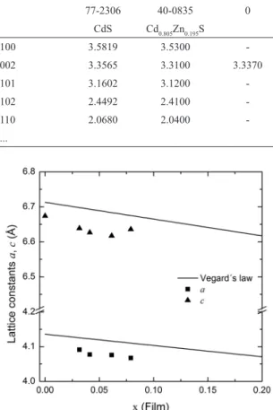
interplanar spacing d-values with those of PDF#77-2306 (CdS) and PDF#40-0835 (Cd0.805Zn0.195S) are shown. It has been observed that higher doped samples result in a phase change transition from hexagonal structure to cubic form, as a consequence of substitution of Cd2+ by Zn2+22.To obtain
more information about the ternary alloy structure, further analysis was carried out using Vegard’s law. Vegard’s law is an empirical rule that states that an alloy property value can be determined from a linear interpolation of the property values of its constituent elements. According to Vegard’s law22,23, lattice constants a and c of the Cd
1–xZnxS alloy
decrease linearly, whereas x increases from 0 to 1:
,
.
( )
Zn
Cit
ZnCit
k
s6 31
10
9
2 3 4
#
+
=
+ -
-On the other side, free Zn2+ ions react with OH- ions, to
form zinc hydroxide:
( )
Zn
2+QaqV+
2
OH
-QaqVZn OH
Q
V
2,QsV10
which can react with S2– ions to form ZnS:
( )
Zn OH
Q
V
2, aqQ V+
S
2-QaqVZnS
QsV+
2
OH
-QaqV11
Reaction (11) occurs because ksp for ZnS (10–25) is
much smaller than the ksp for Zn(OH)2 (10–16) and, from
ln(ksp) = ΔG0/RT, ZnS has a lower free energy change than
Zn(OH)2. According to Hodes 3, since CdS and ZnS have
diferent solubility product constants, the formation of a ternary compound would occur by precipitation of CdS, which adsorbs S2– and Zn2+ ions to form a ZnS layer. This
eventually difuses to form a solid solution of Cd1–xZnxS.
Figure 1 shows a schematic representation of Cd1–xZnxS
ternary compound precipitation. Side (A) corresponds to a process described above and side (B) corresponds to a process involving any hydroxide mechanism. According to reactions (6) and (10), Cd2+ and Zn2+ can react with OH– ions
to form metallic hydroxides. As the reaction proceeds, these metallic hydroxides transform to sulides as expressed by reactions (7) and (11). A diagram of species distribution was conducted to obtain a better understanding of the formation of Cd1–xZnxS through metallic hydroxide intermediates
species. Groups of intermediate chemical species formed during chemical reaction can be obtained from this diagram, bearing in mind that the dominant species depend strongly on chemical reagents used in the chemical bath.
In the reaction solution, Zn2+ and Cd2+ ions can react
with dissolved OH– and Cit3– ions to form several soluble
species, but our study is interested speciically in Zn(OH)2
and Cd(OH)2 species. Table 1 shows the chemical reactions
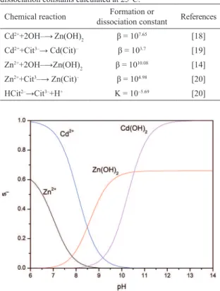
and their corresponding formation (β) and dissociation (K) constants at 25°C reported in literature. In all cases, the equilibrium constants were calculated by considering the concentration (mol×L–1), knowing that [OH–][H+]=10–14
mol×L–2, and taking Cd2+ as reference. Figure 2 shows
the repartition of species, si, as a function of pH. For a pH
between 8.5 and 10.5, Zn(OH)2 is the predominant species.
Above pH 10.5, the predominant species is Cd(OH)2. Thus,
at a pH of 11.5, Cd1–xZnxS ternary compound formation
proceeds via Cd(OH)2. This process is shown in Figure 1,
side (B), where it can be seen that Cd(OH)2 would adsorb
S2– and Zn2+ ions to form a ternary compound. It should also
be noted that, because of the lower ksp for Zn(OH)2 than for Cd(OH)2, growth may result through Zn(OH)2 species
afecting ilm properties as r increases.
Cd1–xZnxS ilm composition was determined by TXRF analysis (see Table 2). The ilm content (x) does not match that of the solution ratio r. Similar results have been reported
.
.
.
.
( )
x
x
a
c
4 136
0 325
6 713
0 479
12
=
-=
-Parameters a and c are related to the interplanar spacing d, as follows 24:
/
( )
d
h
hk
k
a c l
a
3
4
13
hkl
2 2 2 2
=
+
+
+
S
X
Q
V
Q
V
So, the d-spacing also shows a linear dependence on x. Figure 4 shows the variation in lattice constants a and c. A gradual decrease in lattice constants is observed as x increases. This trend is consistent with Vegard’s law and indicates a homogeneous alloy structure25. From Figure 4, a negative
Figure 1: Scheme of possibilities for coprecipitation of Cd1–xZnxS
thin ilms.
Table 1: Chemical reaction and their corresponding formation and
dissociation constants calculated at 25°C.
Chemical reaction dissociation constantFormation or References
Cd2++2OH–→ Zn(OH)
2 β = 10
7.65 [18]
Cd2++Cit3–→ Cd(Cit)– β = 103.7 [19]
Zn2++2OH–→Zn(OH)
2 β = 10
10.08 [14]
Zn2++Cit3–→ Zn(Cit)– β = 104.98 [20]
HCit2–→Cit3–+H+ K = 10–5.69 [20]
Figure 2: Distribution diagram of species for chemical bath solution
from Cd–Zn–H2O.
Table 2: TXRF analysis of Cd1–xZnxS thin ilms grown over 120 min.
r (Solution)
Element (at.%)
Cd Zn S (Film)x [S]/ [Zn+Cd]
Eg
(eV)
0 56.35 0 43.65 0 0.774 2.48
0.05 56.76 1.85 41.39 0.032 0.706 2.52 0.07 52.84 3.45 43.71 0.061 0.775 2.58 0.09 61.94 2.66 35.39 0.041 0.548 2.60 0.13 55.41 4.77 39.82 0.079 0.662 2.62
Figure 3: XRD patterns of Cd1–xZnxS ilms grown over 90 min.
several factors, including: (i) the relative size of constituent elements, (ii) the relative volume per valence electron and (iii) electrochemical diferences between the elements26. It has
been suggested in literature that deviations from Vegard’s law can be represented by a quadratic expression26,27; however,
applicability of such quadratic expression to any ternary alloys is unknown. Physically, deviations from Vegard’s law have been interpreted as a certain lattice disorder (related to
atom position) that produce a unit cell with volume either greater or smaller than that predicted from Vegard’s law27.
Another important parameter that can be calculated from XRD patterns is the crystallite size. In many cases, the crystallite size is calculated using Scherrer’s formula24;
however, such a formula considers that there is no lattice strain, and therefore peak broadening results only from the crystallite size efects. When lattice strains are expected to appear within the sample, the Williamson–Hall (W–H) plot allows for the separation of peak broadening when both microstructural causes – i.e., small crystallite size and microstrain – occur simultaneously28. Figure 5a shows the
W–H plot for samples with diferent Zn content (Zn = 0 is not considered). Bcosθ is a linear function of sinθ, which indicates that the lattice strain contributed signiicantly to peak broadening24. It can be seen from the slope of the linear
Table 3: Interplanar spacing dhkl of Cd1–xZnxS thin ilms.
hkl PDF# PDF# r ratio in reaction solution
77-2306 40-0835 0 0.05 0.07 0.09 0.13
CdS Cd0.805Zn0.195S
100 3.5819 3.5300 - 3.5446 3.5206 3.5276 3.5186
002 3.3565 3.3100 3.3370 3.3193 3.3087 3.3133 3.3179
101 3.1602 3.1200 - - - -
-102 2.4492 2.4100 - - - -
-110 2.0680 2.0400 - 2.0448 2.0435 2.0406 2.0364
...
Figure 4: Crystal lattice constants as a function of Zn ilm content (x).
Figure 5: a) Williamson–Hall plot and b) crystallite size as a
function of solution r ratio.
to peak broadening. The crystallite size calculated from the Y-intercept of the W–H plot is shown in Figure 5b as a function of r ratio in reaction solution. As r increases in solution, there is a clear decrease in crystallite size. This result could be a consequence of growth mechanism, which is favored by deposition conditions: a large concentration of OH– ions exists at pH 11.5; when Zn2+ is added to solution,
Zn(OH)2 forms according to reaction (10). When Zn(OH)2 protrudes from the solution to the substrate, the crystal size is not expected to change much with ilm thickness because the ionic exchange between OH– and S2– occurs instead of
another growth process. This could explain why the obtained crystallite size decreases as the Zn concentration increases.
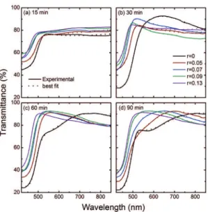
The thickness and optical properties of Cd1–xZnxS ilms were
obtained by analysing the corresponding optical transmittance spectra. In Figure 6, the transmittance spectra of Cd1–xZnxS
thin ilms deposited at diferent deposition times are shown. The absorption edge is at a.c. 500–520 nm in CdS ilms (x = 0), which agrees well with values reported in literature2,25.
As the Zn concentration increases in the Cd1–xZnxS ilms,
the absorption edge shifts to shorter wavelengths for all deposition times. The transmittance is between 75 and 90% at wavelengths longer than the absorption edge, which indicates that most incident light will be transmitted throughout the material. To estimate the ilm thickness and optical constants n and k, respectively, the transmittance spectra were itted to a layer model by considering the samples as constituted by an air/roughness/Cd1–xZnxS/glass system as reported in
refs13,14. The Cd
1–xZnxS optical constants were represented
by the SCI® model, which is a generalized version of the
Lorentz harmonic oscillator expression, consistent with the Kramers–Kronig relationships29. The model deines a
complex dielectric function ε= ε1+iε2, wherein ε1 and ε2 are
the real and imaginary part of the dielectric function, and is deined as follows:
( )
E E v E
A E E
14
*
center j
j center j
j m
1 2 2 2 2
2 2 2
1
f =
- +
-=
R
Q
Q
V
V
W" %
/
( )
E
E
v E
A Ev
15
*
center j j
j m
2 2 2 2 2
2
1
f
=
-
+
= "
Q
V
%/
if ε2 *>ε
1 *or E>E
center, then
( )
E 1 16
* *
1 1 2
f =f3Qf -f a + V
( )
E 17
* *
1 2 1
f =f3Qf -f a V
Else
( )
E 1 18
* *
1 1 2
f =f3Qf -f a + V
0
Figure 6: Optical transmittance spectra of Cd1–xZnxS deposited at
diferent deposition times, and diferent r ratios in reaction solution.
Where ε∞ is the high-frequency lattice dielectric constant, (Ecenter)j is the center energy of each oscillator which is related to the transverse phonon frequency. Aj is the amplitude (strength) of each oscillator and it is related to both the transverse and longitudinal phonon frequencies. vj is the vibration frequency (broadening) of the “j” oscillator. E is the energy and α is the damping coeicient. In the limit of α=0 the dispersión formula reduces to the Lorentz oscillator model. In the adjustment process are allowed to vary all parameters of the model to ind the best optimization given by values of root mean squared error (RMSE) less than 1. The model estimation of roughness was given by the thickness of this layer. In Figure 6, the dotted lines represent best its to the proposal layers model. Good agreement exists between experimental data and the theoretical it. From the itting procedure, the thickness, roughness and optical constants n and k for all the ilms were obtained. The roughness values ranged between 3 and 6 nm for all samples, and showed no clear trend with Zn ilm concentration.
In Figure 7, the ilm thickness is shown as a function of deposition time for all Cd1–xZnxS thin ilms. In the early
stages of deposition, up to 30 min, all Cd1–xZnxS ilms
exhibit a higher growth rate, which decreases as the r ratio in solution increases. After 30 min, the growth rate decreases in all cases. This occurs because of a decrease in reactant concentration as the reaction proceeds. Two interesting facts are that (i) the growth rate is slower as the Zn concentration in solution increases, (ii) the ilm thickness decreases as the Zn concentration increases. These two facts are related, and can be explained by considering the participation of a hydroxide growth mechanism. The decreasing thickness and growth rate are expected from the previously suggested hydroxide growth mechanism. Since initial hydroxide nucleation occurs homogeneously in solution, the compound is also formed
Figure 7: Film thickness as a function of deposition time and r
ratio in reaction solution.
homogeneously and therefore usually precipitates out in solution to a large extent. Thus, as the Zn concentration increases, this efect is expected to increase, which results in a slower ilm growth rate and therefore thinner ilms. The ilm thickness after 90 min deposition was a.c. 180 ± 0.7, 150 ± 0.3, 143 ± 0.3, 135 ± 0.2, and 125 ± 0.1 nm, for r = 0, 0.05, 0.07, 0.09, and 0.13, respectively.
The optical constants n and k as a function of the wavelength obtained from the itted transmittance spectra are shown in Figure 8 for thin ilms deposited during 90 min. As expected, the n spectra shape is similar to that obtained from analysis of an ellipsometric spectrum of CdS ilms reported previously in literature13,14. The maximum in the
n spectrum at ~480 nm (2.58 eV) for CdS ilms (x = 0) is related to optical transitions at a fundamental absorption edge of the CdS wurzite crystalline lattice. The position of the maximum in the n spectra indicates that the absorption edge is shifted to higher energy values for Cd1–xZnxS ilms. This
result matches a shift to higher energies of the absorption edge observed for Cd1–xZnxS ilms in the transmittance spectra.
The extinction coeicient spectra of the Cd1–xZnxS ilms
also show a shift to shorter wavelengths in the absorption region, as the Zn content increases in the ilms. This shift is related to the increase in band gap, as x increases. To estimate the energy band gap, Eg, of the ilms, the model for
allowed direct transitions between parabolic energy bands was used as given by30:
( )
hv
A
hv
E
/19
g1 2
#
a
Q
V
=
Q
-
V
/
( )
k
4
20
a
=
r
m
The α2 curve as a function of hν can be obtained by
considering the k spectra and equations (14) and (15). By extrapolating the linear portion of this curve to the x axis (where α2 = 0), the obtained result is hν = E
g.The calculated
band gap values are shown in Table 2. An increase in band gap with Zn content is observed, as expected from the formation of the Cd1–xZnxS ternary compound. The atomic percentage
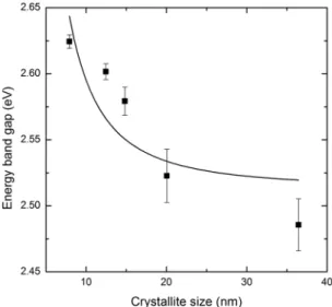
of Zn in the ilms does not exceed 4.77% (see Table 2), while a band gap value of 2.62 eV is reached. The same band gap value is reached, as reported by Carreón et al.8, when the
atomic percentage of Zn is 7%. This observation suggests that not only the concentration of alloy dopant is inluencing the band gap values. The dependence between band gap width and crystallite size has been investigated by several authors and attributed to quantum coninement efects31,32.
The latter occurs when the crystallite size is comparable with the Bohr exciton radius, where the continuum of energy levels is broken down into discrete states with an energy level spacing > kT, which results in a widening of band gap33. The
expected band gap resulting from quantum coninement is given by the following relation32:
( )
E
gE
gbulkE
b2
D
a
21
B 2
r
=
+
S
X
where Eg is the measured band gap energy value,
bulk g
E is
the expected bulk band gap energy value, Eb is the exciton
binding energy, aB is the exciton Bohr radius, and D is the average crystallite size (assumed to have a spherical shape), calculated from Scherrer’s formula. Crystallite size cannot be calculated from a W–H plot, when only one difraction peak appears (as occurs in the CdS sample). For this reason, in such a case, Scherrer’s formula has been used to estimate D. By adjusting the experimental data to Eg=A+B/D2, it is possible
to obtain the itting parameters A=Egbolk and B=4E bπ
2a2 B.
Figure 9 shows the relationship between band gap values and crystallite size, which has been obtained experimentally. From the itting process, the A and B parameters were 2.51 eV and 8.18 eV·nm2, respectively, and they agree well with
theoretical values (A = 2.42 eV and B = 9.60 eV·nm2 for
hexagonal CdS at room temperature32,34). The discrepancy
between calculated and theoretical B parameter may be attributed to several factors, such as the coulomb interaction between charge carriers, or the existence of intermediate or weak coninement32. The diference between calculated and
theoretical A is probably because of non-stoichiometric CdS ilms and the formation of ternary Cd1–xZnxS compound.
From these results, it can be concluded that the dependency of band gap on crystallite size may be attributed, in this work, to quantum coninement. Thus, the wide band gap exhibited by samples when compared with other work, could be related to a quantum coninement efect that results from a large reduction in crystallite size.
Figure 8: Refractive index (n) and extinction coeicient (k) as
a function of wavelength of Cd1–xZnxS with diferent r ratio in
reaction solution.
Figure 9: Energy band gap dependence of crystallite size for Cd1–xZnxS ilms.
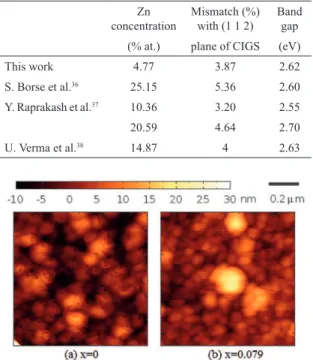
Table 4 compares the most noteworthy result obtained in this work with those reported in literature. In this work, a higher Eg value was reached with lowest Zn concentration,
which is a phenomenon attributed to a quantum coninement efect. The lattice mismatch between (1 0 0) hexagonal plane of Cd1–xZnxS (for the sample with 2.62 eV) and the (1 1 2)
tetragonal plane of CIGS (considering d(1 1 2) = 0.366 nm) was 3.8%. This value is the lowest calculated mismatch compared with those presented in Table 4. Thus, a low Zn concentration in Cd1–xZnxS ternary compounds will result
in a low lattice mismatch with absorbent CIGS layer and reduce losses in solar cell devices.
The surface morphology of Cd1–xZnxS thin ilms was
investigated by AFM. Figure 10 shows the AFM images of Cd1–xZnxS ilms deposited on a glass substrate for x = 0
Table 4: Comparison of Zn concentration, calculated mismatch
and band gap presented in this work with that reported in literature.
Zn
concentration Mismatch (%) with (1 1 2) Band gap (% at.) plane of CIGS (eV)
This work 4.77 3.87 2.62
S. Borse et al.36 25.15 5.36 2.60
Y. Raprakash et al.37 10.36 3.20 2.55
20.59 4.64 2.70
U. Verma et al.38 14.87 4 2.63
Figure 10: AFM surface images of Cd1–xZnxS ilms for (a) x = 0,
and (b) x = 0.079
size for samples containing Zn. This result agrees with the trend observed for optical constants (see Figure 8), since a smaller particle size produces more particle boundaries and results in a reduction in refractive index. A reduction in particle size is expected if we consider growth through M(OH)2 species (M = Zn or Cd), as mentioned previously.
Therefore, this result is further evidence that a hydroxide growth mechanism becomes important when Zn is added to the reaction solution.
4. Conclusions
From a study of low Zn–Cd1–xZnxS thin ilms grown using a free-ammonia chemical bath method, it is possible to conclude that:
- The grown mechanism of the ilm is afected strongly by Zn concentration in solution bath; as Zn increases, the hydroxide growth mechanism becomes important, and decreases the deposition rate and crystallite size of the thin ilms.
- Independent of the Zn concentration in the solution bath, and hence Zn ilm content, a hexagonal structure was obtained in all analyzed cases; as expected, only a small decrease in lattice parameter resulted as Zn content increased.
- Optical measurements revealed samples with a high optical transmittance (up to 90%). The band gap values increase up to 2.6 eV as Zn content in the ilm increased. This high band gap obtained with low Zn content in the ilm
(4.7 at.%) can be attributed to the presence of Zn and to quantum coninement efects since a decrease in crystallite size results from a change in grown mechanism.
It can be concluded that the main properties of the CdS window layer can be improved with small amounts of Zn in the ilm, which avoids an excessive mismatch with CIGS absorbent layer when in service, and improves device eiciency.
5. Acknowlegment
This work was supported by FONDECYT project N° 11090434, Grant CONICYT PFB-0824 and DIUC Project 210.011.050-1.0. C.A. Rodríguez appreciates the support provided by Conicyt through a Grant for Doctoral Thesis N° 21110556.
6. References
1. Kumar TP, Saravanakumar S, Sankaranarayanan K. Efect of annealing on the surface and band gap alignment of CdZnS thin ilms. Applied Surface Science. 2011;257(6):1923-1927.
2. Salem AM. Structure, refractive-index dispersion and the optical absorption edge of chemically deposited ZnxCd(1-x)S thin ilms.
Applied Physics A. 2002;74(2):205-211.
3. Hodes G. Chemical Solution Deposition of Semiconductor Films.
New York: Marcel Dekker; 2002.
4. Clayton AJ, Irvine SJC, Jones EW, Kartopu G, Barrioz V, Brooks WSM. MOCVD of Cd(1−x)Zn(x)S/CdTe PV cells using an
ultra-thin absorber layer. Solar Energy Materials and Solar Cells.
2012;101:68-72.
5. Devaney WE, Chen WS, Stewart JM, Mickelsen RA. Structure and properties of high eiciency ZnO/CdZnS/CuInGaSe2 solar cells.
IEEE Transaction on Electron Devices. 1990;37(2):428-433.
6. Chavhan SD, Senthilarasu S, Lee SH. Annealing efect on the structural and optical properties of a Cd1−xZnxS thin
ilm for photovoltaic applications. Applied Surface Science.
2008;254(15):4539-4545.
7. Gaewdang N, Gaewdang T. Investigations on chemically deposited
Cd1−xZnxS thin ilms with low Zn content. Materials Letters.
2005;59(28):3577-3584.
8. Carreón-Moncada I, González LA, Pech-Canul MI, Ramírez-Bon R. Cd1 − xZnxS thin ilms with low Zn content obtained by an
ammonia-free chemical bath deposition process. Thin Solid Films. 2013;548:270-274.
9. Burton LC, Hench TL. ZnxCd1–x S ilms for use in heterojunction
solar cells. Applied Physics Letters. 1976;29(9):612-614.
10. Reddy KTR, Reddy PJ. Studies of ZnxCd1-xS ilms and ZnxCd
1-xS/CuGaSe2 heterojunction solar cells. Journal of Physics D:
Applied Physics. 1992;25(9):1345-1348.
12. Rodríguez CA, Sandoval-Paz MG, Cabello G, Flores M, Fernández H, Carrasco C. Characterization of ZnS thin ilms synthesized through a non-toxic precursors chemical bath.
Materials Research Bulletin. 2014;60:313-321.
13. Sandoval-Paz MG, Sotelo-Lerma M, Mendoza-Galvan A, Ramírez-Bon R. Optical properties and layer microstructure of CdS ilms obtained from an ammonia-free chemical bath deposition process. Thin Solid Films. 2007;515(7-8):3356-3362.
14. Sandoval-Paz MG, Ramírez-Bon R. Analysis of the early growth mechanisms during the chemical deposition of CdS thin ilms by spectroscopic ellipsometry. Thin Solid Films.
2009;517(24):6747-6752.
15. Tec-Yam S, Rojas J, Rejón V, Oliva AI. High quality antirelective ZnS thin ilms prepared by chemical bath deposition. Materials Chemistry and Physics. 2012;136(2-3):386-393.
16. Treumann WB, Ferris LM. The determination of a thermodynamic stability constant for the cadmium citrate (CdCit-) complex ion at 25° by an E.M.F. method. Journal of Americal Chemical Society. 1958;80(19):5050-5052.
17. Martin RB. pH as a variable in free zinc ion concentration from zinc-containing lozenges. Antimicrobial Agents Chemotherapy.
1998;32(4):608-609.
18. Stipp SLS, Parks GA, Nordstrom DK, Leckie JO. Solubility-productconstant and thermodynamic properties for synthetic otavite, CdCo3(s), and aqueous associationconstnat for the
Cd(II)-CO2-H2O system. Geochimica et Cosmochimica Acta.
1993;57(12):2699-2713.
19. Qian JW, Tao Y, Zhang WJ, He XH, Gao P, Li DP. Presence of Fe3+ and Zn2+ promoted biotransformation of Cd–citrate complex
and removal of metals from solutions. Journal of Hazardous Materials. 2013;263(Part 2):367-373.
20. Roy P, Ota JR, Srivastava SK. Crystalline ZnS thin ilms by chemical bath deposition method and its characterization. Thin Solid Films. 2006;515(4):1912-1917.
21. Padam GK, Maholtra GL, Rao SUM. Studies on solution-grown thin ilms of ZnxCd1–xS. Journal of Applied Physics.
1988;63(3):770-774.
22. Azizi S, Dizaji HR, Ehsani MH. Structural and optical properties of Cd1-xZnxS (x = 0, 0.4, 0.8 and 1) thin ilms prepared using
the precursor obtained from microwave irradiation processes.
Optik - International Journal for Light and Electron Optics.
2016;127(18):7104-7114.
23. Hsiao CL, Palisaitis J, Junaid M, Persson POS, Jensen J, Zhao QX, et al. Room-temperature heteroepitaxy of single-phase Al1 − xInxN ilms with full composition range on isostructural
wurtzite templates. Thin Solid Films. 2012;524:113-120.
24. Dridi Z, Bouhafs B, Ruterana P. First-principles investigation of lattice constants and bowing parameters in wurtzite AlxGa1–xN,
InxGa1–xN and InxAl1–xN alloys. Semiconductor Science and
Technology. 2003;18(9):850-856.
25. Cullity BD, Stock SR. Elements of X-Ray Difraction. 3rd ed. London: Pearson; 2001.
26. Jana S, Maity R, Das S, Mitra MK, Chattopdhyay KK. Synthesis, structural and optical characterization of nanocrystalline ternary
Cd1–xZnxS thin ilms by chemical process. Physica E: Low-dimensional Systems and Nanostructures. 2007;39(1):109-114.
27. Jacob KT, Raj S, Rannesh L. Vegard’s law: a fundamental relation or an approximation? International Journal of Materials Research. 2007;98(9):776-779.
28. Murphy S, Chroneos A, Jiang C, Schwingenschlögl U, Grimes RW. Deviations from Vegard’s law in ternary III-V alloys.
Physical Review B. 2010;82(7):073201.
29. Zak AK, Majid WHA, Abrishami ME, Yousei R. X-ray analysis of ZnO nanoparticles by Williamson–Hall and size–strain plot methods. Solid State Sciences. 2011;13(1):251-256.
30. Zawaideh E, inventor. Nondestructive Optical Techniques for Simultaneously Measuring Optical Constants and Thicknesses of Single and Multilayer Films.United States Patent US 5889592. 1999 Mar 30.
31. Pankove JI. Optical processes in semiconductor. Mineola:
Dover Publications; 1976.
32. Cortés A, Gómez H, Marotti RE, Riveros G, Dalchiele EA. Grain size dependence of the bandgap in chemical bath deposited CdS thin ilms. Solar Energy Materials and Solar Cells. 2004;82(1-2):21-34.
33. Thangavel S, Ganesan S, Chandramohan S, Sudhagar P, Kang YS, Hong CH. Band gap engineering in PbS nanostructured thin ilms from near-infrared down to visible range by in situ Cd-doping. Journal of Alloys and Compounds. 2010;495(1):234-237.
34. Yofe AD. Low-dimensional systems: Quantum size efects and electronic properties of semiconductor microcrystallites (zero-dimensional systems) and some quasi-two-dimensional systems. Advances in Physics. 2002;51(2):799-890.
35. Nanda KK, Sahu SN. One-Dimensional Quantum Coninement in Electrodeposited PbS Nanocrystalline Semiconductors.
Advanced Materials. 2001;13(4):280-283.
36. Borse SV, Chavhan SD, Sharma R. Growth, structural and optical properties of Cd1−xZnxS alloy thin ilms grown by solution
growth technique (SGT). Journal of Alloys and Compounds.
2007;436(1-2):407-414.
37. Raviprakash I, Bangera KV, Shivakumar GK. Preparation and characterization of Cd1-xZnxS thin films by spry
pyrolysistechnique for photovoltaic applications. SolarEnergy.
2009;83(9):1645-1651.