DOI: http://dx.doi.org/10.1590/1980-5373-MR-2015-0058
Materials Research. 2016; 19(3): 669-672 © 2016
* e-mail: [email protected]
1. Introduction
Carbon ilms attract the scientiic interest because of their unusual structure and properties. They are typically denser, tougher and more resistant to chemical attacks than any other hydrocarbon or solid carbonaceous polymer1.
Graphene is a monolayer of carbon atoms arranged in a hexagonal lattice, and has attracted a great interest because of its unique structure and promising properties2. It is
extremely strong with a reported breaking strength of about 40 N/m and Young’s modulus of about 1 TPa3. It also exhibits
lexibility, it can crinkle and bend4. The presence of strains
in graphene can induce a pseudo-magnetic ield greater than 300 T5 and also changes its electronic structure6. The growth
of graphene cannot be described by a universal mechanism with speciic routes and conditions. Actually, there is a variety of synthesis strategies and growth modes7. A good
mechanism for its growth is the use of metal catalysts on which free carbon radicals are formed, carbon is dissolved in the catalyst, and inally precipitates and crystallizes at the surface8. It has been observed that an amorphous carbon
ilm is taken up by Fe, Co, or Ni ilms at temperatures above 600 °C9. The nucleation and subsequent growth of graphene
layers on the catalyst metal occur after the dissolution of the amorphous carbon ilm. The literature reports that the transformation of amorphous carbon to graphene occurs by diffusion of carbon atoms through the catalyst metal9.
The synthesis of graphene by epitaxial growth on transition metals has been previously reported10-13.
It has been observed that thin ilms produced by other processes such as chemical vapor deposition (CVD), are highly pure and present good quality crystal structures. However, the ilm stoichiometry and adhesion to the substrate is quite poor. On the other hand, high purity ilms cannot be produced by sputtering techniques because of the contaminated species in the plasma, which can be simultaneously deposited on the substrate, but good ilm adhesion to substrates can be obtained and the target stoichiometry is maintained in the deposited ilms. Such characteristics are achieved when co-deposition techniques (doping the ilms with other materials) are used.
Raman spectroscopy is one of the best-known techniques for graphite/graphene characterization. Raman spectra obtained from different regions of a carbon ilm deposited by magnetron sputtering showed 5 stages13 of growing
crystallization. The irst stage refers to the presence of disordered carbon atoms, the second one indicates a higher degree of crystallinity; the third one refers to single-crystalline graphite, the fourth one to the double layer graphene, and inally the ifth and last one to monolayer graphene13. These
spectra, when overlaid, show that there is a reduction in the D band, a narrowing, and intensity increase in the G band, and the arising of the 2D band, as the ilm crystallizes from amorphous to the monolayer graphene13.
In this work, the deposition of thin carbon ilm by magnetron sputtering on Co buffer layer previously deposited on heated sapphire substrates was performed aiming to obtain graphene layers.
Characterization of Thin Carbon Films Produced by the Magnetron Sputtering Technique
Danilo Lopes Costa e Silva a*, Luciana Reyes Pires Kassab b, Jose Roberto Martinelli a†,
Antonio Domingues dos Santos c, Sidney José Lima Ribeirod, Moliria Vieira dos Santos d
a Nuclear and Energy Research Institute, SP, Brazil b Faculty of Technology of São Paulo – FATEC-SP, SP, Brazil c Institute of Physics, University of São Paulo – USP, SP, Brazil
d Institute of Chemistry, São Paulo State University – UNESP,
CP 355, 14801-970, Araraquara, SP, Brazil
†In memorian
Received: January 21, 2015; Revised: March 22, 2016; Accepted: April 4, 2016
Thin carbon ilms containing both amorphous and crystalline structures were produced by RF magnetron sputtering. The depositions of the carbon ilms were performed on Co buffer layers previously deposited on c-plane (0001) sapphire substrates. The thin carbon ilms were characterized by high-resolution transmission electron microscopy (HRTEM), X-ray diffraction (XRD), Raman spectroscopy, energy dispersive X-ray spectroscopy (EDS), and ield emission scanning electron microscope (FEG-SEM). The Raman spectra conirmed the presence of amorphous and crystalline structures by the existence of an intense D band separated from the G band, indicating early stages of crystallization. The interplanar distance corresponding to the graphite structures was determined by using HRTEM micrographs.
Costa e Silva et al.
670 Materials Research
1. Materials and methods
1.1 Deposition
The carbon/cobalt depositions were performed using an ATC 2000 Sputtering System (Aja International equipment) by DC magnetron sputtering technique from a 99.999% pure Kurt J. Lesker graphite target, and a 99.99% pure cobalt target, respectively. The substrate was sapphire orientated on c-plane (0001), 1x1 cm2, and the substrate/target distance
was kept at 15 cm. The rotating substrate-holder was kept at 600°C by thermal radiation from internal incandescent lamp bulbs during the whole process. The pressure before inserting a mixture of Ar and 5% of H2 was 2 x 10
-7 Torr.
The deposition of Co was carried out during 16 minutes, with the DC power supply set to 100 W, working pressure of 5 mTorr and gas low of 20 sccm. For the C deposition, during 1 hour, the DC power was 150 W, the working pressure was 15 mTorr and the gas low was 40 sccm. A heat treatment was performed in a Lindberg/Blue tube furnace under a 2.85 x 10⁻⁵ Torr, using an Oerlikon Leybold vacuum Pump
System PT50, during 10 minutes at 850 °C.
1.2 Characterization
The morphological characterization of the samples was performed using a ield emission gun scanning electron microscope (FESEM, JEOL JSM-7500F), and a high-resolution transmission electron microscope (HR-TEM JEOL 3010), 300 kV with LaB6 ilament). The structural characterization
was performed by a Minilex II Rigaku X-Ray Diffractometer equipment with KαCu radiation and the Raman spectroscopy by a HORIBA JOBIN–YVON model LabRAM HR 800 spectrometer, operating with laser He–Ne 632.81 nm with a CCD camera model DU420AOE-325.
For the measurement of the carbon thin ilm thickness it was used the Rutherford Backscattering Spectrometry (RBS) and the Nuclear Reaction Analysis (NRA) for the nuclear reaction 12C(4He,4He)12C, at the alpha beam energy of 4.256 MeV. The spectrum was analyzed with the aid of the SIMNRA15. This measurement was performed for
a carbon ilm produced with the same deposition conditions described above (C deposition during 1 h with RF power of 150 W) on (100) Si substrate and it was obtained 2.6 nm for the C thickness.
2. Experimental results and discussion
2.1 Morphological studies
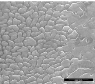
Figure 1 shows the FEG-SEM micrograph of one of the carbon/cobalt deposited sample on a c-plane (0001) sapphire substrate, keeping the substrate heated, as previously described. The partial coalescence of Co grains can be seen.
2.2 HRTEM and EDS
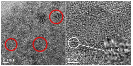
High-resolution transmission electron micrographs (HRTEM) are shown in Figures 2a and 2b of two different regions of the C/Co surface after heat treatment. In Figure 2a, crystalline structures (red circles) related to the cobalt ilm can be seen. The method used for the preparation of the sample for the HRTEM was based on scrapping the sample with a quartz point and depositing it on the HRTEM grid. Figure 2b
shows a material that has been reported in the literature14 as
“Onion-Like-Carbon (OLC)”, where several carbon planes are rolled forming a circular structure, which resembles an onion with its concentric layers. The curving and closure of these newly formed graphitic planes occurs to minimize their surface energy14. Figure 2c shows the EDS spectrum of
the “Onion-Like-Carbon” structures (Figure 2b). The intense carbon peak conirms the composition of the “onion-like” structures. The presence of a Cu peak is related to the grid used for HRTEM measurements. O and Si peaks are probably due to contamination during the sample preparation for HRTEM measurements. The interplanar distance shown in Figure 2b was measured by the use of the ImageJ software. The obtained value is in the range of 0.345 to 0.350 nm and corresponds to the interplanar distance of graphite, as previously reported in the literature.
2.3 – Films’ crystallinity
The crystallinity of the carbon ilm was investigated by the XRD measurements. In the XRD pattern shown in Figure 3, there is a peak at ~ 2θ = 26.5° (ICSD 01-089-8487) that can be associated to the presence of graphite structures. There is also a peak related to the sapphire substrate (Al2O3)
at 2θ = 20.5° (ICSD 01-073-1199). The XRD measurements were conducted in the theta-2theta coniguration and the results corroborates the Raman spectra (see next section), where there is a band related to crystalline carbon ilms and another band to amorphous ones.
2.4 – Raman spectroscopy
Figure 4 shows the Raman spectrum corresponding to the carbon ilm deposited on sapphire substrate heated at 600 °C and working pressure of 15 mTorr.
Comparing the spectra previously reported13 with those
Characterization of Thin Carbon Films Produced by the Magnetron Sputtering Technique
2016; 19(3) 671
Fig. 2 – (a) HRTEM image of the sample treated in high vacuum showing crystalline structures related to cobalt randomly distributed; (b) HRTEM image of another region of the sample, where there is the presence of “Onion-Like-Carbon” structures; (c) EDS spectrum of the structures shown in Figure 2b.
Fig. 3 - X-Ray diffraction pattern of the sample that underwent heat
Costa e Silva et al.
672 Materials Research
carbon) is more intense than the G band (vibrational mode of ordered carbon), and the 2D band that normally appears for graphite and graphene ilms, being much more intense than G band for the monolayer graphene structure. Normally, the 2D and G bands have the same intensity for bilayer graphene structure.
3. Conclusions
In this work, evidences are shown that carbon ilms deposited by magnetron sputtering on Co buffer layers previously deposited on heated sapphire substrates present amorphous and crystalline regions. This could be conirmed by the Raman spectrum that shows the D band related to amorphous carbon, but also the G and 2D bands related to crystalline carbon structures. The XRD patterns evidenced the presence of graphite and the HRTEM micrographs indicated the presence of graphite planes and OLC structures whose interplanar distances were measured. There is a strong
motivation for further research to obtain graphene, by adjusting the parameters used for magnetron sputtering. This process may become an alternative method for the production of crystalline carbon ilms, controlling the number of layers of graphene ilms, in order to use them in advanced scientiic researches and applications.
Acknowledgements
This work was supported by the National Institute of Photonics (INCT de Fotônica) project granted by the Conselho Nacional de Desenvolvimento Científico e Tecnológico - CNPq. We would like to thank FAPESP, Laboratório Nacional de Nanotecnologia do Centro Nacional de Pesquisa em Energia e Materiais, for the HRTEM measurements and Laboratório de Materiais e Feixes Iônicos do Instituto de Física da USP for the RBS/NRA measurements.
References
1. Amorim HA. Caracterização de ilmes inos de carbono depositados por PECVD, [Dissertation]. Campinas (SP): UNICAMP; 1995.
2. Geim AK, Novoselov KS. The rise of graphene. Nature Materials.
2007;6:183-191. http://dx.doi.org/10.1038/nmat1849 3. Lee C, Wei X, Kysar JW, Hone J. Measurement of the elastic
properties and intrinsic strength of monolayer graphene.
Science. 2008;321(5887):385-388. http://dx.doi.org/10.1126/
science.1157996
4. Booth TJ, Blake P, Nair RR, Jiang D, Hill EW, Bangert U, et al. Macroscopic graphene membranes and their extraordinary stiffness. Nano Letters. 2008;8(8):2442-2446. http://dx.doi.
org/ 10.1021/nl801412y
5. Levy N, Burke SA, Meaker KL, Panlasigui M, Zetti A, Guinea F, et al. Strain-induced pseudo–magnetic fields greater than 300 tesla in graphene nanobubbles. Science.
2010;329(5991):544-547. http://dx.doi.org/10.1126/science.1191700.
6. Huang M, Yan H, Heinz TF, Hone J. Probing Strain-induced electronic structure change in graphene by Raman spectroscopy.
Nano Leters. 2010;10(10):4074-4079. http://dx.doi.org/10.1021/
nl102123c
7. Subrahmanyam KS, Vivekchand SR, Govindaraj A, Rao CN. A study of graphenes prepared by different methods: characterization, properties and solubilization. Journal of Materials Chemistry.
2008;18(13):1517–1523. http://dx.doi.org/10.1039/B716536F 8. Barreiro A, Börrnert F, Avdoshenko SM, Rellinghaus B,
Cuniberti G, Rümmeli MH, et al. Understanding the catalyst-free transformation of amorphous carbon into graphene by
current-induced annealing. Science Reports. 2013;1115. http:// dx.doi.org/10.1038/srep01115
9. Rodríguez-Manzo JA, Pham-Huu C, Banhart F. Graphene growth by a metal-catalyzed solid-state transformation of amorphous carbon. ACS Nano. 2011;5(2):1529–1534. http://
dx.doi.org/10.1021/nn103456z
10. N’Diaye AT, Bleikamp S, Feibelman PJ, Michely, T. Two-Dimensional Ir Cluster Lattice on a Graphene Moiré on Ir(111).
Physical Review Letters. 2006;97(21):215501. http://dx.doi.
org/10.1103/PhysRevLett.97.215501
11. Marchini S, Gunther S, Wintterlin J. Scanning tunneling microscopy of graphene on Ru (0001). Physical Review B.
2007;76(7):075429. http://dx.doi.org/10.1103/PhysRevB.76.075429 12. Vazquez de Parga AL, Borca FC, Passeggi MC Jr, Guinea
JJ, Miranda R. Periodically rippled graphene: growth and spatially resolved electronic structure. Physical Review Letters. 2008;100(5):056807. http://dx.doi.org/10.1103/
PhysRevLett.100.056807
13. Yurkov AN, Melnik NN, Sychev VV, Savrans VV, Vlasov DV, Konov VI. Synthesis of carbon films by magnetron sputtering of a graphite target using hydrogen as plasma-forming gas.
Bulletin of the Lebedev Physics Institute. 2011;9:263.
14. McDonough JK, Gogotsi Y. Carbon onions: synthesis and electrochemical applications. The Electrochemical Society Interface. 2014:23(1):61-65.