Development of stable current collectors for large area
dye-sensitized solar cells
Ana Isabel Pereira1, Jorge Martins1, Carlos José Tavares2, Luísa Andrade1, Adélio Mendes1* 1LEPABE, Departamento de Engenharia Química, Faculdade de Engenharia, Universidade do Porto, Rua Dr. Roberto Frias, 4200-465 Porto, Portugal
2Centro de Física, Universidade do Minho, Campus de Azurém, 4804-533 Guimarães, Portugal * Corresponding Author: [email protected]
Keywords Large area DSC Photoelectrochemical Sputtering Sheet resistance Tungsten Indium-Tin Oxide
Abstract
The substrate sheet resistance effect in a large area dye-sensitized solar cell (DSC) device is still the main factor responsible for low energy conversion efficiencies. In this work, current collectors made of metal lines were applied by magnetron sputtering on a transparent conducting glass substrate. The introduction of these metal lines enabled a decrease in the sheet resistance from 7.26 Ω·□-1 to 2.52 Ω·□-1, by depositing an optimized 1.0 μm tungsten thick layer on the top of 1.5 μm thick molybdenum lines. These Mo/W lines withstanded long-term stability when in contact with iodide/triiodide redox couple. Large area dye-sensitized solar cells with 36 cm2 of active area were assembled and the power conversion efficiency increased from 0.54 % to 1.62 % when ten metal lines were applied in both electrodes. As a final design, Mo/W lines were only applied onto the counter-electrode and protected with an indium-tin oxide layer; the resulting device showed a power conversion efficiency of 3.43 %, compared with the reference efficiency of 2.38 %.
1. Introduction
Dye-sensitized solar cells (DSCs) have attracted significant industrial interest in the last decades for the conversion of solar light into electricity, specially due to its simple manufacture process and low cost [1]. A DSC consists of two electrodes, the photoelectrode (PE) that is composed by a dye-sensitized mesoporous TiO2 film, and the counter-electrode (CE) that is made of a platinum catalyst thin layer; between them there is an electrolyte, typically containing the iodide/triiodide (I-/I
3-) redox couple in a liquid solution [2]. While the highest certified power conversion efficiency (PCE) is 11.9 % for a cell of 1.005 cm2 it was reported recently a lab size DSC with 14.3 % [3]. At larger-scale, the record PCE value of 10.7 % was reached for a mini-module of 7 cells connected in series with a total area of 26.55 cm2 and a PCE of 8.8 % for a sub-module of 398.8 cm2 with 26 serial cells, both by Sharp [4]. This power conversion efficiency difference between lab and industrial scale is a major limitation for all photovoltaic technologies and in particular for DSCs.
When large area glass substrates are used, typically coated with a transparent thin layer of fluorine doped tin oxide (FTO), the effect of ohmic resistance increases. As the active area of DSC increases, the short circuit current (JSC) and the fill factor (FF) decreases, leading to a drop in conversion efficiency [5, 6]. Electrochemical impedance spectroscopy studies and other dynamic characterization techniques revealed changes in the charge transport and recombination as the photoelectrode area increases. After injection into the semiconductor layer electrons face an increased transport resistance, which favors electron recombination with redox ions (I3-) present in the electrolyte [7, 8]. Therefore, when large area DSCs are prepared, the charge collection efficiency becomes more significant when compared with smaller single cells.
Moreover, the ohmic resistance in a DSC substrate also depends on the cell geometry and it should be optimized to obtain high fill factors. Always, bearing in mind a simple cell design, to ensure the aesthetic aspect of the produced modules. Many solutions have been proposed to compel
special attention to cells configuration and materials performance, namely, the use of large size submodules composed of multiple small area cells. However, due to the high number of small cells the aperture ratio (ratio between active and total area) is quite low [9]. Decreasing the internal ohmic resistance of a large area substrate in a DSC and maintaining the recombination rate independent of the area is crucial to guarantee high photovoltaic performance [10], but also very desirable for building integrated applications, enabling simpler architectures and for lower production costs [9].
The most obvious way for reducing the internal ohmic resistance of a DSC is by introducing current collectors such as metal colleting grids, in analogy with conventional photovoltaic cells. Though, for DSC applications, the selection of the current collector materials should be carefully studied due to the highly corrosive nature of I-/I
3- redox couple and the ability of occurring charge recombination in the metal grids/electrolyte interface (dark current), responsible for a reduced cell photocurrent [10]. Materials like nickel, titanium, silver, aluminum and stainless steel have been studied on large area DSCs, but in most of cases a protection layer made of a resin or a glass-ceramic is needed, albeit leading to complex and expensive manufacturing processes [9-15]. Recently, Jihuai et al. prepared a PEDOT-Pt/Ti counter-electrode, where PEDOT-Pt was electrodeposited over a Ti-mesh. The photoelectrode consisted in a 100 cm2 Ti foil substrate. The prepared devices showed higher energy conversion efficiencies for large cells (PCE = 6.69 %).
Within this work, two metals are investigated as current collectors for large area DSCs: tungsten and molybdenum. These two materials exhibit high resistance against electrolyte corrosion over a long time, suitable work functions to create an ohmic contact with TiO2 photoelectrode and good sheet resistance values [2, 16, 17]. The current collectors in the form of metal lines were prepared using different combinations of molybdenum and tungsten. First, the materials morphology was studied and characterized aiming the optimization of the deposition procedures and then the prepared conductive lines were applied on complete large area DSC devices for photovoltaic performance assessment.
2. Experimental
2.1 Preparation of current collectors
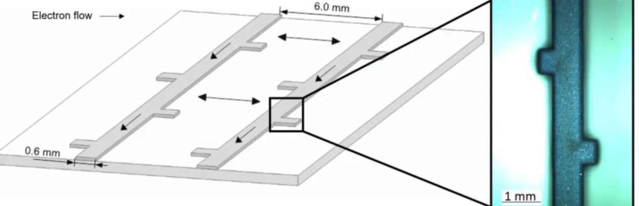
The current collectors were deposited directly on top of 8 × 8.5 cm2 transparent conductive oxide (TCO) coated-glass, 2.2 mm thick and sheet resistance of 7 Ω∙□-1, from Solaronix®, as shown in Fig. 1. The glass substrates were first washed as described elsewhere [18]. Then a metal mask was placed on top of the TCO glass substrate with the help of a double sided Kapton® tape.
Fig. 1 Left: Current collectors design deposited on top of a TCO glass substrate (not drawn in scale). Right: Top view optical microscopy image of a current collector.
The deposition of molybdenum and tungsten was made by magnetron sputtering (QPrep400 from Mantis Deposition®), a type of physical vapor deposition (PVD). This method consists in bombarding the target (Mo or W, respectively) with energetic argon ions and subsequent ejection of neutral metal atoms species that condense as a growing film on the substrate. For the depositions, the following conditions were used: 10-4 Pa of base pressure; 20 sccm of argon flow, where the argon pressure was controlled by the throttle valve; a bias potential of -50 V applied to the substrate; and a substrate rotation speed of 6 rpm. A quartz crystal monitor (QCM) was used to measure the thickness of the conductive lines during depositions. The sample holder had a capacity for 9 glass substrates. The deposited metal line properties were optimized changing by the argon pressure (PAr) and substrate temperature (TSubstrate).
The electrical resistance of the lines (RLine) was measured using a two-point probe technique with test probes placed ~7 cm apart, being averaged on 10 sampling values. For each sample, 10 lines were deposited with a length of 77 mm and a width of 0.6 mm, spaced 6 mm from each other. Sheet resistance measurements were performed using a four-point probe technique, following the Van der Pauw method, always for the same analyzed area.
A binocular stereo optical microscope (OPTIKA Italy) and scanning electron microscope (FEI Quanta FE-SEM) were used to characterize the morphology of conductive lines. X-ray diffraction (Bruker AXS D8 Discover) was employed to analyze the crystalline structure of the conductive lines. Inductively coupled plasma mass spectrometry (ICP-MS Thermo Scientific) characterization was performed to assess the corrosion of the lines when exposed to the redox electrolyte solution.
2.2 Large area DSC device assembly
For large area DSC photovoltaic performance assessment, two-sized devices were prepared with 6 × 6 cm2 and 2 × 2 cm2 of active area; the cell assembly procedure was the same for both sizes. The photoelectrodes were prepared as described elsewhere [18]. Briefly, the glass substrates were treated with a 40 mM TiCl4 aqueous solution at 70 °C for 30 minutes followed by three cycles of screen printing of TiO2 paste (Ti-Nanoxide T/SP from Solaronix®), alternating with drying at 100 °C for 10 minutes. The samples were then sintered at 500 °C for 30 minutes and the final photoelectrode thickness was 12 µm. The counter-electrode glass substrates were drilled with four holes with 1 mm diameter each and the platinum paste (Platisol T/SP from Solaronix®) was then screen printed and sintered at 450 °C for 15 minutes. Both electrodes were sandwiched and sealed with thermoplastic sealant with 60 µm thick (Surlyn® from Solaronix®) in a hotpress at 175 °C for 15 seconds; the final interdistance between the two glass substrates was ~30 µm. Dye adsorption in the porous TiO2 photoelectrode was enabled by recirculation the dye solution (1 mM of N719 from Solaronix® in ethanol) for 14 hours using a peristaltic pump (Ismatec® Ecoline). The photoelectrode was then rinsed with ethanol, dried with nitrogen and the electrolyte
(Iodolyte Z-150 from Solaronix®) filled through the aforementioned holes, which were subsequently closed with Surlyn® and glasses slides. Finally, silver paste (RS Components) was applied onto the electrical contacts. Half-cells devices of 2 × 2 cm2 were also prepared to characterize the counter-electrode, as described elsewhere [19].
2.3 Device characterization
I-V characteristics were obtained using an electrochemical station (Autolab, PGSTAT302N). The
cells were front illuminated using a solar simulator (Newport, USA) calibrated using a single crystal Si photodiode (Newport, USA); 1-sun incident radiation was used, equivalent to 1000 W∙m-2. Electrochemical impedance spectroscopy (EIS) measurements were performed in the dark within a frequency range from 100 kHz to 0.05 Hz, with an AC modulation of 10 mV; commercial software ZView® (Scribner Associates Inc.) was used.
3. Results and discussion
3.1 Mo/W lines deposition
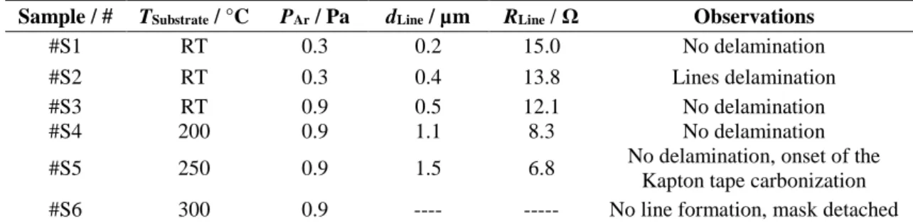
Deposition of tungsten films and their characterization have been extensively reported in the literature. The properties of the film strongly depend on the deposition process as well as on the purity [20-23]. The tungsten deposition parameters were optimized to maximize the adhesion of W lines to the TCO layer and to minimize RLine. It was observed that the operating conditions that mostly affect the lines properties were TSubstrate and PAr during the deposition. Table 1 shows different operating conditions tested for the deposition of W lines.
Table 1 Operating conditions of tungsten deposition with the correspondent thickness (dLine) and electrical
resistance of the line (RLine).
Sample / # TSubstrate / °C PAr / Pa dLine / µm RLine / Ω Observations
#S1 RT 0.3 0.2 15.0 No delamination
#S2 RT 0.3 0.4 13.8 Lines delamination
#S3 RT 0.9 0.5 12.1 No delamination
#S4 200 0.9 1.1 8.3 No delamination
#S5 250 0.9 1.5 6.8 No delamination, onset of the
Kapton tape carbonization #S6 300 0.9 ---- --- No line formation, mask detached
As expected, increasing the thickness of the tungsten lines favors the decrease of RLine, however the film adhesion (delamination) is affected mainly due to residual stress formed during the deposition. Delamination was minimized increasing the PAr from 0.3to0.9Pa, which makes the residual stress to change from compressive to tensile [24]. Moreover, increasing the substrate temperature allows growing thicker films without delamination since higher temperature induces a residual stress relaxation and concomitant decrease in RLine. However, this temperature increase was limited by the thermal decomposition of the Kapton® tape at ca. 250 °C. From Table 1, the operating conditions of sample #S5 gives the lowest RLine and the best adhesion to the TCO glass substrate, respectively 6.8 Ω of RLine and 1.5 µm thick. Since thicker tungsten lines are difficult to obtain, it was assessed a different metal line configuration aiming to decrease further the electrical resistance; a bilayer configuration of molybdenum and tungsten (deposited using the optimized parameters in Table 1) was then tested – Table 2.
Table 2 Combinations of molybdenum (Mo) and tungsten (W) materials and the correspondent electrical resistance (RLine).
Sample / # Materials combinations / µm RLine / Ω Observations
1#1.5Mo 1.5 µm Mo 4.9 Good adhesion, no delamination
2#1.0W 1.0 µm W 8.3 Poor adhesion, no delamination
3#1.5W 1.5 µm W 6.8 Poor adhesion, some delamination
4#1.5Mo1.0W 1.5 µm Mo + 1.0 µm W 4.2 Good adhesion, no delamination
5#1.5Mo1.3W 1.5 µm Mo + 1.3 µm W 3.6 Good adhesion, some delamination
Comparing single molybdenum and tungsten lines with the same thickness, samples 1#1.5Mo and 3#1.5W, molybdenum gives lower electrical resistance and better adhesion. However, as-prepared molybdenum and tungsten lines were submitted to dipping tests in the electrolyte solution over a month to evaluate their corrosion resistance. Molybdenum lines were completely dissolved, contrary to what has been reported before [16, 17]. On the other hand, tungsten lines showed excellent corrosion resistance to the electrolyte. Combining the two materials in a layered metal line, where tungsten coats molybdenum, thicker and then more conductive metal lines can be obtained and corrosion resistant. Even though sample 5#1.5Mo1.3W presents the lowest RLine, the adhesion to the substrate was better for sample 4#1.5Mo1.0W. Since the thickness of tungsten
was lower; this limits the quality of the adhesion and consequently of the current collector. Both 4#1.5Mo1.0W and 5#1.5Mo1.3W samples exhibit the lowest RLine and for that reason these samples were applied in substrates of 36 cm2 active area - Section 3.3.
3.2 Mo/W lines characterization
After optimizing the current collectors deposition in terms of adhesion and electrical resistance, the combined Mo/W lines were further characterized. For that, TCO glass substrates with dimensions of 8 × 8.5 cm2 were prepared with 10 conductive lines. Sheet resistance (R
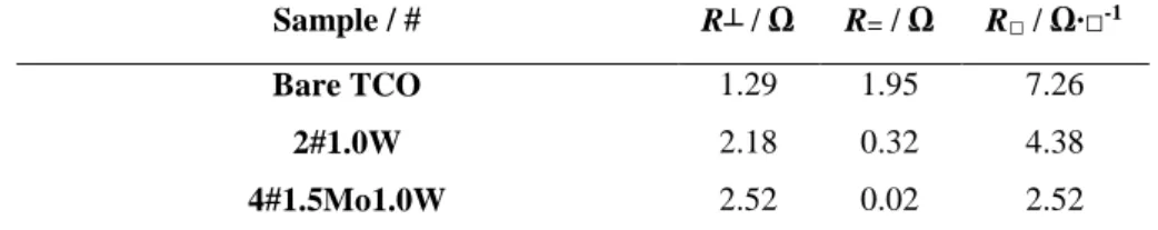
□) measurements, i.e. the electrical resistance of the TCO glass substrate with coated metal lines, were performed using Four-point probe measurements following the Van der Pauw method was used, where R┴ was measured in the perpendicular direction of the lines and R═ in the parallel direction [25] – Table 3. For bare TCO glass substrate (without conductive lines), R┴ and R═
values are similar showing no preferential direction for the electron flow. When 10 lines with 1.0 µm of tungsten were added to the TCO glass substrate, R═ decreases from 1.95 Ω to 0.32 Ω, whereas R┴ increases from 1.29 Ω to 2.18 Ω; as expected, the electron flow became preferential in the parallel direction of the lines. Combined Mo/W lines present an even lower R═ (0.02 Ω) and a highest R┴(2.52 Ω), resulting in the lowest sheet resistance obtained, R□ = 2.52 Ω·□-1. The sheet resistance stability of the combined Mo/W lines to a thermal treatment at 500 °C during 30 min was assessed; this treatment simulates the TiO2 photoelectrode sintering process. This test showed that the sheet resistance after the heat treatment remains almost unchanged (2.67 Ω∙□-1).
Table 3 Four-point probe measurements of different conductive lines on 8 × 8.5 cm2 TCO glass substrates. R
was measured in perpendicular direction to the lines, whereas R=was measured in parallel direction to the lines.
Sample / # R┴ / Ω R= / Ω R□ / Ω∙□-1
Bare TCO 1.29 1.95 7.26
2#1.0W 2.18 0.32 4.38
4#1.5Mo1.0W oxidized at 500 °C 2.48 0.04 2.67
Fig. 2 illustrates the electron pathways when an electrical field is applied across the substrates. For a bare TCO glass substrate electron transport is only carried through the film – Fig. 2A. Adding conductive lines, a new electric pathway emerges: electrons converge to the conductive lines from the sides, as shown by the four-point probe measurements – Fig. 2B-C. The top surface area of the conductive metal lines can be conductive – Fig. 2B – or non-conductive – Fig. 2C, as it happens after annealing the substrate and metal oxide is formed. However, since the top metal surface area is small compared to the whole substrate area, there are no significant differences between these two cases when inserted in a DSC device, the electrical transport in TCO should remain.
Fig. 2 Schematic representation of charge pathways in A: bare TCO glass substrate; B: TCO glass substrate with Mo/W lines; C: TCO glass substrate with an oxide layer formed on the top of the Mo/W lines after heat treatment.
The morphology of the conductive lines was analysed by scanning electron microscopy (SEM) - Fig. 3. A SEM image of the Mo/W line cross-section is presented, Fig. 3A, revealing a good adhesion between the TCO glass substrate. Also, the morphology shows a compact structure, crucial to obtain low electrical resistance [26]. Fig. 3B shows the top view of the as-deposited Mo/W lines. The morphology of the metal lines is affected mainly by two reasons: the TCO glass substrate roughness and the shadow effect caused by the mask used. Looking closely to the cross
section image (Fig. 3A), a laminar slanted grain structure is apparent, which should result from the angle of incidence. Top view micrograph of the Mo/W lines after a heat treatment at 500 °C during 30 minutes, Fig. 3C, shows larger crystals suggesting the presence of tungsten oxide.
Fig. 3 SEM micrographs for deposited Mo/W lines on TCO glass substrate: A: cross-section; B: top view for as-deposited; C: top view after heat treatment at 500 °C during 30 minutes.
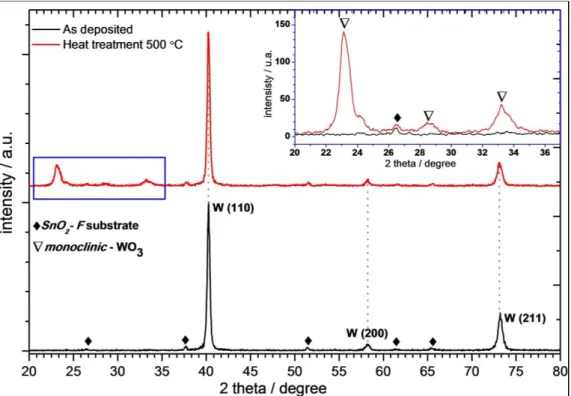
The chemical composition of the thermally treated tungsten lines was compared with untreated lines using X-ray diffraction. Fig. 4 shows the diffraction patterns for tungsten with no heat treatment (black line), revealing a α-W phase with a body-centered cubic structure and presenting characteristic diffraction peaks from the (110), (200) and (211) reflection planes. After heat treatment, it is possible to see emerging peaks that can be attributed to monoclinic tungsten trioxide (WO3) phase. The analysis of the characteristic diffraction peaks suggests the presence of two characteristic triplets, consisting in (002), (020) and (200) reflections between 22.1-24.6°, and (022), (-202) and (202) reflections between 31.9-34.9°. However, tungsten metal continues to be the main fraction of the sample.
Fig. 4 X-ray diffraction patterns of tungsten lines deposited on top of a TCO glass substrate (black line) and after a heat treatment at 500 °C during 30 minutes (red line). Inset figure shows a zoom to distinguish monoclinic-WO3 characteristic peaks
ICP-MS measurements were performed to analyse metal corrosion in the redox electrolyte (I-/I 3-). The stability in the presence of the electrolyte of a sample with a 1.0 µm thick tungsten line (Sample 2#1.0W) and a sample with composite Mo/W lines (Sample 4#1.5Mo1.0W) was assessed; molybdenum lines proved to be unstable in the presence of the electrolyte – see section 3.1. Table 4 shows the concentration of dissolved metals after 7 and 37 days of dipping time. Tungsten lines did not corrode even after 37 days; ICP-MS measurements showed values of dissolved tungsten in the electrolyte below the detection limit of the equipment. Concerning the sample with a Mo/W line, the ICP-MS measurements showed a concentration of 0.6 mg∙L-1 of dissolved molybdenum after 7 days, maintaining the same value after 37 days. This provides evidence that the tungsten protective layer has a significant ability to protect the underlying molybdenum layer from corrosion.
Table 4 – ICP-MS analysis of I-/I
3- redox electrolyte after dipping of conductive lines during 7 and 37 days. Sample Element After 7 days / mg∙L-1 After 37 days / mg∙L-1
2#1.0W W < 0.2 < 0.2
4#1.5Mo1.0W Mo 0.6 0.6
3.3 Large area DSC characterization
A series of DSC devices were prepared incorporating the developed conductive lines in both substrate sides and characterized in terms of photovoltaic performance - Fig. 5 and Table 5.
Fig. 5 I-V characteristics for small (SR) and large (LR) DSC reference cells without conductive lines and DSC devices with different combinations of Mo/W lines.
Table 5 I-V parameters for small (SR) and large (LR) DSC reference cells without conductive lines and DSC devices with different combinations Mo/W lines.
Device Active area / cm2 VOC / V JSC / mA∙cm2 FF η / %
SR cell 0.196 0.73 10.03 0.65 5.02
LR cell 36.0 0.70 3.05 0.25 0.54
4#1.5Mo1.0W 32.4 0.65 4.45 0.49 1.42
Two DSC reference cells were considered: a small circular (SR cell) of 0.196 cm2 and a large one with 6 × 6 cm2 without conductive lines (LR cell); when Mo/W lines are applied the active area decreases from 36 cm2 to 32.4 cm2 due to the shadow caused by the lines. As expected, it was observed a significant difference on the power conversion efficiency between the two cells. Concerning the devices incorporating Mo/W lines, with 4#1.5Mo1.0W and 5#1.5Mo1.3W devices, it was observed a power conversion efficiency enhancement from 0.54 % (LR cell) to 1.42 % (4#1.5Mo1.0W) and further increased to 1.62 % (5#1.5Mo1.3W); the photovoltaic performance enhancement occurred mainly due to JSC and FF improvement. The current density
increases approximately proportionally to the sheet resistance decrease.
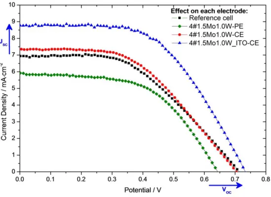
The effect of conductive lines on each electrode (photo and counter-electrodes) was studied for a device with 2 × 2 cm2 incorporating 4#1.5Mo1.0W metal lines. Fig. 6 shows that adding conductive lines to the photoelectrode lowers the conversion efficiency from 2.38 % to 2.09 %. Conversely, while adding the same lines to the counter-electrode enhances the conversion efficiency to 2.52 %. Table 6 shows that the applied Mo/W lines to the photoelectrode decrease both JSC and VOC, whereas when these lines are applied to the counter-electrode JSC increases and
VOC remains approximately constant. Furthermore, device 4#1.5Mo1.0W_ITO-CE with metal lines covered with a thin layer of indium-tin oxide (ITO) in the counter-electrode is discussed below.
Fig. 6 I-V characteristics for a DSC with a 2×2 cm2 design without lines (Reference cell) and the effect of adding
Mo/W lines on the photo and on the counter-electrode side.
Table 6 I-V parameters for a DSC with a 2×2 cm2 design without lines (Reference cell) and the effect of adding
Mo/W lines on the photo and on the counter-electrode side.
Device Active area / cm 2 VOC / V JSC / mA∙cm2 FF η / % Reference cell 4.0 0.71 6.93 0.48 2.38 4#1.5Mo1.0W-PE 3.5 0.64 5.92 0.55 2.09 4#1.5Mo1.0W-CE 4.0 0.70 7.35 0.49 2.52 4#1.5Mo1.0W_ITO-CE 4.0 0.73 8.78 0.55 3.53
The electrochemical impedance spectra obtained in the dark at applied potentials between 0.2 V and 0.7 V, with steps of 0.05 V, were fitted using a transmission line model and a simple circuit model, depending on the potential range [27]. Fig. 7 presents the resistance parameters as a function of the potential obtained from fitting the model to the Nyquist plot, where RS is the series resistance for the transport resistance of the TCO/lines, Rk is the charge-transfer resistance related to recombination of electrons at TiO2/electrolyte interface and Rw is the electron transport resistance in the mesoporous TiO2 photoelectrode.
Fig. 7 Fitted EIS parameters of the used electrical analogue circuit [27] as a function of applied potential for a 2 × 2 cm2 DSC cell with metal lines at the PE, CE and CE protected with ITO layer. A: series resistance (R
S) B:
recombination resistance (Rk) and C: transport resistance (Rw).
Compared with reference cell (ca. 7 Ω), the series resistance decreases for all devices with Mo/W lines, where the lowest value of 3.41 Ω is obtained for 4#1.5Mo1.0W_ITO-CE device. The recombination resistance (Rk) for 4#1.5Mo1.0W-PE device is smaller than for the reference cell; this is in agreement with the photovoltaic performance – Fig. 7. Moreover, this same device has a lower transport resistance (Rw), indicating that using conductive lines benefits the electron transport in the photoelectrode side. For the latter device, the electron recombination effect overcomes the electron transport resistance decrease induced by the Mo/W lines. The electron recombination increase should be related to the electrolyte reduction at the metal lines [28, 29]. On the other hand, 4#1.5Mo1.0W-CE device displays Rk and Rw values in line with the reference cell.
Since the use of collecting metal lines seems to increase the recombination rate, it was considered the use of a protective layer of ITO applied on the counter-electrode over the metal lines. ITO was selected since it is widely used on photovoltaic devices as DSCs due to its low sheet resistance and high transmittance in the visible region [30, 31]. However, this material is sensitive to the TiCl4 solution used to prepare the blocking layer at the photoelectrode side, preventing its use in the photoelectrode [32]. ITO layer was applied by magnetron sputtering up to a thickness of ca. 40 nm (4#1.5Mo1.0W_ITO-CE device). Sheet resistance measurements of this sample showed 2.63 Ω·□- 1, a value similar to that obtained for the best samples listed in Table 3. The results in
Fig. 7 and Table 6 indicates that the use of an ITO protective layer results in a substantial energy conversion efficiency increase, from 2.38 % to 3.53 %. Since all parameters controlling the efficiency and related to the photoelectrode are similar to device 4#1.5Mo1.0W-CE, the enhanced photovoltaic performance should be assigned to the counter-electrode as discussed below.
Half-cells of 2 × 2 cm2 were assembled in order to better understand the phenomena taking place in the counter-electrode side. The influence of adding 4#1.5Mo1.0W metal lines to a TCO glass substrate was analyzed. Also the effect of coating these lines with a ca. 40 nm thick ITO thin protective layer was assessed. All these devices were coated with a catalytic platinum layer sintered at 450 ºC. Fig. 8 displays the Nyquist plots of the three half-cells at 0 V.
Fig. 8 Half-cells assembled with counter-electrodes studied in this work. EIS spectra with Nyquist plots, for different substrates applied on the counter-electrodes in large-area 2 × 2 cm2 DSC devices. .
A simplified Randles electrical analogue was used to fit the experimental data as described elsewhere [33]. When Mo/W lines were added to the TCO glass substrate, the series resistance
(RS) decreased from 6.1 Ω to 2.2 Ω but the charge-transfer resistance at the counter-electrode (RCE) increased almost 8-fold, from 5.1 Ω to 39.5 Ω. Although Mo/W lines prejudices the counter-electrode performance in RCE, the device photovoltaic performance was increased due to the lower
RS. When adding the ITO protective layer RS was further reduced to 1.3 Ω and concomitantly RCE decreased to values close to that of the reference device, hence justifying the increased photovoltaic performance from the 4#1.5Mo1.0W_ITO-CE device.
4. Conclusions
The present work studied the use of metal lines on TCO glass substrates for minimizing the sheet resistance in large sized dye-sensitized solar cells. Though tungsten proved to be a promising metal for serving as current collector in DSCs, due to its chemical stability and high electrical conductivity, it proved to be quite difficult to sputter tungsten to the required line thickness. A bilayer collecting lines structure comprising of a bottom molybdenum layer capped with tungsten was optimised. The best performing design comprehends a 1.0 µm layer of W that coats a 1.5 µm layer of Mo. This design displays a good adhesion to the TCO layer and a lower sheet resistance. When ten metal lines were applied to 36 cm2 active area DSC, the sheet resistance decreased from 7 Ω·□-1 to 2.52 Ω·□-1 and the power conversion efficiency increased from 0.54 % (reference device) to 1.62 %. When these metal lines were applied to the photoelectrode the recombination rate resistance increased substantially, resulting in low performing DSC devices. A new approach was subsequently followed by coating the metal lines at the CE with a protective ITO layer; the DSC devices prepared this way improved the energy conversion efficiency to 3.53 %, by far overcoming the previous performances. Half-cells confirmed that the ITO protective layer shows significantly lower charge-transfer resistance compared with the substrate with bare metal lines.
Acknowledgements
A. I. Pereira is grateful to Portuguese Foundation for Science and Technology (FCT) through the project SolarConcept (PTDC/EQU-EQU/120064/2010). A. Mendes and L. Andrade acknowledge the European Commission through the Seventh Framework Programme, the Specific Programme "Ideas" of the European Research Council for research and technological development as part of an Advanced Grant under grant agreement no. 321315 (BI-DSC).
This work was also partially supported by the projects POCI-01-0145-FEDER-006939 (Laboratory for Process Engineering, Environment, Biotechnology and Energy – UID/EQU/00511/2013) funded by the European Regional Development Fund (ERDF), through COMPETE2020 - Programa Operacional Competitividade e Internacionalização (POCI) and by national funds, through FCT and by NORTE‐ 01‐ 0145‐ FEDER‐ 000005 – LEPABE-2-ECO-INNOVATION, supported by North Portugal Regional Operational Programme (NORTE 2020), under the Portugal 2020 Partnership Agreement, through the European Regional Development Fund (ERDF).
The authors are thankful to CEMUP for the SEM-EDS analysis and also to SEMAT/UM for the X-ray diffraction analysis.
References
[1] H. Ossenbrink, T. Huld, A. J. Waldau, and N. Taylor, "Photovoltaic Electricity Cost Maps," JRC Scienctific and Policy Reports, 2013.
[2] M. Gratzel, "Photoelectrochemical cells," Nature, vol. 414, pp. 338-44, Nov 15 2001. [3] K. Kakiage, Y. Aoyama, T. Yano, K. Oya, J. Fujisawa, and M. Hanaya, "Highly-efficient
dye-sensitized solar cells with collaborative sensitization by silyl-anchor and carboxy-anchor dyes," Chem Commun (Camb), vol. 51, pp. 15894-7, Nov 14 2015.
[4] M. A. Green, K. Emery, Y. Hishikawa, W. Warta, E. D. Dunlop, D. H. Levi, et al., "Solar cell efficiency tables (version 49)," Progress in Photovoltaics: Research and
Applications, vol. 25, pp. 3-13, 2017.
[5] L. Han, N. Koide, Y. Chiba, A. Islam, R. Komiya, N. Fuke, et al., "Improvement of efficiency of dye-sensitized solar cells by reduction of internal resistance," Applied
Physics Letters, vol. 86, p. 213501, 2005.
[6] J. Halme, P. Vahermaa, K. Miettunen, and P. Lund, "Device physics of dye solar cells,"
Adv Mater, vol. 22, pp. E210-34, Sep 15 2010.
[7] A. Fakharuddin, I. Ahmed, Q. Wali, Z. bin Khalidin, M. M. Yosuff, and J. Rajan, "Probing Electron Lifetime and Recombination Dynamics in Large Area Dye-Sensitized Solar Cells by Electrochemical Impedance Spectroscopy," Micro/Nano Science and
Engineering, vol. 925, pp. 553-558, 2014.
[8] A. Fakharuddin, P. S. Archana, Z. Kalidin, M. M. Yusoff, and R. Jose, "Standardization of photoelectrode area of dye-sensitized solar cells," Rsc Advances, vol. 3, pp. 2683-2689, 2013.
[9] K. Okada, H. Matsui, T. Kawashima, T. Ezure, and N. Tanabe, "100 mm x 100 mm large-sized dye sensitized solar cells," Journal of Photochemistry and Photobiology
a-Chemistry, vol. 164, pp. 193-198, Jun 1 2004.
[10] Z. Lan, J. H. Wu, J. M. Lin, and M. L. Huang, "Bi-functional TiO2 cemented Ag grid under layer for enhancing the photovoltaic performance of a large-area dye-sensitized solar cell," Electrochimica Acta, vol. 62, pp. 313-318, Feb 15 2012.
[11] G. R. A. Kumara, S. Kawasaki, P. V. V. Jayaweera, E. V. A. Premalal, and S. Kaneko, "Large area dye-sensitized solar cells with titanium based counter electrode," Thin Solid
Films, vol. 520, pp. 4119-4121, 2012.
[12] D. H. Yeon, K. K. Kim, N. G. Park, and Y. S. Cho, "Bismuth Borosilicate-Based Thick Film Passivation of Ag Grid for Large-Area Dye-Sensitized Solar Cells," Journal of the
American Ceramic Society, vol. 93, pp. 1554-1556, Jun 2010.
[13] J. Wu, Y. Xiao, Q. Tang, G. Yue, J. Lin, M. Huang, et al., "A large-area light-weight dye-sensitized solar cell based on all titanium substrates with an efficiency of 6.69% outdoors," Adv Mater, vol. 24, pp. 1884-8, Apr 10 2012.
[14] J. Chua, N. Mathews, J. R. Jennings, G. Yang, Q. Wang, and S. G. Mhaisalkar, "Patterned 3-dimensional metal grid electrodes as alternative electron collectors in dye-sensitized solar cells," Phys Chem Chem Phys, vol. 13, pp. 19314-7, Nov 21 2011.
[15] L. Meng, M. Wu, Y. Wang, W. Guo, C. Ma, T. Ma, et al., "Effect of the compact Ti layer on the efficiency of dye-sensitized solar cells assembled using stainless steel sheets,"
Applied Surface Science, vol. 275, pp. 222-226, 6/15/ 2013.
[16] G. J. Reynolds, T. M. Watson, G. Williams, and D. A. Worsley, "Corrosion Resistance of Metallic Substrates for the Fabrication Dye-Sensitized Solar Cells," Photovoltaics for
the 21st Century 6, vol. 33, pp. 129-138, March 21, 2011 2011.
[17] T. Watson, G. Reynolds, D. Wragg, G. Williams, and D. Worsley, "Corrosion Monitoring of Flexible Metallic Substrates for Dye-Sensitized Solar Cells," International Journal of
Photoenergy, vol. 2013, p. 8, 2013.
[18] J. Macaira, I. Mesquita, L. Andrade, and A. Mendes, "Role of temperature in the recombination reaction on dye-sensitized solar cells," Phys Chem Chem Phys, vol. 17, pp. 22699-710, Sep 21 2015.
[19] R. Cruz, D. A. P. Tanaka, and A. Mendes, "Reduced graphene oxide films as transparent counter-electrodes for dye-sensitized solar cells," Solar Energy, vol. 86, pp. 716-724, Feb 2012.
[20] E. Vassallo, R. Caniello, M. Canetti, D. Dellasega, and M. Passoni, "Microstructural characterisation of tungsten coatings deposited using plasma sputtering on Si substrates,"
Thin Solid Films, vol. 558, pp. 189-193, 2014.
[21] B. Girault, D. Eyidi, P. Goudeau, T. Sauvage, P. Guerin, E. Le Bourhis, et al., "Controlled nanostructuration of polycrystalline tungsten thin films," Journal of Applied Physics, vol. 113, p. 174310, May 7 2013.
[22] T. Karabacak, C. R. Picu, J. J. Senkevich, G. C. Wang, and T. M. Lu, "Stress reduction in tungsten films using nanostructured compliant layers," Journal of Applied Physics, vol. 96, pp. 5740-5746, Nov 15 2004.
[23] I.-L. Velicu, V. Tiron, C. Porosnicu, I. Burducea, N. Lupu, G. Stoian, et al., "Enhanced properties of tungsten thin films deposited with a novel HiPIMS approach," Applied
Surface Science.
[24] Y. G. Shen, Y. W. Mai, Q. C. Zhang, D. R. McKenzie, W. D. McFall, and W. E. McBride, "Residual stress, microstructure, and structure of tungsten thin films deposited by magnetron sputtering," Journal of Applied Physics, vol. 87, p. 177, 2000.
[25] L. J. v. d. Pauw, "A method of measuring specific resistivity and hall effect of discs of arbitrary shape," Philips Research Reports, vol. 13, pp. 1-9, 1958.
[26] S.-I. Jun, P. D. Rack, T. E. McKnight, A. V. Melechko, and M. L. Simpson, "Electrical and microstructural characterization of molybdenum tungsten electrodes using a combinatorial thin film sputtering technique," Journal of Applied Physics, vol. 97, p. 054906, 2005.
[27] F. Fabregat-Santiago, J. Bisquert, G. Garcia-Belmonte, G. Boschloo, and A. Hagfeldt, "Influence of electrolyte in transport and recombination in dye-sensitized solar cells studied by impedance spectroscopy," Solar Energy Materials and Solar Cells, vol. 87, pp. 117-131, 2005.
[28] S. Ito, P. Liska, P. Comte, R. Charvet, P. Pechy, U. Bach, et al., "Control of dark current in photoelectrochemical (TiO2/I--I3-) and dye-sensitized solar cells," Chemical
Communications, pp. 4351-4353, 2005.
[29] H. Zheng, Y. Tachibana, and K. Kalantar-Zadeh, "Dye-sensitized solar cells based on WO3," Langmuir, vol. 26, pp. 19148-52, Dec 21 2010.
[30] K. Goto, T. Kawashima, and N. Tanabe, "Heat-resisting TCO films for PV cells," Solar
Energy Materials and Solar Cells, vol. 90, pp. 3251-3260, 2006.
[31] K.-S. Tseng and Y.-L. Lo, "Effect of sputtering parameters on optical and electrical properties of ITO films on PET substrates," Applied Surface Science, vol. 285, Part B, pp. 157-166, 11/15/ 2013.
[32] S. Gardonio, L. Gregoratti, D. Scaini, C. Castellarin-Cudia, P. Dudin, P. Melpignano, et
al., "Characterization of indium tin oxide surfaces after KOH and HCl treatments," Organic Electronics, vol. 9, pp. 253-261, 2008.
[33] A. Hauch and A. Georg, "Diffusion in the electrolyte and charge-transfer reaction at the platinum electrode in dye-sensitized solar cells," Electrochimica Acta, vol. 46, pp. 3457-3466, 2001.


![Fig. 7 Fitted EIS parameters of the used electrical analogue circuit [27] as a function of applied potential for a 2 × 2 cm 2 DSC cell with metal lines at the PE, CE and CE protected with ITO layer](https://thumb-eu.123doks.com/thumbv2/123dok_br/15725420.1070928/15.892.135.759.110.318/fitted-parameters-electrical-analogue-circuit-function-potential-protected.webp)
