ISSN 1517-7076 artigo e-11963, 2018
Corresponding Author: Kitsakorn Locharoenrat Received on: 15/11/2016 Accepted on: 27/11/2017
10.1590/S1517-707620170001.0299
Improvement of power efficiency of hybrid
white OLEDs based on p-i-n structures
Apisit Chittawanij1, Kitsakorn Locharoenrat1
1Department of Physics, Faculty of Science, King Mongkut’s Institute of Technology Ladkrabang, Bangkok 10520, Tha i-land
e-mail: [email protected], [email protected]
ABSTRACT
In this article, hybrid white organic light-emitting diodes (WOLEDs) under p-i-n structures have been investigated in terms of power efficiency. By using tris(8-hydroxy quinolinato) aluminum (Alq3) doped with 8-hydroxy-quinolinato lithium (Liq) as an n-type and WHI112 doped with molybdenum trioxide (MoO3) as a p-type, the typical device structure of ITO/WHI112: 20 wt.% MoO3 (55 nm)/HTG-1 (10 nm)/UBH15: 3 wt.% EB502 (10 nm)/EPH31: 3 wt.% EPY01 (25nm)/3TPYMB (10 nm)/Alq3: 33 wt.% Liq (25 nm)/Al (150 nm) was fabricated. It has been found that the p-i-n device based device showed the lowest driving voltage and highest power efficiency among the undoped and n-type devices. At the current density of 20 mA/cm2, the roll-off of the efficiency in the p-i-n device was much smaller than the n-type and the undoped devices. The current and power efficiency of the p-i-n device were maintained with 17.2 cd/A and 5.1 lm/W at 100 mA/cm2, it was reduced to 7.5 % and 21 %, respectively. In contrast, the n-type device exhibited the significant reduction of efficiency (14.4 cd/A and 3.8 lm/W at 80 mA/cm2), it was reduced to 20 % and 39.6 %, respectively. The superior performances of the p-i-n structure based device were attributed to the high hole injection ability of WHI112:MoO3 and high electron mobility of Alq3:Liq, leading to high power efficiency and low driving voltage. A better balance of electrons and holes could contribute to a good current efficiency for the device. These findings strongly indicated that carrier injection ability and balance showed significant affects on the performance of OLED.
Keywords: Highly efficient OLEDs, hybrid white OLEDs, p-i-n OLED.
1. INTRODUCTION
the ITO/HTL interface. Judicious control of doping levels can also lead to the efficient carrier injection by the tunneling [16]. It is very difficult to balance the holes and electrons in the emitting layer, because hole mobility is generally faster than the electron mobility in organic materials. In order to solve this problem, several kinds of HTL, ETL, hole block layer and electron block layer have been studied [17,18].
In this paper, we have demonstrated hybrid white organic light-emitting diode (WOLEDs) devices based on the p-i-n structure with Liq doped into Alq3 as the n-doping layer and MoO3 doped into WHI112 as the p-doping layer. In order to reduce the driving voltage and improve efficiency, we use MoO3 doped into WHI112 as the p-doping layer and Liq doped into Alq3 as the n-doping layer, power efficiency and carrier balance have been overwhelmingly improved. The electrical engineering and hybrid WOLED charge balance are developed based on these experimental results. The mechanism of such improvement is also discussed on these experimental results.
2. MATERIALS AND METHODS
Glass coated with indium-tin oxide (ITO) was used as the starting substrate. The substrate was immersed sequentially in acetone and isopropyl alcohol under the ultrasonic bath for 15 min each, following by rinsing in DI water. The substrates were dried with nitrogen gas. Then the samples were treated with the oxygen plasma for 1 min. prior to use. The devices were prepared by the vapor deposition onto the ITO coated glass substrate. Firstly, the series of electron-only devices were fabricated in order to obtain some data on the electron transport ability of Alq3 doped with Liq layers. The structures of electron-only devices were as follows: ITO/Alq3: x wt.% Liq (30 nm)/Al (130 nm), where x was 0 wt.% for device E-1, 10 wt.% for device E-2, 33 wt.% for device E-3, and 50 wt.% device E-4 (Table 1). Secondly, the study of hole-injection ability of WHI112 doped with MoO3 layer, the series of hole-only devices were fabricated. Hole-only device got the following structures: ITO/ WHI112: y wt% MoO3 (50 nm)/ HTG-1 (15 nm)/Al (130 nm), y was 0 wt.% for device H-1, 10 wt.% for device H-2, 20 wt.% for device H-3, and 30 wt.% for device H-4 (Table 2).
Table 1: The parameters of electron-only devices.
DEVICE
ANODE n-TYPE CATHODE
Alq3 Liq Al
E-1 ITO 30 nm 0% 130 nm
E-2 ITO 30 nm 10% 130 nm
E-3 ITO 30 nm 33% 130 nm
E-4 ITO 30 nm 50% 130 nm
Table 2: The parameters of hole-only devices.
DEVICE ANODE p-TYPE HTL CATHODE
WHI112 MoO3 HTG-1 Al
H-1 ITO 50 nm 0% 15 nm 130 nm
H-2 ITO 50 nm 10% 15 nm 130 nm
H-3 ITO 50 nm 20% 15 nm 130 nm
H-4 ITO 50 nm 30% 15 nm 130 nm
the cathode layer were deposited under the ultrahigh vacuum chamber at 4x10⁻⁶ Torr. The active area of the devices was 5x5 mm2. The thickness of the organic layers was monitored by using quartz-crystal monitor. Current-voltage characteristics were measured with the computer-controlled Keithley 2400 Source Meter and elctroluminescence (EL) spectra was measured with the Spectrascan PR650 photometer. All the measurements were carried out at room temperature and atmosphere.
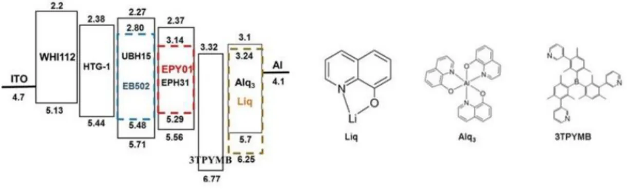
Figure 1: Energy band diagrams and molecular structures of the tested materials.
Table 3: The parameters of undoped, n-doped and p-i-n devices.
DEVICE HIL
p-DOPANT HTL BLUE EML YELLOW EML HBL ETL
n-DOPANT EIL
WH112 MoO3 HTG-1 UBH15 EB502 EPH31 EPY01 3TPYMB Alq3 Liq LiF undoped
55 nm
-
15 nm
- 0.8 nm
n-doped - 10 nm 3% 25% 3% 10nm 25 nm
33% -
p-i-n 20%
3. RESULTS AND DISCUSSION
3.1 Characteristics of electron-only and hole-only devices
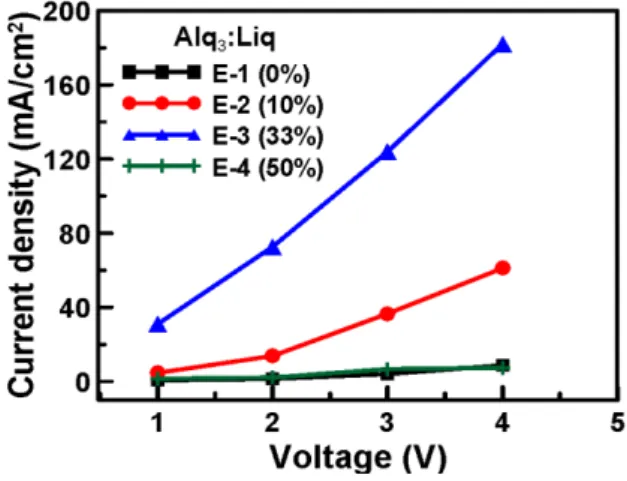
In electron-only device, the current density as a function of voltage (J-V) characteristics at the various Liq doped into Alq3ratios are shown in Fig. 2. In electron-only device, a rapid increasing in the device current occurs when Liq is doped into the Alq3 layer. Increasing the current density is seen when a small 10 wt.% Liq doping concentration is introduced into the Alq3 layer, as compared with the control device. The J-V charac-teristics of electron-only device are strongly dependent on the doping ratio in the electron transport layer. At the same voltage, the current density increases along with increasing the doping ratio. The highest current density is observed at 33 wt.% Liq doping ratio. The E-1, E-2, E-3 and E-4 device driving voltage at 100 mA/cm2 are 8, 5.3, 2.6 and 6.7 V, respectively. These electron-only device J-V characteristics suggest that a certain Liq to Alq3doping ratio could improve the co-deposited layer electron transport ability. The advantage of using Alq3:Liq as the ETL is explained using the electron hopping exchange along with their Lowest Un-occupied Molecular Orbital (LUMO). In a single host device, electrons hop along the LUMO in Alq3. Since the LUMO-LUMO difference between Alq3 (3.1eV) and Liq (3.24 eV) is negligible, subject to their similar LUMO, transport manifolds alongwith their LUMO are expected to exhibit a certain extent of overlapping after a mixing ratio goes beyond 33 wt.% Liq. Therefore, it is likely that a large energetic disorder between Alq3 and Liq contributes to the electron hopping, implying that electron hopping among Alq3 and Liq sites is favorable[19]. The high electron conductivity of Alq3:Liq might originate from the short electron transport hopping length as compared with the pure Alq3 ETL. However, the current conduction is reduced dramati-cally as the doping ratio is further increased to 50 wt.% in the device E-4. This result is attributed to the car-rier quenching and defection effects.
Comparing with the undoped device, we could see that the low doping strikingly decreases the driving voltage and the J-V characteristics are strongly dependent on the hole injection layer doping ratio. At the same voltage, the current density increases along with increasing MoO3 doping ratio. The highest current density is observed at 20 wt.% MoO3 doping ratio, indicating that the p-doping HIL layer conductivity increases due to MoO3 doping into WHI112. The H-1, H-2, H-3 and H-4 device driving voltages are 5.4, 4.3, 3.8 and 4.2 V, respectively. The results indicate that doping MoO3 reduces the potential barrier for the hole injection at the ITO interface [20]. The hole-only device current enhancement is attributed to the reduction of resistivity and activation energy, leading to decreased ohmic losses.
Figure 2: Electron-only J-V characteristics of devices E-1 to E-4.
Figure 3: Hole-only J-V characteristics of devices H-1 to H-4.
It is possible that the high holes are transferred from the Highest Occupied Molecular Orbitals (HO-MO) in the WHI112:MoO3 matrix into the HTG-1 HOMO. The MoO3 (5.3 eV) and HTG-1 (5.4 eV) HOMO levels have closely energetic positions making a charge transfer and energetically favorable process. The hole transfer results in increased charge carrier concentration in the bulk HTL which increases the film conducti-vity and reduces HTL ohmic losses during the device operation. Through the increased bulk conducticonducti-vity process, the current density is expected to increase with increasing the doping concentration. However, our devices demonstrate the reduced performance at higher 20% MoO3 to WHI112 concentration. It is likely that because the heavy doping MoO3 molecules saturate the layer and escape into the HIL (WHI112:MoO3)/HTL (HTG-1) interface. This thin MoO3 layer creates a dipole barrier at the interface with HTL which increases the necessary device driving voltage. It is possible that a high MoO3 concentration might lead to significant dopant diffusion through the HTL into the EML, causing electroluminescence (EL) quenching in the emissi-ve region. This suggests that the aggregations tend to degrade the device performance.
3.2 Comparison between undoped and n-type devices of hybrid WOLEDs
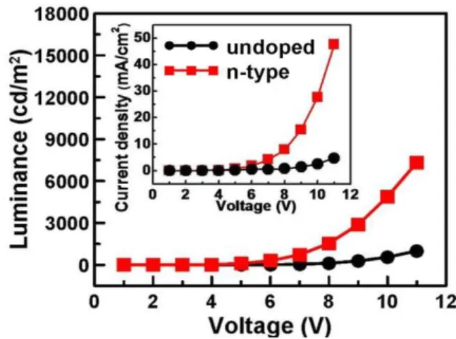
solid-state lighting sources. The yellow phosphorescent with the blue fluorescent emitter combination might result in a good compromising among the high efficiency hybrid systems. We know that in conventional de-vices, such as undoped device, the number of the holes is much greater than the number of the electrons. A surplus of the holes at the HTL/EML interface increases the probability that EML cations are formed, leading to the device degradation rapidly. From the electron-only device, the further experiments should focus on a device with Alq3: 33 wt.% Liq layer as the n-doping. The n-type device with 33 wt.% Liq doped into Alq3 as the electron carrier for hybrid WHOLEDs is therefore studied. It is very important to balance out the current supply to the emission zone. This is carried out with 3TPYMB as the electron-blocking and HTG-1 as hole-blocking layers nearby the emission zone. These layers create an additional barrier for the carriers to be injec-ted. The result shows that the recombination and/or emission zone is clearly separated from the area with the high carrier concentration. The structure of this device is ITO/WHI112 (55 nm)/HTG-1 (10 nm)/UBH15: 3 wt.% EB502 (10 nm)/EPH31: 3 wt.% EPY01 (25nm)/3TPYMB (10 nm)/Alq3: 0 or 33 wt.% Liq (25 nm)/with or without LiF (0.8 nm)/Al (150 nm), where Liq is 0% with LiF for undoped device and Liq is 33 wt.% without LiF for n-type device. Figure 4 shows L-V and J-V (inset) characteristics of undoped and n-type devices.The n-type device shows the lower operational voltage and higher current density and luminance slopes than the undoped device. It is clearly seen that under the same current density, the n-type device pro-duces higher emissions than the undoped device. This represents the lower electron injection barrier and higher efficiency from the n-type device. Therefore Alq3:Liq produces the higher electron injection efficiency and higher luminance than LiF. The power efficiency of the two devices is shown in Fig. 5. The power effici-encies of the undoped and n-type devices are 6.4 and 7.81 lm/W at 5 mA/cm2, respectively. The driving vol-tage of the n-type device at 5 mA/cm2 is 7.2 V, which is reduced, as compared with the undoped device (11 V). This significant enhancement of performance is attributed to the improved transport conductivity of the n-doping Liq doped into Alq3layer. This shows that Liq incorporation into Alq3 materials could improve de-vice performance, by increasing the electron concentration in Alq3 films and moving the Fermi level close to the LUMO of Alq3 [19].
Figure 5: Power efficiency-current density characteristics of undoped and n-type devices.
3.3 Comparison between n-typeand p-i-n devices of hybrid WOLEDs
The power efficiency depends on the carrier injection, the transportation and the carrier balance. The p-i-n device is fabricated in which the WH112 layer is doped with 20 wt.% MoO3 in the ITO/WHI112: 20 wt.% MoO3 (55 nm)/HTG-1 (10 nm)/UBH15: 3 wt.% EB502 (10 nm)/EPH31: 3 wt.% EPY01 (25nm) Alq3: 33 wt.% Liq (25 nm)/Al (150 nm) configuration. The n-type device and p-i-n device characteristics are displa-yed in Figs. 6-8.
Figure 7: Power efficiency-current density character-istics of hybrid WOLEDs of n-type and p-i-n devices.
Figure 8: Electroluminescence (EL) spectra of hybrid WOLEDs of n-type and p-i-n devices.
As compared with the n-type device, the L-V and J-V (inset) curves of the p-i-n device are significan-tly enhanced, indicating that the device conductivity is improved using the p-i-n structure, as shown in Fig. 6. It is clear that the power efficiency of the p-i-n device is considerably increased as compared with the n-type device as shown in Fig. 7. This indicates the improvement of the p-i-n deviceconductivity. Table 4 summari-zes the data for both devices obtained from the n-type device and p-i-n device at 20 mA/cm2. The p-i-n devi-ce current efficiency, power efficiency and voltage are improved at 18.6 cd/A, 6.5 lm/W and 8.9 V at 20 mA/cm2, respectively, as compared with the n-type device at 18 cd/A, 6.3 lm/W and 9.4 V, respectively.
Table 4: Performance of hybrid WOLED devices at 20 mA/cm2.
DEVICES VOLTAGE LUMINANCE YIELD POWER EFFICIENCY CIE (X,Y)
n-type 9.4 V 3600 cd/m2 18.0 cd/A 6.3 lm/W 0.45,0.50
p-i-n 8.9 V 3720 cd/m2 18.6 cd/A 6.5 lm/W 0.39,0.48
WHI112 and the electron-transport property of 33 wt.% Liq doped into Alq3 is contributed to the controlling the holes and the electrons in the light-emitting layer and results in the stable efficiency roll-off hybrid WOLED. Figure 8 shows the EL spectra of the n-type device and p-i-n device. The EL spectrum shows the difference of the peak between these two devices. It is interesting to note that the EL spectrum of the p-i-n device is high as compared with the n-type device. The blue peak spectrum appeared as the electron injection is increased and it shifts the recombination into the blue emission layer. This indicates that the p-i-n device plays a major impact on the hybrid WOLED optical characteristics. The CIE coordinates of the n-typeand p-i-n devices are (0.45, 0.50) and (0.39, 0.48), respectively, as shown in Table 1. As the result, the p-p-i-n device contributes to a certain degree to the good hole-electron balance in the light-emitting layer.
4. CONCLUSIONS
We have presented the hybrid WOLEDs based onp-i-n structure of novel Alq3:Liq and WHI112:MoO3 as n-type and p-n-type, respectively. Current efficiency of 18.6 cd/A, power efficiency of 6.5 lm/W, and driving voltage 8.9 V at a current density of 20 mA/cm2 in p-i-n hybrid WOLEDs were obtained. The roll-off of the efficiency in the p-i-n device was much smaller than the n-type and undoped devices. The current and power efficiency of the p-i-n device were maintained with 17.2 cd/A and 5.1 lm/W at 100 mA/cm2, it was reduced to 7.5 % and 21 %, respectively. In contrast, the n-type device exhibited the significant reduction of the effi-ciency (14.4 cd/A and 3.8 lm/W at 80 mA/cm2), it was reduced to 20 % and 39.6 %, respectively. The supe-rior performance was attributed to the high hole and electron ability of WH112:MoO3 and Alq3:Liq, leading to low driving voltage and better electron and hole balance, contributing to enhanced efficiency even at the high current density. Effective carrier balance between the holes and electrons was achieved from the en-hanced transport layer conductivity, leading to the device enen-hanced efficiency.
5. ACKNOWLEDGMENTS
This work is supported by King Mongkut’s Institute of Technology Ladkrabang (KREF145901).
6. BIBLIOGRAPHY
[1] LEE, K.S., LIM, I.S., HAN, S.H., et al., “Enhancement of the power efficiency for p-i-n OLEDs contain-ing organic p-type HAT-CN and n-type LCV materials”, Organic Electronics, v. 15, n.2, pp. 343-347, Feb. 2014.
[2] YANG, J.P., BAO, Q.Y., XIAO, Y., et al., “Hybrid intermediate connector for tandem OLEDs with the combination of MoO3-based interlayer and p-type doping”, Organic Electronics, v.13, n.1, pp. 2243-2249, Nov. 2012.
[3] XIE, G.H., FEHSE, K., LEO, K,, et al., “Novel P-I-N-P top-emitting organic light-emitting diodes with enhanced efficiency and stability”,Organic Electronics, v. 14, pp. 2331-2340, Sep. 2013.
[4] LEE, J.H., KIM, J.W., KIM, S.Y., et al., “An organic p–n junction as an efficient and cathode independ-ent electron injection layer for flexible inverted organic light emitting diodes”, Organic Electronics, v. 13, pp. 545-549, Sep. 2012.
[5] DING, L., ZHANG, F., MA, Y., et al., “Aluminum/MoO3 anode thin films: an effective anode structure for high-performance flexible organic optoelectronics”, Journal of Semiconductors, v. 33, pp. 013003-1-4, Jan. 2012.
[6] MEYER,J., KIDAMBI, P.R., BAYER, B.C., et al., “Metal oxide induced charge transfer doping and band alignment of graphene electrodes for efficient organic light emitting diodes”, Scientific Reports 4, n. 5380, pp. 1-7, Jun. 2014.
[7] ZHANG,X., YOU, F., ZHENG, Q., et al., “Solution-processed MoOx hole injection layer towards effi-cient organic light-emitting diode”, Organic Electronics, v. 39 pp. 43-49, Sep.2016.
[8] HUH, Y.H., KWON, O.E., PARK, B., “Triple-stacked hole-selective layers for efficient solution-processable organic semiconducting devices”, Optics Express, v. 23, n.11, pp. A625-A639, May 2015. [9] NIKIFOROV, G.O. “Molecular p doping of 4,40-Bis(N-carbazolyl)-1,10-biphenyl and n doping of 1,3,5-tris(N-phenylbenzimidazol-2-yl)benzene”, Organic Electronics,v. 36, pp.120-132, Jun. 2016.
[10] LUSSEM, B., RIEDE, M., LEO, K. “Doping of organic semiconductors”, Physica Status Solidi A 210, v. 1, pp. 9-43, Dec. 2013.
high-efficiency and long-term stable tandem organic light-emitting diodes”, ACS Applied Materias &Interfaces, v. 6, n.20, pp. 18228-18232, Oct. 2014.
[12] TSANG, D.P.-K.,MATSUSHIMA, T., ADACHI, C., “Operational stability enhancement in organic light-emitting diodes with ultrathin Liq interlayers”, Scientific Reports. v. 6, p. 22463, Mar. 2016.
[13] ZHANG, L., ZU, F.-S., DENG Y.-L., et al., “Origin of enhanced hole injection in organic light-emitting diodes with an electron-acceptor doping layer: p-type doping or interfacial diffusion”, ACS Applied Materias & Interfaces, v. 7(22), pp. 11965-11971, May 2015.
[14] ZHANG, L., ZHOU, D.-Y., WANG, B., et al., “Enhanced efficiency and stability in organic light-emitting diodes by employing a p-i-n-p structure”, Applied Physics Letters, v.109, n.17, pp.173302-1-173302-4, Oct. 2016.
[15]WANG, B., ZHANG, L, HU, Y., et al., “Doped hole injection bilayers for solution processable blue phosphorescent organic light-emitting diodes”, Journal of. Materials Chemistry C, v. 4, pp. 6570-5674, Jun. 2016.
[16] GAO, J., NILES, E.T., GREY, J.K., Aggregates promote efficient charge transfer doping of poly(3-hexylthiophene), Journal of Physical Chemistry Letters, v. 4, n.17, pp. 2953-2957, Aug. 2013.
[17] MURANO, S., PAVICIC, D., FURNO, M., et al., “Outcoupling enhancement mechanism investigation on highly efficient PIN OLEDs using crystallizing evaporation processed organic outcoupling layers”, SID Symposium Digest of Technical Papers, v. 43, pp.687-690, Jun. 2012.
[18] ZHANG, D., DUAN, L., ZHANG, D., et al., “Extremely low driving voltage electrophosphorescent green organic light-emitting diodes based on a host material with small singlet–triplet exchange energy with-out p- or n-doping layer”, Organic Electronics, v. 14, n.1, pp. 260-266, Jan. 2013.
[19] KIM, S., CHOI, P., KIM, S., et al., “Analysis of the electrical properties of an electron injection layer in Alq3-based organic light emitting diodes”, Journal of Nanoscience and Nanotechnology, v. 16(5), pp. 4742-4745, May 2016.
[20] QIU, Y.J., High Efficiency Organic Light Emitting Diodes with MoO3 Doped Hole Transport Layer,