886 Brazilian Journal of Physics, vol. 36, no. 3B, September, 2006
Silicon Adsorption In Single Walled Nanotubes
M. L. Colussi∗, L.P. Neves+, and R.J. Baierle∗
∗1Departamento de F´ısica da UFSM, Faixa de Camobi Km 9, 97105-900, Santa Maria – RS, Brazil
+Centro Universit´ario Franciscano, Rua dos Andradas 1614, 97010-032, Santa Maria – RS, Brazil
Received on 8 December, 2005
Using density functional (DF) calculations and Monte Carlo (MC) simulations we have investigated the main electronic and structural properties of silicon interacting with single walled carbon nanotubes. We have inves-tigated the silicon adsorption externally and internally in the nanotubes surface. The total energies calculations and charge density plot present that the adsorption is most stable externally with silicon forming four bonds with the C atoms and the Si-C bond distances are similar to the ones in the SiC crystal. When silicon is adsorbed in a semiconductor nanotube, a new occupied electronic level inside the band gap is observed. For the metallic tube, the electronic silicon levels are close to the Fermi energy, increasing the metallic tube character.
Keywords: Nanotube; Silicon adsorption; Monte Carlo simulations; First principle calculation
I. INTRODUCTION
Carbon nanotubes (CNTs) were identified for the first time by S. Iijima in 1991 as by-products of arch discharge ex-periments[1]. They can be considered a new form of matter and are some of the first true nanomaterials engineered at the molecular level. They exhibit unique structural and electronic properties and can be considered quasi-one-dimensional ma-terials, with promising applications in nanometric devices[2]. The electronic and structural properties of single walled car-bon nanotubes (SWCNTs) have been theoretically studied [3] and confirmed experimentally [4]. The main electronic fea-tures can be understand using the hexagonal graphite network as guide[2]. Tubular graphitic forms of Si and Ge have been proposed [5], but no stable forms have yet being obtained. The difficulties for Si and Ge form hexagonal graphitic network can be associated with the considerable energies difference between the sp2and the sp3hybridization[6].
Silicon is the most important material in the microelectron-ics and the interaction between nanotubes and Si is a very im-portant subject that need to be clarified. The substitutional silicon doping in SWCNTs has been theoretically studied[7]. The formation energies are around 3.1 eV and the main elec-tronic feature is an unoccupied level inside the band gap for a semiconductor nanotube. The interaction between a tube and the clean Si(001) surface have been recently studied by Orel-lanaet al.[8]. They have shown that the nanotube adsorption (contact) by the silicon surface increases the density of states near the Fermi level, enhancing the metallic character of the nanotube.
In this work, using Monte Carlo (MC) simulations with a many-body empirical potential and first principle calculations, we have studied the adsorption of a Si atom internally and ex-ternally in two different nanotubes: the semiconductor zigzag (10,0) and the metallic armchair (6,6). In the next section we present the methodology used, in section three the results and discussion, and in section four our conclusions.
II. METHODOLOGY
Using empirical many-body potential with the Monte Carlo method [9], the binding energy is
Ebind=
∑
i∑
j>i
[VR(ri j)−Bi jVA(ri j)]
M. L. Colussi et al. 887
cutoff of 80 Ry to calculate the self consistent Hamiltonian matrix elements. To sampling the Brillouin zone (BZ) a set of three Morkhost-Pack special k-points [21], along the tube axis, has been used.
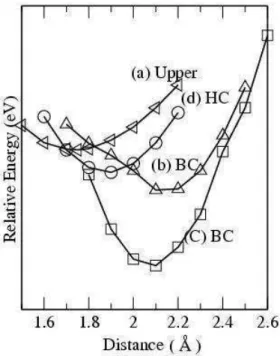
FIG. 1: Relative Energy for Si atom on a external surface in a (10,0) nanotube. In axis X the distances are in Angstroms and represent the Si-C distance when (a) the Si is adsorbed on the top of a C atom, (b-c) in the bond center for the two C-C possible bonds orientation (parallel or making 600with the tube axis) and (d) the distance from
the Si to a hexagon center.
Our study is performed using two tubes with different chi-ralities: the semiconductor (10,0) zigzag with 9.924 ˚A of di-ameter and the metallic (6,6) armchair with 10.312 ˚A of diam-eter. We use periodic boundary conditions with a tetragonal supercell with dimensions of 16 ˚A in directions perpendicu-lar to the tube axis and the translational symmetry along the tube axis. This construction should eliminated possible inter-tube interaction or inter adsorbed silicon atoms. The supercell for the (10,0) tube have 120 C atoms and for the (6,6) have 72 atoms, in each case we are using three conventional unit cells. All the atoms in the enlarged unit cell are relaxed. The forces are calculated using the Hellmann-Feymann procedure and the geometry are optimized using the Conjugated Gradi-ent scheme (CG). The system is relaxed until the root mean square criterion of 0.05 eV/ ˚A on the atomic force is reached.
In the first principle calculations, the binding energies of a given system are determined using total energies calculations, according to equation:
Eb=Et[tube+Si]−Et[tube]−Et[Si]
where Eband Etare the formation and total energies, respec-tively. Negatives values for the binding energy means that the adsorption is exothermic.
III. RESULTS AND DISCUSSION
Carbon nanotubes (CNTs) exhibit unique structural and electronic properties. For example zigzag (n,0), with n not being a multiple of 3, are semiconductor with a finite gap that depend only the tube diameter while the armchair (n,n) present a metallic behavior.
The gap and the density of states around the Fermi level for the CNTs are predicted to be dependent on the chemi-cal/physical adsorption of atoms and molecules by the tube wall. In this work we have studied the main electronic and structural properties when a silicon atom is adsorbed exter-nally and interexter-nally in SWCNTs.
Our empirical calculations are not able to detect energy dif-ferences between different tubes. For the two tubes studied we obtain that the cohesion energy per atom is 7.25 eV, these value is close to the cohesion energy per atom in the graphitic structure (7.4 eV) obtained using the same approach [10,11].
When silicon is adsorbed on the tube wall, we observed a preference for the external surface. For the (6,6) armchair, the binding energies are -1.51 eV and -0.47 eV for the external and internal surface, respectively. For the (10,0) zigzag these values are –1.41 eV and -0.32 eV.
In our ab initio calculations we studied the Si adsorption in three candidate sites: center of hexagon, on the top a C atom and in the bond center. Fig. 1 show the results obtained when the Si atom is approximated to the external tube surface in the (10,0) semiconductor tube, for the three candidates sites.
The most stable position, lower binding energy, for the three sites investigated is the bond center position where the silicon atom is connected with the C atoms by four bonds, as indicated in the Fig. 2. Results for the armchair and the in-ternal surface are similar. The calculated binding energy are –2.80 eV (external) and –2.46 eV (internal) and –2.61 (exter-nal) and –2.22 eV (inter(exter-nal) for the (10,0) and the (6,6) nan-otubes, respectively.
FIG. 2: Silicon adsorbed on the external surface in a (10,0) semicon-ductor nanotube. Part (a) is a lateral sight and part (b) is the top sight. The Si-C bond distance are 2.1 ˚A.
888 Brazilian Journal of Physics, vol. 36, no. 3B, September, 2006
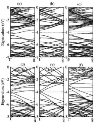
FIG. 3: Bands Structure for the (10,0) (a-c), and (6,6) (d-f) nanotubes when a Si atom is adsorbed in the tube wall. In parts (a) and (d) the Si is bonded on the externally and in parts (c) and (f) internally. Parts (b) and (e) are the bands structure for the “clean” surface. The dotted lines indicate the Fermi energy.
FIG. 4: Spatial localization of the charge density for the HOMO when a silicon atom is adsorbed in the external surface of a (10,0) carbon nanotube.
For the semiconductor (10,0) the appearance of the new electronic levels can be more clearly observed. For the ex-ternally (Fig.3-c) and inex-ternally (Fig 3-a) adsorption an occu-pied electronic level, the HOMO (highest occuoccu-pied molecular orbital) is present in the tube gap.
In figure 4 we can observe that the HOMO is localized on the foreign impurity (Si atom) and the C atoms that are bonded with the silicon. A similar charge density plot (not showed here) for the bottom of the conduction band show a weakly contribution from the Si atom. For the (6,6) nanotube the electronic levels near to the Fermi energy have a strong contribution from the Si atom, indicating that the adsorbed Si atom introduce localized states close to the Fermi energy in a metallic nanotube, enhanced the metallic character.
An analysis of the M¨ulliken population presents a charge transference from the nanotube to the silicon. For the (10,0) tube we obtain 0.176e(eis the fundamental electric charge) and 0.054e, for the internal and external surface, respectively. For the (6,6) tube the charge transferred is 0.024eand 0.194 e. The charge transference is in agreement with the binding energy results.
IV. CONCLUSIONS
In conclusion, our calculations for the binding energy present that Si is chemically adsorbed on the tube surface with a preference for the external surface (lower binding energy), that is confirmed by the charge density plot and the Mulliken population analysis. When the silicon is adsorbed in a semi-conductor (10,0) tube a new occupied electronic level will be present in the gap. For the metallic (6,6) tube we observe an increase in the density of states near the Fermi level, as consequence the tube metallic character is enhanced. The sil-icon adsorption is an exothermic reaction (negative binding energies) and it can be considered for the possibility to con-struct tubular forms of mixed SiC compounds[22]. However, the binding energies are lower than the Si cohesive energy in-dicating that in an Si-rich environment, the Si atoms should aggregated forming the Si crystalline (or cluster). When a sil-icon is substitutional in a SWCNT it is threefold coordinated and for the adsorbed silicon it is fourfold coordinated (in the most stable configuration) making the adsorbed silicon a non candidate for a reactive center. The chemical binding between the Si adsorbed by the tube surface and a foreign impurity (like H, O, OH, O2)must destroy the weak bond between the adsorbed Si and the tube wall.
Acknowledgement
This work was supported by Brazilian agencies CAPES and CNPq and FAPERGS. The calculations have been performed using the facilities of the Centro Nacional de Processamento de Alto Desempenho (CENAPAD in Campinas).
Prrop-M. L. Colussi et al. 889
erties of Carbon Nanotubes, London, World Scientific (1998). [3] R. Saito, M. Fujita, G. Dresselhaus, and M.S. Dresselhaus,
Appl. Phys. Lett.60, 2204 (1992).
[4] S.J. Tans, M.H. Devoret, H. Da´ı. A. Thess, R. E. Smalley, L.J. Geerligs, and C. Dekker, Nature386, 474 (1997).
[5] S.B. Fagan., R.J Baierle, R. Mota, A.J.R. da Silva, and A. Fazzio, Phys. Rev. B 61, 9994 (2000); G. Seifert, T. K¨ohler, H. M. Urbassek, E. Hernandez, and T. Frauenheim, Phys. Rev. B63, 193409 (2001); G. Seifert, T. K¨ohler, Z. Hajnal, and T. Frauenheim, Solid State Commun.119, 653 (2001).
[6] M.T. Yin and M.L. Cohen, Phys. Rev. B23, 5048 (1981). [7] R.J. Baierle, S.B. Fagan, R. Mota, A.J.R. da Silva, and A.
Fazzio, Phys. Rev. B64, 085413 (2001).
[8] W. Orellana, R.H. Miwa, and A. Fazzio, Phys. Rev Lett.91, 166802, (2003); W. Orrelana, R.H. Miwa, and A. Fazzio, Surf. Science,566, 728 (2004).
[9] J. M. Hammersley, D.C. Handscomb,Monte Carlo Methods, Wiley, New York, (1979).
[10] J. Tersoff, Phys. Rev. Lett.56, 632 (1986). [11] J. Tersoff, Phys. Rev. B37, 6991 (1998).
[12] D. H. Robertson, D.W. Brenner, J.W. Mintmire, Phys. Rev. B
45, 12592 (1992).
[13] N. Hamada, S. Sawada, A. Oshiyama, Phys. Rev. Lett.68, 1579 (1992).
[14] S. B. Fagan, R. Mota, R.J. Baierle, G. Paiva, A.J.R. da Silva, and A. Fazzio, J. of Molec. Sturcture539, 101 (2001). [15] D. M. Ceperley, B. Alder, J. Phys. Rev. Lett.45, 566 (1980). [16] J. P. Perdew, A. Zunger, Phys. Rev. B23, 5048 (1981). [17] P. Ordej´on, E. Artacho, J. M. Soler, Phys. Rev. B53, 10441
(1996); D. S´anchez-Portal, P Ordej´on,. E.; Artacho, J. M. Soler, Int. J. Quantum Chem.65, 453 (1997).
[18] O. F. Sankey, D.Nikleswsky, J. Phys. Rev. B40, 3979 (1989). [19] N. Toullier, J. L.Martins, Phys. Rev. B43, 1991 (1993). [20] L. Kleinman and D.M. Bylander, Phys. Rev. Lett.48, 1425
(1982).
[21] H. J. Monkhorst, J. D. Pack, Phys. Rev. B1976, 13, 5188. [22] X.-H. Sun, C.-P. Li, W.-K. Wong, N.-B. Wong, C.-S. Lee, S.-T.