CENTRO DE TECNOLOGIA
DEPARTAMENTO DE ENGENHARIA METAL ´URGICA E DE
MATERIAIS
PROGRAMA DE P ´OS-GRADUAC¸ ˜AO EM ENGENHARIA E CIˆENCIA DE MATERIAIS
MAUR´
ICIO DE SOUSA PEREIRA
APPLICATION OF OXIDE NANOPARTICLES OBTAINED
BY PROTEIC SOL-GEL AND MECHANICAL ALLOYING
IN THIRD GENERATION SOLAR CELLS
APPLICATION OF OXIDE NANOPARTICLES OBTAINED BY
PROTEIC SOL-GEL AND MECHANICAL ALLOYING IN THIRD
GENERATION SOLAR CELLS
Doctoral Thesis submitted to the Graduate Program in Materials Science and Engineering of the Federal University of Cear´a in partial fulfillment of the re-quirements for the degree of Doctor in Materials Sci-ence and Engineering. Concentration area: Physical and Mechanical Properties of Materials.
Advisor: Prof. Dr. Igor Frota de Vasconcelos
FORTALEZA
Universidade Federal do Cear´a Biblioteca Universit´aria
Gerada automaticamente pelo m´odulo Catalog, mediante os dados fornecidos pelo(a) autor(a)
P493a Pereira, Maur´ıcio de Sousa.
Application of oxide nanoparticles obtained by proteic sol-gel and mechanical alloying in third generation solar cells / Maur´ıcio de Sousa Pereira. – 2017.
130 f.: il. color.
Tese(doutorado) - Universidade Federal do Cear´a, Centro de Tecnologia, Programa de P´os-Gradua¸c˜ao em Engenharia e Ciˆencia de Materiais, Fortaleza, 2017.
Orienta¸c˜ao: Prof. Dr. Igor Frota de Vasconcelos
1. C´elulas Solares Sensibilizadas por Corantes. 2. C´elulas solares orgˆanicas. 3. P3HT:PCBM. 4. Eficiˆencia. 5. Estabilidade. I. T´ıtulo.
APPLICATION OF OXIDE NANOPARTICLES OBTAINED BY
PROTEIC SOL-GEL AND MECHANICAL ALLOYING IN THIRD
GENERATION SOLAR CELLS
Doctoral Thesis submitted to the Graduate Program in Materials Science and Engineering of the Federal University of Cear´a in partial fulfillment of the re-quirements for the degree of Doctor in Materials Sci-ence and Engineering. Concentration area: Physical and Mechanical Properties of Materials.
Approval date: 01/August/2017
THESIS COMMITTEE
Prof. Dr. Igor Frota de Vasconcelos (Advisor) Universidade Federal do Cear´a (UFC)
Prof. Dr. Lucimara Stolz Roman Universidade Federal do Paran´a (UFPR)
Prof. Dr. Alexandre Magno Rodrigues Teixeira Universidade Regional do Cariri (URCA)
Dr. Francisco Anderson de Sousa Lima
Departamento de Eletrˆonica Orgˆanica (CSEM Brasil)
to my daughter Anah Sophie,
to my mother for her encouragement
I am extremely grateful to Prof. Igor Frota de Vasconcelos (my advisor) for his
generos-ity in giving me so many opportunities to learn, apply new knowledge and to participate
in many new projects. Also by always willing to discuss new ideas and results and for
trusting me by giving me autonomy and responsibilities which helped me develop new
skills that are being very useful in my career.
I would like to express my very deep gratitude to my friend Francisco Anderson de
Sousa Lima who have helped me during this journey.
I would like to express my very deep gratitude to ICN2 on behalf of the Dr. Monica
Lira-Cantu for allowing me to use its impressive infrastructure to develop part this study
and for the logistical support offered in Barcelona.
I would like to thank to Prof. Eduardo Bedˆe Barros and to PhD student Rodrigo Q.
Almeida from the Physics Department for the valuable collaboration and by the AFM
analysis.
I would like to thank to Prof. Paulo de Tarso Cavalcante Freire and to PhD student
Cristino B. Silva from the Physics Department for the valuable collaboration and by FTIR
analysis.
I would like to thank to Prof. Manoel Ribeiro da Silva of Universidade Federal de
Itajub´a and Prof. Andr´e Avelino Pasa of Universidade Federal de Santa Catarina for
their valuable collaboration in providing the magnetic measurements.
I would like to thank CSEM Brasil on behalf of the Dr. Diego Bagnis for the
infras-tructure used to develop part this study.
I would like to thank Central Anal´ıtica of UFC for their valuable collaboration in the
SEM analysis and in the availability for the use of its equipment.
Prof. Eduardo Bedˆe Barros for their valuable time.
I also would like to thank to my friends who have helped me during this journey.
Thiago S. Ribeiro, Francisco Iran S. Lima, Gilvane Sampaio, Lu´ıs Paulo Santos and
Kleyton J. Camelo of the Graduate Program in Materials Science and Engineering are
very much appreciated for their help and support and for the very interesting discussions.
I would like to thank CNPq and FUNCAP for the financial support, without which
I would not have been able to finish this work. I also would like to thank UFC and the
Graduate Program in Materials Science and Engineering for the opportunity to pursue a
The development of new energy technologies is crucial to climate stability and security in the planet. Considering the current energy consumption on a global scale it becomes evident the need to develop new alternative energy sources, especially those that are preferentially renewable, clean and economical. Among the renewable energy sources cur-rently used, solar energy is an attractive source because it is abundant and free of CO2.
Photovoltaic solar cells are just one of several ways to harness solar energy, converting it directly into electricity. Currently, traditional solar technologies have been used to a limited degree in energy production because of the high costs. However, third-generation solar cells offer a potential route for large-scale solar energy deployment because they utilize materials that are abundant in nature and low cost production technologies. Com-monly called excitonic solar cells, third generation photovoltaic devices encompass a wide variety of solar cells such as dye-sensitized solar cells and organic solar cells. Both offer a technically and economically reliable alternative to the current concept of photovoltaic devices based on p-n junctions. In this doctoral thesis, nanoparticles of semiconductor oxides and spinel ferrites produced by protein sol-gel and mechanical alloying were applied to dye-sensitized and organic solar cells in order to improve their efficiency and stabil-ity. Prior to their application, the nanoparticles had their thermal, structural, optical and magnetic properties characterized. Solar cells efficiency was evaluated by electrical characterization methods such as current–voltage curves and external quantum efficiency measurements, and their stability, when applicable, was studied by accelerated and real outdoor degradation tests. Nanoparticles of semiconduncting SnO2 produced by the
pro-teic sol-gel method were successfully applied as photoanodes in dye-sensitized solar cells. The results confirmed the formation of spherical nanoparticles of rutile SnO2 with an
opti-cal absorption band in the ultraviolet region near the visible light range. The performance of the cells was found to be in line with results in the literature. Moreover, nanoparticles of Fe-doped SnO2 diluted magnetic seminconductor and CoFe2O4 spinel ferrite produced
by mechanical alloying and proteic sol-gel, respectively, were applied as dopants in the active layer of organic solar cells. An improvement on photovoltaic parameters that may lead to better cell efficiency and stability was observed for devices with doped active layers. The results are indications that the addition of magnetic oxide nanoparticles in the active layer of organic solar cells has the potential to contribute to the extension of lifetime and improvement of efficiency and stability of these devices.
RESUMO
O desenvolvimento de novas tecnologias energ´eticas ´e crucial para a estabilidade do clima e seguran¸ca do planeta. Considerando o consumo energ´etico atual em escala global torna-se evidente a necessidade do desenvolvimento de novas fontes alternativas de energia, espe-cialmente aquelas que s˜ao preferenespe-cialmente renov´aveis, limpas e econˆomicas. Entre as fontes de energias renov´aveis usadas atualmente, a energia solar ´e uma fonte atraente pois ´e abundante e livre de CO2. C´elulas solares fotovoltaicas s˜ao uma das v´arias maneiras
de aproveitar a energia solar, convertendo-a diretamente em eletricidade. Atualmente, as tecnologias solares tradicionais tˆem sido utilizadas num grau limitado na produ¸c˜ao de energia devido aos custos elevados. Todavia, as c´elulas solares de terceira gera¸c˜ao ofere-cem uma rota potencial para implanta¸c˜ao de energia solar em larga escala, pois utilizam materiais abundantes na natureza e tecnologias de produ¸c˜ao de baixo custo. Comumente denominadas c´elulas solares excitˆonicas, dispositivos fotovoltaicos de terceira gera¸c˜ao en-globam uma grande variedade de c´elulas solares tais como c´elulas solares sensibilizadas por corante e c´elulas solares orgˆanicas. Ambas apresentam uma alternativa t´ecnica e economi-camente confi´avel ao conceito atual de dispositivos fotovoltaicos baseados em jun¸c˜ao p-n. Nesta tese de doutorado, nanoparticulas de ´oxidos semicondutores e ferritas com estrutura espin´elio produzidos por sol-gel proteico e moagem mecˆanica foram aplicadas em c´elulas solares sensibilzadas por corante e orgˆanicas com o intuito de melhorar sua eficiˆencia e es-tabilidade. Antes da sua aplica¸c˜ao, as nanopart´ıculas tiveram suas propriedades t´ermicas, estruturais, ´opticas e magn´eticas caracterizadas. A eficiˆencia das c´elulas solares foi avali-ada por meio de m´etodos de caracteriza¸c˜ao el´etrica como a curva corrente-voltagem e eficiˆencia quˆantica externa enquanto sua estabilidade, quando foi o caso, foi estudada por testes de degrada¸c˜ao acelerada e em condi¸c˜oes ambientais. Nanopart´ıculas de SnO2
semicondutor produzidas pelo m´etodo sol-gel proteico foram usadas com sucesso como fo-toanodo em c´elulas solares sensibilizadas por corante. Os resultados obtidos confirmaram a forma¸c˜ao de nanopart´ıculas esf´ericas de SnO2 com estrutura rut´ılio com banda de
ab-sor¸c˜ao ´optica na regi˜ao do ultravioleta pr´oximo da faixa de luz vis´ıvel. O desempenho das c´elulas obtidas foi consistente com a literatura. Al´em disso, nanopart´ıculas de ´oxido semi-condutor magn´etico dilu´ıdo SnO2 dopado com Fe e ferrita espin´elio CoFe2O4 produzidas
por moagem mecˆanica e sol-gel proteico, respectivamente, foram aplicadas como dopantes na camada ativa de c´elulas solares orgˆanicas. Foi observada uma melhora dos parˆametros fotovoltaicos que pode levar a uma melhor eficiˆencia e estabilidade dos dispositivos com camada ativa dopada. Esses resultados indicam qua a adi¸c˜ao de nanopart´ıculas de ´oxidos magn´eticos na camada ativa de c´elulas solares orgˆanicas tem o potencial de contribuir para a extens˜ao do tempo de vida e melhoria da eficiˆencia e estabilidade desses dispositivos.
2.1 Energy consumption from different sources in global scale. Other– includes
geothermal, solar, wind, heat, etc. . . 4
2.2 Schematic overview of the exciton formation by the absorption of the light in inorganic and organic semiconductors. . . 7
2.3 Schematic overview of the exciton formation in a molecule. . . 8
2.4 Singlet and triplet states in a state diagram. The energies of singlet (S0 and S1 ) and triplet (T1 and Tn) states are scaled vertically. Absorption (1), fluorescence (2), intersystem crossing (4), phosphorescence (5), nonra-diative transitions (3 and 6) and photoinduced absorption (7) are presented as arrows. . . 9
2.5 J×V characteristic curve of a solar cell. . . 11
2.6 Traditional model of an equivalent circuit for a solar cell. . . 13
2.7 Schematic overview of a DSSC. . . 16
2.8 Operating principles and energy level diagram of a typical DSSC. . . 17
2.9 Schematic of a BHJ OSC: normal and inverted arquiteture. . . 19
2.10 Fundamental mechanism of the photon-to-electron conversion process in BHJ OSCs. . . 20
2.11 Doping mechanisms of molecular p-type and n-type doping. In p-type doping the molecular dopant acts as acceptor and in n-type doping as donor. A sufficient energetic overlap of matrix and dopant energy levels is required for efficient doping. . . 24
2.12 The energy level diagram of state-of-art photovoltaic polymers, electron-accepting fullerene derivatives, and transition metal oxides. . . 26
2.13 Schematic representation of tin oxide structure. . . 28
2.14 Schematic representation of spinel ferrite structure. . . 29
3.1 Schematic representation of nanoparticles synthesis and DSSC building. . . 42
3.2 TGA/DSC curves of (a) precursor powder, (b) sample 400 and (c) sample 400-TT600. . . 45
3.3 X-ray diffraction patterns of SnO2 samples 350, 400 and 400–TT600. Dots and solid lines are the experimental data and best fit respectively. Bars represent the ICSD-39173 standard pattern. Insert: Williamson-Hall curves. 46 3.4 TEM images (two different magnifications) of SnO2 nanoparticles calcined at 350 ◦C. Inset: A zoomed-in image of a nanoparticle and corresponding selected area electron diffraction (SAED) pattern. . . 48
3.5 FTIR spectra of the precursor powder and SnO2 samples 350, 400 and 400–TT600. . . 49
2
sectional view after the dye-loading. . . 52
3.8 J×V curve of the best DSSC using SnO2 nanoparticles as photoanode. Under simulated AM 1.5 solar illumination at 100 mW/cm2. . . 53
4.1 Schematic overview of the manufactured devices. . . 62
4.2 X-ray diffraction pattern of a Fe/SnO2 nanoparticle sample. Dots and solid lines are the experimental data and best fit respectively. Bars represent the ICSD-39173 standard pattern. . . 64
4.3 M¨ossbauer spectrum of a Fe/SnO2 nanoparticle sample. . . 65
4.4 Room temperature hysteresis loop of a Fe/SnO2 nanoparticle sample. . . . 66
4.5 SEM images of (a) ref-OSC and (b) NP-OSC films. . . 67
4.6 (a) AFM and (b) c-AFM images of a ref-OSC film; (c) AFM and (d) c-AFM images of a NP-OSC film. . . 68
4.7 (a) J×V curves and (b) normalized IPCE spectra of the best ref-OSC and NP-OSC cells. . . 69
4.8 Plots of photocurrent density with respect to effective bias. . . 71
4.9 ISOS-L-1 test: (a) time evolution of conversion efficiencyη of ref-OSC and NP-OSC; (b) time evolution of ref-OSC photovoltaic parameters; and (c) time evolution of NP-OSC photovoltaic parameters. All quantities normal-ized to their pre-test values. . . 75
4.10 ISOS-L-1 test: normalized IPCE measurements before and after the test for (a) ref-OSC and (b) NP-OSC devices. . . 76
4.11 ISOS-O-2 test: (a) time evolution of conversion efficiencyη of ref-OSC and NP-OSC; (b) time evolution of ref-OSC photovoltaic parameters; and (c) time evolution of NP-OSC photovoltaic parameters. All quantities normal-ized to their pre-test values. . . 77
4.12 ISOS-O-2 test: normalized IPCE measurements before the test, after 10 days of exposure and after 21 days of exposure (end of test) for (a) ref-OSC and (b) NP-OSC devices. . . 79
4.13 ISOS-O-2 test: normalized IPCE normalized measurements for ref-OSC and NP-OSC devices (a) before the test, (b) after 10 days of exposure and (c) after 21 days of exposure (end of test). . . 80
5.1 Schematic overview of the manufactured devices. . . 92
5.2 TG/DSC curves from Co2+/Fe3+ precursor powders, 300, 400 and TT600 samples. . . 94
5.3 X-ray diffraction patterns of CoFe2O4 samples. Dots and solid lines are the experimental data and best fit respectively. Bars represent the ICSD-64811 standard pattern. . . 95
5.4 M¨ossbauer spectrum of CoFe2O4 samples. . . 97
5.5 Room temperature hysteresis loop of a CoFe2O4 samples. . . 98
5.6 UV–Vis absorbance spectra of ref-OSC and CF-OSC films. . . 100
5.7 (a) AFM morphology image, (b) height images of the surface morphology and (c) C-AFM current images of a ref-OSC film; (d) AFM morphology image, (e) height images of the surface morphology and (f) C-AFM current images of a CF-OSC film. . . 101
LIST OF TABLES
3.1 Lattice parameters, unit cell volume, average crystallite size and micros-train of SnO2 samples 350, 400 and 400-TT600. . . 47
3.2 Photovoltaic parameters of DSSCs employing SnO2 nanoparticles as
pho-toanodes. Jsc, Voc, FF, η, Rs and Rsh are short-circuit current density,
open-circuit voltage, fill factor and power conversion efficiency, serie resis-tance and shunt resisresis-tance, respectively. Under simulated AM 1.5 solar illumination at 100 mW/cm2. . . 53
4.1 Photovoltaic parameters and resistance values of ref-OSC and NP-OSC devices. . . 70 4.2 ISOS protocols used in this study for lifetime testing of OSCs. . . 73
5.1 Lattice parameters, unit cell volume, average crystallite size and micros-train of CoFe2O4 samples 400 and TT600. . . 96
5.2 Hiperfine parameters obtained from fits to M¨ossbauer spectra of samples CoFe2O4 samples. . . 96
5.3 Magnetic properties values of CoFe2O4 samples. . . 99
AM Air mass
AFM Atomic force microscopy
ηA Absorption efficiency
BHJ Bulk heterojunction
kB Boltzmann constant
Vbi Built-in potential
CO2 Carbon dioxide
CoFe2O4 Cobalt ferrite
CdTe Cadmium teluride
CIGS Copper indium gallium selenide
CT Charge transfer
J×V Curve current voltage
ηCS Charge separation efficiency
ηCC Charge collection efficiency
Hc Coercive field
C-AFM Conductive atomic force microscopy
ǫ Dielectric permittivity
DSSC Dye sensitized solar cell
DSC Differential scanning calorimetry
D–A Donor acceptor interface
LD Difusion lenght
ETL Electron transport layer
ηED Exciton diffusion efficiency
Fe/SnO2 Ferro doped tin oxide
FTIR Fourier transformed infrared
FTO Fluorine doped tin oxide
FF Fill factor
HOMO Highest occupied molecular orbital
HTL Hole transport layer
ICN2 Catalan Institute of Nanoscience and Nanotechnology
ICSD Inorganic Crystal Structure Database
IPCE Incident photon-to-current conversion efficiency
ITO/Ag/ITO Indium-doped tin oxide/silver/indium-doped tin oxide multilayer
ISOS International summit on OPV stability
ITO Indium doped tin oxide
LED Ligth emitted diode
LUMO Lower unoccupied molecular orbital
MoO3 Molybdenum oxide
Mr Remanent magnetization
Ms Saturation magnetization Pmax Maximum power density
Vmax Maximum open circuit voltage
Jmax Maximum short circuit current density
MNPs Magnetic nanoparticles
N719 Di-tetrabutylammonium
cis-bis(isothiocyanato)bis(2,2’-bipyridyl-4,4’-dicarboxylato) ruthenium(II)
N3 Cis-Bis(isothiocyanato) bis(2,2’-bipyridyl-4,4’-dicarboxylato ruthenium(II)
NP Nanoparticles
OLED Organic ligth emitted diode
OSCs Organic solar cell
Voc Open circuit voltage
ONPs Oxide nanoparticles
P3HT Poly(3-hexylthiophene-2,5-diyl) regioregular
PCBM [6,6]-phenyl-C61-butyric acid methyl ester
PEDOT:PSS Poly(3,4-ethylenedioxythiophene) polystyrene sulfonate
PET Polyethylene
PV Photovoltaics
PL Photoluminescence
η Power conversion efficiency
Jph Photocurrent density
Eph Photon energy
RTFM Room temperature ferromagnetism
R2R Roll-to-roll
SAED Selected area of electron diffraction
SEM Scanning electron microscopy
SFNPs Spinel ferrite nanopaticles
J0 Saturation current density
Rs Series resistance
Rsh Shunt resistance
Jsc Short circuit current density
T80 Period of time when device has decayed 20% from initial measurement
TiO2 Titanium oxide
SnO2 Tin oxide
TCO Transparent conductive oxide
TEM Transmission electron microscopy
TGA Thermogravimetric analysis
UV-Vis Ultraviolet–visible spectroscopy
V2O5 Vanadium pentoxide
XRD X-ray diffraction
1 INTRODUCTION AND OBJECTIVES . . . 1
1.1 Objectives . . . 2
1.2 Outline . . . 3
2 THIRD GENERATION SOLAR CELLS . . . 4
2.1 Global energy landscape . . . 4
2.2 Excitons . . . 6
2.2.1 Singlet and triplet excitons . . . 8
2.2.2 Exciton diffusion . . . 10
2.3 Characterization . . . 11
2.3.1 J×V curve . . . 11
2.3.2 Equivalent Circuit Model . . . 12
2.3.3 External quantum efficiency . . . 14
2.4 Dye-sensitized solar cells . . . 15
2.4.1 Generation and recombination mechanisms . . . 16
2.5 Organic Solar Cells . . . 18
2.5.1 Mechanism of photon-to-electron conversion process . . . 20
2.5.2 Relationship between the energy band and the η of a device . . 21
2.5.3 Doping of organic semiconductors . . . 23
2.5.4 Donor and acceptor materials . . . 25
2.5.5 Electron and hole transport materials . . . 26
2.6 Oxide nanoparticles . . . 27
2.6.1 Tin oxide . . . 27
2.6.2 Oxide diluted magnetic semiconductors . . . 28
2.6.3 Spinel ferrites . . . 28
2.7 References . . . 30
3 STRUCTURAL, MORPHOLOGICAL AND OPTICAL PROP-ERTIES OF SnO2 NANOPARTICLES OBTAINED BY A PRO-TEIC SOL-GEL METHOD AND THEIR APPLICATION IN DYE-SENSITIZED SOLAR CELLS . . . 40
3.1 Introduction . . . 40
3.2 Experimental procedure . . . 42
3.2.1 Nanoparticles synthesis and characterization . . . 42
3.2.2 Solar cells construction and characterization . . . 44
3.3 Results and discussion . . . 44
3.4 Conclusion . . . 54
ORGANIC SOLAR CELLS WITH ENHANCED STABILITY . 59
4.1 Introduction . . . 59
4.2 Experimental procedure . . . 61
4.2.1 Synthesis of Fe/SnO2 nanoparticles . . . 61
4.2.2 Solar cell fabrication . . . 62
4.2.3 Characterization . . . 63
4.3 Results and discussion . . . 64
4.3.1 Fe/SnO2 nanoparticles . . . 64
4.3.2 Films morphology . . . 66
4.3.3 Solar cells performance . . . 68
4.3.4 The role of magnetic NPs . . . 70
4.3.5 Lifetime and stability studies . . . 73
4.3.5.1 ISOS-L-1 Test . . . 74
4.3.5.2 ISOS-O-2 Test . . . 76
4.4 Conclusion . . . 78
4.5 References . . . 81
5 ENHANCED EFFICIENCY OF BULK HETEROJUNTION ORGANIC SOLAR CELLS USING COBALT FERRITE NANOPARTICLES . . . 88
5.1 Introduction . . . 89
5.2 Experimental procedure . . . 90
5.2.1 CoFe2O4 nanoparticles . . . 90
5.2.2 Active layer . . . 91
5.2.3 Solar cell fabrication . . . 92
5.3 Results and discussion . . . 93
5.3.1 CoFe2O4 nanoparticles . . . 93
5.3.2 Films characterization . . . 99
5.3.3 Solar cell characterization . . . 101
5.4 Conclusion . . . 105
5.5 References . . . 105
6 CONCLUSIONS AND FUTURE WORK . . . 109
6.1 Conclusions . . . 109
1. INTRODUCTION AND OBJECTIVES
Third generation solar cells are solution processed solar cells based on semiconducting
organic macromolecules, inorganic nanoparticles or hybrids with excellent potential for
large-scale solar electricity generation. Usually, they are also called excitonic solar cells
(XSC) due to its charge generation mechanism based on to the formation of excitons.
These photovoltaic devices encompass a wide variety of solar cells, such as dye-sensitized
solar cells (DSSCs) and organic solar cells (OSCs). Recently, DSSCs and OSCs have
drawn much attention because they offer a possibility of low cost fabrication (solution
based printing) together with other attractive features like flexibility.
DSSCs are unique compared with almost all other kinds of solar cells in that electron
transport, light absorption and hole transport are each handled by different materials in
the cell. OSCs is a type of photovoltaic that uses organic electronics, a branch of
elec-tronics that deals with conductive organic polymers or small organic molecules, for light
absorption and charge transport to produce electricity from sunlight by the photovoltaic
effect.
Common to most of these devices are their maturity with respect to novel materials
and high performance. The attention is also directed to their manufacture, which include
some peculiar features such as lightness, flexibility, transparency and ease of production
by processing techniques in solution. The organic modules exhibit these characteristics
due, in part, to the high coefficient of absorption of the organic semiconductors, which
allows the development of devices with layers of only few nanometers of thickness. In
ad-dition to the possibility of manufacturing very thin devices, the solubility of the organic
molecules in organic solvents enables their processability by low cost techniques such as
Power conversion efficiency of organic solar cell strongly depends on the phase
mor-phology. The inclusion of small heavy metal nanoparticles (NPs) in the active layer can
have an effect on the film morphology, the donor-acceptor intermixing scales, and the
degree of crystallinity as well as crystal orientation, which in the end has an impact on
the conductivity and therefore on the performance of the final device. Thus, a complex
interplay between these factors will make the prediction of a potential positive effect of
the efficiency of OSCs very difficult. Moreover, a very large number of different small
heavy metal NPs are available and could be added to OSCs.
It has been reported, that there are two possible ways, how doping with oxide
nanopar-ticles (ONPs) improves photovoltaic characteristics: on one hand, is a coercive electric
field, due to dipole interactions from ONPs dispersed in bulk heterojunction (BHJ) layer
show potential to strengthen the performance of BHJ polymer-fullerene OSCs. On the
other hand it is spin-orbit coupling which increases the efficiency of the exciton
intersys-tem crossing process in the device, and thus extends efficient lifetime.
1.1 Objectives
The general objective of this work is to synthesize, characterize, and apply different
oxide nanoparticles such as SnO2, Fe-doped SnO2 and CoFe2O4 in dye-sensitized and
organic solar cells. This objective can be split into the following specific objectives:
1. Synthesis of oxide nanoparticles by proteic sol-gel and mechanical alloying. These
synthesis techniques were selected due to their low-cost with the possibility to be
carried out at low temperature;
2. Characterization of the oxide nanoparticles using different characterization
tech-niques, such as thermogravimetric analysis, differential scanning calorimetry, atomic
force microscopy, transmission electron microscopy, ultraviolet-visible spectroscopy,
X-ray diffraction, M¨ossbauer spectroscopy, vibrating sample magnetometry and
3. Application of oxide nanoparticles in solar cells. SnO2 nanoparticles produced by
proteic sol-gel were applied as photoanodes in DSSCs while mechanically alloyed
Fe-doped SnO2 and proteic sol-gel CoFe2O4 nanoparticles were applied as dopants
to the active layers of OSCs;
4. Characterization of the cells in terms of their power conversion efficiency and
sta-bility. The efficiency was evaluated by electrical characterization methods such as
current–voltage curves and external quantum efficiency measurements, and the
sta-bility by accelerated or real outdoor degradation tests.
1.2 Outline
This thesis work is organized in the following way:
Chapter 2 reviews the literature in the field of solar cells, with special attention to the
third genaration solar cells and to the application of oxides semiconductors as component
parts of these devices. This chapter was written in a way to provide the reader with
a basic knowledge of the subjects and help achieve a full understanding of the results
presented in later chapters.
Chapter 3 presents results and analysis on the structural, morphological and optical
properties of SnO2 nanoparticles obtained by proteic sol-gel method and their application
in dye-sensitized solar cells. This was been published in the Journal of Sol-Gel Science
and Technology (DOI: 10.1007/s10971-017-4488-7).
Chapter 4 presents results and analysis on the application of mechanically alloyed
Fe-doped SnO2 nanoparticles in organic solar cells with enhanced stability. This chapter
was published in Optical Materials 64 (2017) 548-556.
Chapter 5 presents results and analysis on the application of nanostructured CoFe2O4
as doping of the active layer in OSCs. An article is being prepared for publication.
2. THIRD GENERATION SOLAR CELLS
2.1 Global energy landscape
Currently, the patterns of energy production are based on fossil sources (oil, coal,
natural gas). The reduction of fossil fuel reserves in the world is a warning for the need to
develop alternative energy sources that are preferentially renewable, clean and economical.
Interest in these alternative energy sources has increased as a result of rising energy
demand and climate change. Several sources of renewable energy are being developed,
such as biomass, hydro, wind, geothermal and solar. Among these sources, solar energy is
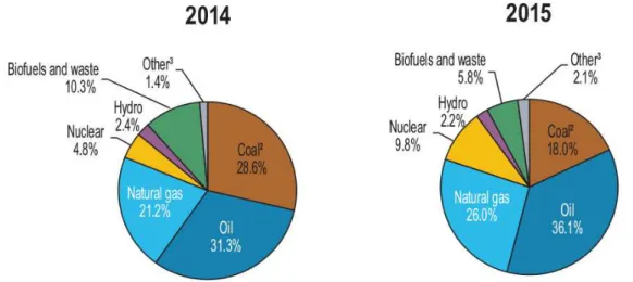
an attractive source as it is abundant and free of CO2 [1, 2]. Figure 2.1 shows the energy
consumption of different sources in global scale reported by International Energy Agency
in 2016 [3].
Figure 2.1: Energy consumption from different sources in global scale. Other – includes geothermal, solar, wind, heat, etc.
Nanotechnology has implemented substantial advances in an attempt to attenuate the
energy crisis. In this sense, some parameters have been taken into account in the attempt
to introduce new technologies based on the conversion of solar energy. Such parameters
include: development of new materials, low cost of the materials employed, use of less
aggressive materials to the environment, high reproducibility, easy manufacturing and
direct use of sunlight without diffusion losses.
Current photovoltaic technologies can be classified by generations, based on the
ma-terials and production techniques used for their fabrication. First generation solar cells
are mainly based on crystalline silicon [4]. These types of solar cells are made of a single
junction for extracting energy from photons and their efficiency is close to the
maxi-mum theoretical efficiency of ∼33 % [5, 6]. The highest research power energy efficiency
reported for these photovoltaic (PV) cells is 20 %. However the industrial-grade cell
effi-ciency is limited to 15-18 % [7]. A drawback of this kind of PV cells is that purification
of silicon is a cost demanding task that requires high temperature processing.
Second generation solar cells are based on amorphous silicon [8], copper indium gallium
diselenide (CIGS) [9], cadmium telturide (CdTe) [10], etc. These are less efficient but less
expensive cells, and were of great interest in the 1990’s and early this century. Thin film
solar cells are designed in such a way that less material is required which results in low
cost manufacturing process.
Third generation solar cells uses organic materials such as small molecules or polymers.
These cells include polymer solar cells [11–13], dye-sensitized solar cells [14–16] and small
molecule solar cells [17], among others. They are also called excitonic solar cells (XSC)
due to its charge generation mechanism based on to the formation of excitons. A new
class of thin film solar cells currently under investigation are perovskite solar cells [18]
and show huge potential with record efficiencies beyond 20% [19] on very small areas.
Polymer solar cells or plastic solar cells, on the other hand, offer several advantages such
as a simple, quick and inexpensive large-scale production and use of materials that are
readily available and potentially inexpensive. Polymer solar cells can be fabricated with
2.2 Excitons
Excitons are quasi-particles that form when Coulomb-interacting electrons and holes
in semiconductors are bound into pair states. The term exciton can encompass a wide
variety of states with very different structures and behaviors. Electron and hole, which
are coulombically bound in an exciton, can be separated when their binding energy is
overcome. Being electron-hole pairs, excitons carry no charge, which means that they do
not contribute to electrical conduction. They do carry excitation energy, however, and
their mobility therefore is responsible for energy transport processes [22, 23].
Excitons are usually distinguished in two classes: Frenkel excitons [24] and
Wannier-Mott excitons [25]. The Wannier-Wannier-Mott exciton is a loosely bound e-h pair; the strongly
bound Frenkel exciton is practically localized within one monomer, and the constituent
electron and hole lose their identity [26]. Figure 2.2 shows a schematic overview of the
exciton formation by the absorption of the light in inorganic and organic semiconductors.
Physically, the distinction originates from the competition between two energy scales:
the electron-hole coupling and the rates for electron and hole hopping between different
molecules or atoms. The hopping rates allow the electrons and holes to move individually
between different molecules in the solid or aggregate. This charge hopping arises from the
overlap between the electron and hole orbitals on neighboring molecules. If the Coulomb
coupling between electrons and holes can be neglected, this leads to freely moving electrons
and holes, that may conduct electricity. The Coulomb interaction between electron and
hole competes with their possibility to move independently through the system and if
the interaction is strong enough it gives rise to bound electron-hole states, which appear
as discrete levels below the continuum of ionized states in which electron and hole are
essentially free. In fact, if the Coulomb attraction by far exceeds the hopping rates, the
binding between electron and hole becomes too strong for them to separate and they
always occupy the same molecule or atom [26, 28, 29].
Many technological applications envisioned for organic electronic materials, such as
organic photovoltaics (OPV) and organic light-emitting diodes (OLED), involve the
Figure 2.2: Schematic overview of the exciton formation by the absorption of the light in inorganic and organic semiconductors.
Source: Adapted from POPE AND SWENBERG (1999) [27].
by the structure and dynamics of their low-lying electronic states [23].
Figure 2.3 shows an schematic overview of the exciton formation in a molecule. An
isolated molecule in its ground state has two spin-paired electrons residing in its highest
occupied molecular orbital (HOMO). The promotion of an electron into the lowest
un-occupied molecular orbital (LUMO) leaves a hole in the HOMO, resulting in an excited
singlet or triplet state, depending on the electron’s spin state [23].
The excited state in excitonic solar cells is a highly localized and slightly bound Frenkel
exciton. Their energetics and transport are central to solar energy processes. The
sep-aration of the exciton into a free electron and free hole is the source of usable electrical
energy in third generation solar cells. The diffusion of excitons to an engineered interface
that can subsequently split them into electrons and holes remains a central challenge in
Figure 2.3: Schematic overview of the exciton formation in a molecule.
Source: RLE Center for Excitonics, Massachusetts Institute of Technology [30].
2.2.1 Singlet and triplet excitons
The ground state of the majority of organic molecules is electrically neutral and has net
spin zero. A molecule can be excited when one electron from the HOMO is promoted to the
LUMO, for instance by absorption of a photon. However, with respect to excitons that
are created through charge injection, light absorption in organic semiconductors yields
only singlet excitons and thus triplet excitons can only be formed through intersystem
crossing [31, 32].
Photons do not show strong coupling to electronic spins because electromagnetic
ra-diation does not carry any torque. The electron spin is an angular momentum that must
be conserved. Thus the assistance of spin-orbit coupling is required to enable singlet to
triplet transitions [31–33]. Triplet excitons are expected to have longer diffusion length
than singlets due to their much longer lifetime. The triplet excitons slowly decay to the
ground state since they lie in an energy state that is too low for dissociation [34]. Thus,
in-tersystem crossing does not generally contribute to charge generation and may be viewed
Figure 2.4 presents possible transitions between electronic states of an isolated molecule.
In the figure, (1) represents the absorption of a photon that brings a molecule from the
ground state S0 to the first singlet excited state S1; (transitions to higher singlet excited
states are also possible). The transition (2) results in the emission of light and is called
fluorescence. Triplet excited state T1 can be created via the intersystem crossing (4). The
radiative transition (6) is called phosphorescence.
Figure 2.4: Singlet and triplet states in a state diagram. The energies of singlet (S0 and S1 ) and triplet (T1 and Tn) states are scaled vertically. Absorption (1), fluorescence (2), intersystem
crossing (4), phosphorescence (5), nonradiative transitions (3 and 6) and photoinduced absorption (7) are presented as arrows.
Source: Adapted from MIKHNENKO et al. (2015) [31] and K ¨OHLER AND B ¨ASSLER (2009) [32].
Fluorescence and/or phosphorescence can be also referred as photoluminescence (PL)
transi-tions (3) and (6) compete with fluorescence and phosphorescence. In organic materials,
the energy stored in triplet states is not available for light emission because most of the
triplet states decay non-radiatively. And finally, the transition (7) is the absorption of a
photon that brings state T1 to higher triplet excited states Tn.
Phosphorescence, (radiative decay) of the triplet excited state to the singlet ground
state, is notoriously difficult to detect unless the emitter contains heavy atoms that
en-hance spin–orbit coupling. The latter ensures first that any primarily generated singlet
states convert to triplets, and, more importantly, that the spin-forbidden T1→S0
transi-tion becomes partially allowed and so acquires intensity [32].
2.2.2 Exciton diffusion
Organic solar cells are based on a bulk heterojunction (BHJ) architecture that can be
achieved by mixing two solutions of organic semiconductors with different
electronegativi-ties and subsequently spinning a film [11]. Their operation requires the photoexcited state
in one material to diffuse until it reaches the interface to the other material, where
dis-sociation takes place provided the energy gained exceeds the exciton binding energy [36].
For this to happen it is necessary that the size of the phase separation between the two
materials be on the same length scale than the exciton diffusion length.
The ability of photoexcited exciton states to diffuse spatially provides the basis for
many of their useful properties, especially in photovoltaics [23]. The exciton diffusion
length can be estimated by the relation [23, 31, 35]:
LD=
√
6D τ , (2.1)
whereD is the exciton diffusion coefficient and τ is the exciton lifetime.
In many organic semiconductors the singlet exciton diffusion length is of the order of
3-6 nm [36–38], while the triplet diffusion length has been reported in a wide range from
10 to 100 nm [39, 40]. Therefore, it has been conjectured that a possibly larger diffusion
2.3 Characterization
2.3.1 J×V curve
A solar cell is usually characterized by photovoltaic parameters obtained from a J×V
characteristic curve like the one shown in Fig. 2.5.
Figure 2.5: J×V characteristic curve of a solar cell.
0.0 0.2 0.4 0.6 0.8
Voltage (V) -12
-8 -4 0 4 8
Current density (mA/cm
2 )
Jsc
Voc
Jm
Vm
Pmax
Source: Own author.
In general, the photovoltaic parameters are defined as:
• Open circuit voltage (Voc): is the maximum voltage that a solar cell is capable of
supplying; that is the voltage without any load applied.
• Short-circuit current density (Jsc): is the maximum current density flowing through
a solar cell under conditions of a zero resistance load; a free flow or zero volt potential
• Fill factor (FF): is essentially a measure of quality of the solar cell. It is calculated
by comparing the maximum power to the theoretical power that would be output
at both the open circuit voltage and short-circuit current density together. The FF
can assume values between 0 and 1 and is obtained by the relation:
FF = JmVm
JscVoc (2.2)
wherePm =JmVm is obtained as the product of the photocurrent and photovoltage
at the voltage where the power output of the cell is maximum.
• Power conversion efficiency (η): is given as they ratio of the maximum power
deliv-ered by the device (Pm) to the incident power (Pin) of the light source:
η = Pm
Pin =
JscVoc×F F
Pin . (2.3)
Pinis taken as the product of the irradiance of the incident light, measured in W/m2,
with the surface area of the solar cell.
2.3.2 Equivalent Circuit Model
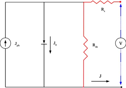
Figure 2.6 depicts the widely used equivalent circuit solar cell model. The behavior
of the J × V curve of the solar cell can be decomposed into four constituent parts:
photocurrent source, diode, series resistor, and shunt resistor.
The photocurrent source is simply the result of converting absorbed photons to free
charges by the solar cell; the diode represents electron-hole recombination at the p-n
junction; the series resistor accounts for the internal resistance of the cell to current flow;
and the shunt resistor models leakage current through the cells. Mathematically this
model is represented by the relationship [41–43]:
J =J0
exp
e(V −JRs)
nkBT
−1
+V −JRs
Rsh −Jph (2.4)
is the elementary charge, Rs is the series resistance, n is the diode ideality factor, kB is
the Boltzmann constant,T is the temperature, andRsh is the shunt resistance.
Figure 2.6: Traditional model of an equivalent circuit for a solar cell.
Jph J0 V
Rs
Rsh
J
Source: Adapted from HAINS et al. (2010) [42].
In cells with low leakage currents,Rsh ≫Rs, and the equation simplifies to:
J =J0
exp
e(V −JRs)
nkBT
−1
−Jph. (2.5)
When RS is negligible, eq. 2.5 can be rearranged at open circuit to yield [43, 44]:
Voc= nkBT
e ln
Jsc J0
+ 1
. (2.6)
Ideally Jsc increases linearly with light intensity I, Voc increases with ln(I), and the FF
is independent of I. Thus, maximum power ideally increases as ln(I). Power losses are
minimized as the values of series and shunt resistances approach the ideal values ofRs= 0
The series resistance arises from the resistance of the cell material to current flow,
particularly through the surface to the contacts, and from resistive contacts. Series
resis-tance is a major problem at high current densities, for insresis-tance under concentrated light.
The parallel or shunt resistance arises form leakage of current through the cell, around
the edges of the device and between contacts of different polarity.
A high value of Rs does not affect Voc but reduces Jsc and FF. High Rs may result
from low charge carrier mobilities and barriers to charge extraction at the electrodes. For
large area devices, resistance losses within the electrodes may also contribute significantly.
A low value of Rsh does not affect Jsc but reducesVoc and FF [45, 46].
2.3.3 External quantum efficiency
Another fundamental measurement of the performance of a solar cell is the
exter-nal quantum efficiency (EQE) also known as the incident photon-to-current conversion
efficiency (IPCE). The EQE is defined as the ratio between the number of collected
pho-togenerated charges at the electrodes to the number of incident photons at a particular
wavelength, as a function of incident energy. It is the probability that the absorption of
one photon will result in the generation of one electron that is able to flow through an
external circuit, and is typically integrated over the solar spectrum.
The EQE value corresponds to the photocurrent density produced in the external
circuit under monochromatic illumination of the cell divided by the photon flux that
strikes the cell. From such an experiment the EQE as a function of wavelength can be
calculated as [47]:
EQE(λ) = Jsc(λ)
eΦ(λ) = 1240
Jsc(λ) (A/cm2)
λ (nm)Pin (W/cm2) (2.7)
where Φ is the photon flux,Pin is the incident power, λ is the wavelength of the incident
light andeis the elementary charge. EQE values provide practical information about the
2.4 Dye-sensitized solar cells
The dye-sensitized solar cell (DSSC) technology exhibit peculiar characteristics which
differentiate them from other photovoltaic technologies. In DSSC technology the spectral
properties optimization can be done by modifying the dye, while carrier transport
prop-erties can be improved by optimizing the semiconductor and the electrolyte composition.
In 1991, O’Regan and Gr¨atzel demonstrated that a film of titania (TiO2) nanoparticles
deposited on a DSSC would act as a mesoporous n-type photoanode and thereby increase
the available surface area for dye attachment by a factor of more than a thousand [48].
A schematic representation of a DSSC is shown in Fig. 2.7. An actual DSSC contains,
in general, five components:
1. A mechanical support coated with transparent conductive oxides (TCO) such as
fluorine-doped tin oxide (FTO);
2. A semiconductor film (photoanode), usually based on TiO2 [49], SnO2 [14, 15] or
ZnO [50];
3. A dye-sensitizer adsorbed onto the surface of the semiconductor. Sensitizing dyes
have traditionally been made from ruthenium-based complexes such as cis-Bis(isothio
cyanato) bis(2,2’-bipyridyl-4,4’-dicarboxylato ruthenium(II) (N3) and Di-tetrabutyla
mmonium cis-bis(isothiocyanato)bis(2,2’-bipyridyl-4,4’-dicarboxylato) ruthenium(II)
(N719) [14, 15, 50];
4. An electrolyte containing a redox mediator such as iodide/triiodide systems [14, 15,
50];
5. A counter electrode, like platinum, capable of regenerating the redox mediator.
DSSCs are unique compared with almost all other kinds of third generation solar
cells in that electron transport, light absorption and hole transport are each handled by
different materials in the cell [51]. The sensitizing dye in a DSCC is anchored to a
wide-band gap semiconductor such as TiO2, SnO2 or ZnO. When the dye absorbs light, the
Figure 2.7: Schematic overview of a DSSC.
Source: Adapted from HAGFELDT et al. (2010) [47].
which carries the electron to one of the electrodes. A redox couple, usually comprised
of iodide/triiodide (I−/I−
3), then reduces the oxidized dye back to its neutral state and
transports the positive charge to the platinized counter-electrode.
2.4.1 Generation and recombination mechanisms
An energy level diagram showing the operation of a typical DSCC is shown in Fig. 2.8.
The first step (1) is the absorption of a photon by the sensitizer dye (D) leading to an
excited state (D∗) from which an electron is injected into the conduction band of the
semiconductor (2), leaving the dye-sensitizer in the oxidized state that is regenerated by
the redox couple (3). Unlike traditional inorganic solar cells, DSSCs require relatively large
over-potentials to drive electron injection to semiconductor and regenerate the oxidized
dye, as shown in Fig. 2.8. Typically, a potential difference between the lowest unoccupied
molecular orbital (LUMO) level of the dye and the conduction band of semiconductor is
Figure 2.8: Operating principles and energy level diagram of a typical DSSC. E n e rgy l e v e ls V oc Dye regeneration Electron injection Electron injection -5.0 eV -5.5 eV -4.0 eV -4.5 eV HOMO (D)
LUMO (D*)
Sensitizing dye Electrolyte Dye regeneration
EF
I3-/I
-I2*-/I
-Photoanode + -+ + -4 5 6 1 2 3
Source: Adapted from HARDIN et al. (2012) [51].
In some cases, recombination between charge carriers generated by photon absorption
may occur. A few possible recombination mechanisms are: direct recombination of the
excited dye reflected by the excited state lifetime (4), recombination of injected electrons
in the semiconductor with either oxidized dyes (5) or (6) acceptors in the electrolyte.
The iodide/triiodide system has been particularly successful in DSSCs because of the
slow recombination kinetics between electrons in the titania with the oxidized dye and
the triiodide in the electrolyte, which leads to long-lived electron lifetimes [52]. Iodide
reduces the oxidized dye to form an intermediate ionic species (such as I∗–
2 ) that then
disproportionates to form triiodide and diffuses to the counter-electrode, providing two
electrons per molecule, as shown in Fig. 2.8. The small size of the I−/I−
3 redox components
allows for relatively fast diffusion within the mesopores, and the two-electron system allows
The injected electron flows through the semiconductor network to arrive at the back
contact and then through the external load to the counter electrode to reduce the redox
mediator. This completes the circuit.
2.5 Organic Solar Cells
Organic semiconductors can be broadly classified into two categories: small molecules
or oligomers [53] and polymers [54]. In 1977, Shirakawaet al[55] reported on their
discov-ery of electrically conductive polymers (for which, in 2000, the Nobel Prize in Chemistry
was awarded jointly to Heeger, MacDiarmid and Shirakawa). This report boosted the
research in organic semiconductors aiming its application in new technologies. Organic
semiconductors have several unique physical properties, which offer many advantages
compared with inorganic semiconductors, such as:
• the extremely high absorption coefficients of some polymers and organic dyes in the
visible range offer the possibility to prepare very thin photovoltaic cells [56];
• many fluorescent dyes emit strongly red-shifted light compared to their absorption.
Thus, there are almost no reabsorption losses in organic light-emitting diodes [57];
• since organic semiconductors consist of molecular structures with saturated electron
systems, the number of intrinsic defects in disordered systems is much lower than
that in inorganic amorphous semiconductors having a large number of dangling
bonds [58];
• a nearly unlimited number of chemical compounds is available, and it is possible to
prepare tailor-made materials [54];
• organic semiconductors can usually be deposited on room temperature substrates
and are very well compatible with flexible substrates [20].
Figure 2.9 presents an illustration of a bulk heterejunction organic solar cell. The
typical structure, from top to bottom, consists of a transparent electrode, which is
indium oxide (ITO) or fluorine tin oxide (FTO). This is followed by an interfacial layer
composed of a hole transport material (HTM), typically an organic or metal oxide layer,
such as PEDOT:PSS[59], V2O5 [60] or MoO3 [61]. Next, the active layer, composed of
two materials: (i) the absorber, which is responsible for the photovoltaic activity of the
cell, consists of an interpenetrating network of electron donor (hole-transporting) and
(ii) acceptor (electron-transporting) materials. In state-of-the-art systems, the donor is
generally the light-absorbing material. The bottom contact typically consists of a second
interfacial layer composed of an electron transport material (ETM) as ZnO [11], SnO2 [62]
or TiO2 [63]. Finally, a low work function metal electrode, such as Ag or Al.
Figure 2.9: Schematic of a BHJ OSC: normal and inverted arquiteture.
Hole transport layer Electron transport layer
Cathode
Active layer
TCO
Electron transport layer Hole transport layer
Cathode
Active layer
TCO
Normal Inverted
Incident light Incident light
2.5.1 Mechanism of photon-to-electron conversion process
Figure 2.10 illustrates the four fundamental steps involved in the photon-to-electron
conversion mechanism for OPVs.
Figure 2.10: Fundamental mechanism of the photon-to-electron conversion process in BHJ OSCs.
Source: Adapted from SU et al. (2012) [64].
First, upon the absorption of light, an electron in the donor undergoes photoinduced
excitation from the HOMO to the LUMO of the organic material, forming a Frenkel
ex-citon [24] (coulombically bound electron (e−) and hole (h+). The ratio of the generated Frenkel excitons to the total incident photons, in terms of energy, is defined as the
absorp-tion efficiency (ηA). Excitons in organic materials have a binding energy of 0.5–1 eV [65],
the thermal energy at a room temperature of 0.025 eV. Thus, if the organic material is to
serve as an electron donor in OPVs, a second material is required as an electron acceptor
to ensure a built-in internal field at the interface to break up any excitons that diffuse
there into free carriers. The most widely used acceptor materials are fullerenes, which
have electron affinities greater than those of polymers or small molecules [64].
Second, the excitons must diffuse to the donor-acceptor (D-A) interfaces within the
diffusion length (LD ) to prevent recombination to the ground state. Because the value
of LD in organic materials is typically 10 nm [37, 38, 40], the ideal donor or acceptor
domain size should be less than 20 nm. This D-A interface concept is analogous – in
terms of charge transport – to a p-n junction in an inorganic semiconductor. The ratio
of the number of excitons that reaches the D-A interface to the total number of excitons
generated through photoexcitation is defined as the exciton diffusion efficiency (ηDE).
Third, an exciton at a D-A interface undergoes charge-transfer (CT) process at an
ultrafast pace [67] (ca. 100 fs) to form a CT exciton, where the hole and electron remain in
the donor and acceptor phases, respectively, held together through coulombic attraction.
The charge separation efficiency (ηCS) is defined as the ratio of the number of excitons
that have undergone the CT process to the number of excitons that have reached the D-A
interface.
Fourth, the CT exciton dissociates, as a result of the built-in electric field, into free
holes and electrons, which are then transported through the donor and acceptor phases,
respectively, to their respective electrodes. The transport of free carriers to the respective
electrodes occurs within a period of time ranging from nano to microseconds. The charge
collection efficiency (ηCC) is defined as the ratio of the number of carriers that have been
collected at the electrodes to the number of excitons that have undergone the CT process.
2.5.2 Relationship between the energy band and the η of a device
As mentioned in a previous section, the efficiency of a solar cell can measured as the
product of Voc, Jsc and FF. Voc is determined by recombination as well as the energy
is determined by the light harvesting and the charge separation efficiency under large
extraction fields, and FF is determined by the device series resistance, the dark current
and the charge recombination/extraction rate under low internal fields.
EQE describes the overall efficiency of the four main processes in the photovoltaic
process for OSCs, including absorption, exciton diffusion, charge separation, and charge
collection, as defined by the relation [64, 68–70]
EQE =ηA(λ)ηDE(λ)ηCS(λ)ηCC(λ) (2.8)
where λ is the wavelength of incident light. EQE values close to 100 % for a specified
wavelength indicate efficient current generation for light absorbed at that wavelength,
with limited recombination losses. Increasing recombination or reflection losses result in
lower EQE values.
The value of Jsc is influenced by the breadth of the light absorption spectrum
(de-termined mainly by the gap energy, Eg), the extent of light absorption (determined by
the thickness of the active layer), and the morphology of the active layer. Among all of
the approaches to improveη, the most common and successful strategy is developing new
low band gap donor materials to maintain a broad overlap with the solar spectrum and
ensure effective harvesting of solar photons, which leads to higherJsc [71]. Theoretically,
Jsc is defined by the relation [64],
Jsc = hc
e
Z PinEQE(λ)
λ dλ (2.9)
wherePin represents the incident power,e the elementary charge, h the Planck constant,
andcthe speed of light. Since the absorbed photon energy (Eph) is inversely proportional
to the wavelength
Eph= 1240
λ (nm) eV, (2.10)
Jsc generally increases with increasing λ across the visible and infra-red regions of the
Theoretically, the value ofVoc is linearly proportional to the difference in energy levels
between the HOMO of the donor and the LUMO of the acceptor. Therefore, to enlarge
the value of Voc , one can either lower the HOMO of the donor or raise the LUMO of
the acceptor [64, 69]. For effective charge transfer process, however, the LUMO of the
conjugated polymer must be higher [69, 72] (by at least 0.3 eV) than that of the fullerene.
Thus, Voc can be obtained by:
Voc= 1
e{ED(HOMO)−EA(LUMO)} −0.3 eV. (2.11)
Hence, the value of Voc is determined essentially by the material properties of the donor
and acceptor in the active layer, although different cathode materials also have an effect.
The value of{E(D(HOMO)−EA(LUMO)}/e is equal to the built-in potential (Vbi).
2.5.3 Doping of organic semiconductors
Due to the very different structure of organic and inorganic semiconductors, one can
expect significant differences in the properties of doped layers. However, there are many
similarities in the basic properties of the doping process. Doping inorganic semiconductors
by controllably introducing impurity atoms is the basis of several functionality in today’s
electronic devices. It allows tuning the energy level alignment at interfaces between
differently doped materials and at interfaces to metal contacts. Dopant atoms in a highly
pure material are covalently bonded to the surrounding matrix, where they introduce
electronic defect states in the fundamental gap of the semiconductor [73]. The basic
principle of doping in inorganic semiconductors is illustrated in Fig. 2.11.
Key differences in the doping behavior are caused by the fact that the transport
is driven by electron hopping in a distribution of more or less localized states. A major
impact on the transport properties in organic semiconductors can be expected in particular
when the frontier (HOMO/LUMO) molecular orbitals of the impurities have energies that
fall within the HOMO-LUMO gaps of the pure molecules. One distinguishes between deep
traps (when the trapping energy is much larger than kBT and shallow traps (when the
Figure 2.11: Doping mechanisms of molecular p-type and n-type doping. In p-type doping the molecular dopant acts as acceptor and in n-type doping as donor. A sufficient energetic overlap of matrix and dopant energy levels is required for efficient doping.
Source: Adapted from WALZER et al. (2007) [74].
In purely organic compounds, emission from a spin triplet state, i.e. phosphorescence,
is forbidden by spin-selection rules and it is thus only very weak. When a heavy metal
is incorporated in the otherwise organic structure this allows for a spin flip, so that
emission becomes possible and is strong. Knowledge of electronic processes involving the
triplet state is necessary not only because the understanding of the electronic structure of
organic semiconductor is incomplete without it, but also because the triplet state plays a
significant role in device applications. As the name suggests, there are three degenerate
Recently, it has been shown that doping the active layer of BHJ OSCs with magnetic
nanoparticles (MNPs) improves their photovoltaic parameters [11, 33, 59, 76]. Currently
there are two non-exclusive possible explanations. One claim is that a coercive electric
field generated by dipole interactions from magnetic MNPs dispersed in the active layer
increases the driving force that dissociates excitons on the donor/acceptor interfaces [59,
76]. The other claim is that a spin-orbit coupling [11, 33] due to the presence of NP
magnetic moments increases the efficiency of intersystem crossing process in the device,
and thus extends the lifetime (and diffusion length) of the photogenerated excitons.
2.5.4 Donor and acceptor materials
OSCs in which the photoactive layer is composed of a semiconductor polymer (electron
donor) and a fullerene derivative (electron acceptor) have been subject of intense research.
Experimental data from BHJ solar cells are based on the combination of a variety of donor
and acceptor materials fabricated in different laboratories and characterized by different
techniques. Most OSCs are made with bulk heterojunctions wherein an electron donating
polymer and an electron accepting fullerene derivative form nanoscaled interpenetrating
networks allowing efficient exciton dissociation and carrier transport [72, 77].
The polymer donor serves as the main solar light absorber and as the hole transporting
phase, whereas the small molecule transports electrons. Therefore a wide optical
absorp-tion range (to match the solar spectrum), large extincabsorp-tion coefficients, and large carrier
mobilities are basic requirements toward the design of ideal photoactive blends [54].
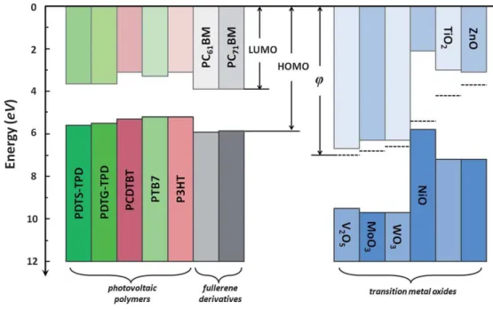
Figure 2.12 shows the HOMO and LUMO energy levels of some of the state-of-the-art
photovoltaic polymers, electron accepting fullerene derivatives and the electron affinities
and ionization energies of high/low work function metal oxides.
A fundamental difference of organic photovoltaic (OPV) compared with inorganic
photovoltaic materials is the creation of strongly bound electron–hole pairs (excitons)
upon absorption of light in the organic semiconducting materials. The energy which is
required to split an exciton is in the range of 100–400 meV compared to a few meV
electric field is not sufficient to dissociate these excitons. In order to split excitons into
free charge carriers, the energy can be provided in the presence of an electron accepting
material with a different electron affinity than the donor material [78].
Figure 2.12: The energy level diagram of state-of-art photovoltaic polymers, electron-accepting fullerene derivatives, and transition metal oxides.
Source: CHEN et al. (2012) [77].
2.5.5 Electron and hole transport materials
Figure 2.12 shows some p-type and n-type materials used as interfacial layer in OSCs.
Metal oxides can be p-type and n-type materials, depending on the position of the valence
band and conduction band. For a p-type contact material, the valence band of the metal
oxide is required to match the HOMO of the polymer. For an n-type material, electron
transfer from the LUMO of the acceptor to the conduction band of the metal oxide is
required [78].
Poly(3,4-ethyl-enedioxythiophene) (PEDOT) is widely used as a solution processed
PEDOT is doped with Poly(styrene sulfonate) (PSS) for improved conductivity and
sol-ubility in protic solvents. Additionally, p-type transition metal oxides (TMOs) have been
successfully introduced in OPV. High work-function TMOs like V2O5 [11] or MoO3 [61]
as interlayers on the anode side have been evidenced to allow for efficient hole extraction.
TiO2 [63], ZnO2 [11] and SnO2 [62] are extensively studied n-type materials for
inter-facial layers in OPV devices. These materials are transparent in the visible light spectrum
but absorb ultraviolet (UV) light. The thickness of the interfacial layer is tunable without
absorption losses in the visible (VIS) light and thus can additionally act as optical spacer.
n- and p-type semiconductivity in metal oxides are, in general, due to the intrinsic
point defects such as atomic vacancies present in the oxides. These metal oxides form
Ohmic contacts with photovoltaic polymers and fullerenes through favorable vacuum level
shift, energy level bending and Fermi level pinning at the polymer-electrode interfaces. In
addition, the use of oxide interlayers circumvents the direct contact between a photoactive
polymer and electrodes, where high densities of carrier traps or unfavorable interface
dipoles hinder efficient charge collection [77].
2.6 Oxide nanoparticles
2.6.1 Tin oxide
Tin dioxide (SnO2) is a typical wide band gap n-type semiconductor with direct band
gap of about 3.6 eV at room temperature. It is one of the most widely used semiconductor
oxide due to its chemical and mechanical stability [79] and excellent optical and electrical
properties [80, 81]. It has a rutile-type tetragonal crystal structure with a P42/mnmspace
group [82, 83]. Its unit cell consists of two Sn4+ and four O2− ions with each tin cation coordinated by six oxygen anions in the corners of a regular octahedron. Each oxygen
anion is surrounded by three Sn4+ ions which approximate the corners of an equilateral
triangle [83] as shows the Fig. 2.13. Tin oxide has many technological applications such as
in solar cells [11, 14, 62], photocatalytical activity [84], gas sensors of toxic materials [85,
Figure 2.13: Schematic representation of tin oxide structure.
Source: Own author.
2.6.2 Oxide diluted magnetic semiconductors
Oxide diluted magnetic semiconductors (O-DMS), where transition metal (TM) atoms
of 3d valence electrons are introduced into the cationic sites of the semiconducting host
lattice, have attracted the interest of researchers due to their potential use in future
spintronic and magneto-optical devices [88–90]. The discovery of room temperature
fer-romagnetism (RTFM) in Co-doped TiO2 [91], ZnO [92] and SnO2 [93] systems has played
a crucial role in expanding the field of DMS to oxides, leading to a rapid development
of new materials for application in advanced technology. As a result, intensive attention
has been focused on O-DMS such as Fe-doped ZnO [94], SnO2 [95], and TiO2 [96]. One
of the main features of these systems is that they can exhibit an intrinsic ferromagnetism
at room temperature or above. Among the different semiconductor materials, the oxides
with wide band gap such as TiO2 and SnO2 has been a subject of recent investigations
due to their potential applications in the emerging fields such as photovoltaic cells [11]
and anodes for lithium ion batteries [87].
2.6.3 Spinel ferrites
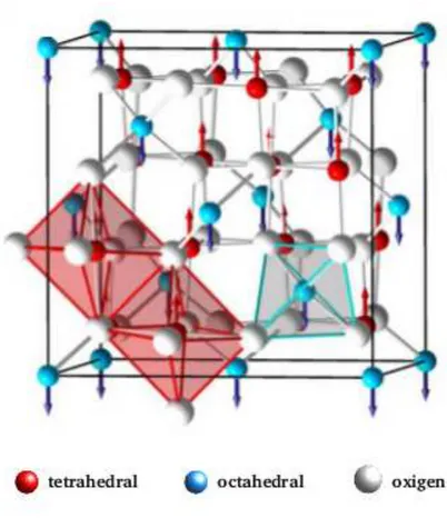
Ferrites are chemical compounds with the formula of AB2O4, where A and B represent
and hexaferrite structures [97]. Spinel ferrite structure is shown in Fig. 2.14. Cations have
either four-fold or six-fold coordination forming tetrahedra A and octahedra B sublattices
that are arranged in a close packed arrangement with respect to each other. A cations
reside on 8 of 64 available tetrahedral sites whereas B cations reside on 16 of 32 available
octahedral sites. Oxygen anions form a close packed structure and contribute 32 ions that
electrically balance the unit cell [97]. The overall symmetry of oxygens is fcc (face centered
cubic), which defines two types of interstitial sites. The space group is Fd3m[97–99].
Figure 2.14: Schematic representation of spinel ferrite structure.
Source: SUTKA AND MEZINSKIS (2012) [100].
Spinel ferrite nanopaticles (SFNPs) are in the spotlight of current nanoscience due