HEAT TRANSFER AND STRUCTURE STRESS ANALYSIS
OF MICRO PACKAGING COMPONENT OF HIGH POWER
LIGHT EMITTING DIODE
byChih-Neng HSU a*, Yu-Hao CHANG b, Chang-Yuan LIU c,
Shih-Hao FANG a, and Chun-Chieh HUANG a a
Department of Refrigeration, Air Conditioning and Energy Engineering, National Chin-Yi University of Technology, Taichung City, Taiwan, R.O.C.
b
Institute of Precision Mechatronic Engineering, Minghsin University of Science and Technology, Hsinchu County, Taiwan, R.O.C.
c
Department of Mechanical Engineering, Minghsin University of Science and Technology, Hsinchu County, Taiwan, R.O.C.
Original scientific paper DOI: 10.2298/TSCI1305277H
This paper focuses on the heat transfer and structural stress analysis of the mi-cro-scale packaging structure of a high-power light emitting diode. The thermal-effect and thermal-stress of light emitting diode are determined numerically. Light emitting diode is attached to the silicon substrate through the wire bonding process by using epoxy as die bond material. The silicon substrate is etched with holes at the bottom and filled with high conductivity copper material. The chip temperature and structure stress increase with input power consumption. The mi-cro light emitting diode is mounted on the heat sink to increase the heat dissipa-tion performance, to decrease chip temperature, to enhance the material struc-ture reliability and safety, and to avoid strucstruc-ture failure as well. This paper has successfully used the finite element method to the micro-scale light emitting diode heat transfer and stress concentration at the edges through etched holes.
Key words: heat transfer, structure stress, light emitting diode, micro packaging
Introduction
Since Edison invented the first lamp, the lamp technology has developed toward pow-er-saving, low pollution, and long life design. Light emitting diode (LED) is a new generation of solid state lighting with superior characteristics, such as high efficiency, high brightness, long life, low power consumption, low pollution, full color display, adaptability to any climate, anti-dust, and so on. LED has become a highly important lighting tool [1-12]. This paper inves-tigates the heat transfer and thermal stress for high-power LED micro-scale design and analysis to reduce the chip hot spot temperature. Thermal effect significantly impacts the micro structure package design; hence, thermal cooling was employed to investigate the problem. Micro LED could reduce power consumption, thermal cooling, and thermal stress problems.
Design and structure of micro LED and heat sink model
In order to increase the LED chip lighting brightness, the new design cup-shaped micro LED reflector structure was employed for the analysis model, as shown in fig. 1. Figure
––––––––––––––
2 and tab. 1 illustrate the schematic of the micro LED packaging structure, position, and size. The chip is made of indium gallium nitride (InGaN) with size 0.4 × 0.4 × 0.005 mm. The chip die attached is 0.4 × 0.4 × 0.07 mm. The micro LED new design ma-terial parameters and properties are shown in tab. 2.
The solder dimension (0.4 × 0.4 × 0.025 mm) used Sn63/Pb37 as a buffer layer between the substrates. The substrate is a silicon wafer material with im-proved heat dissipation and is suitably integrated with silicon-based IC or MEMS micro devices, creating an etching angle of 54.7°. The etching depth (MH) is 0.3 mm. The base of the substrate thickness (MT) is 0.1 mm. The LED chip
tem-perature could achieve faster cooling if the substrate is wet downward, etched with holes, and placed in a high ther-mal conductivity material. The etching width is 1.8 × 1.8 × 0.3 mm, and the pitch (MS) is 0.1 mm. The LED chip
path of the wire connection likewise requires consideration, and thus the LED chip was etched around the four guide wire holes as the path of the wires connecting the chip, as shown in figs. 1 and 2.
The LED model needs to match the printed circuit board (PCB), and the PCB material can affect the thermal conductivi-ty of the LED packaging structure. Thus, this analysis model would adopt the alu-minum metal core PCB with a thickness of 1 mm, as shown in fig. 3. The analysis model was established conveniently and the PCB structure was simplified, as shown in the cross-sectional view in fig 4. Figure 5 shows the LED 3 × 3 array mod-el, in which the distance between the LED was 0.5 mm.
Table 2. Material parameters and properties Figure 1. Design of micro LED model and etching of the four holes
Table 1. Packaging structure position and dimension
MChip 0.005 mm MSR 0.05 mm Mθ 54.7° (angle)
MDA 0.07 mm MT 0.1 mm MS 0.1 mm
MSol 0.025 mm MH 0.3 mm MBR Radius
Figure 2. Cross-sectional view of the micro LED packaging structure design and size
Material Conductivity
coefficient [Wm–1K–1]
Coefficient of thermal expansion (CTE) [°C–1]
Young’s modulus coefficient [GPa]
Poisson’s ratio
InGaN 130.0 5.6·10–6 210 0.31
Solder 50.6 23.9·10–6 14.9 0.35
Cu 401.0 16.5·10–6 128 0.26
Sapphire 41.9 6.7·10–6 400 0.24
SiC 500.0 4.2·10–6 448 0.19
Silicone 1.8 300·10–6 6.1·10–4 0.34
Si 148.0 1.56·10–6 190 0.30
When the model was completed, the boundary conditions and materials must be set including material property, heat transfer model, power consumption, light emission, thermal stress analysis, and so on.
Figure 3. Micro LED mounted on PCB for single LED
Figure 4. Cross-sectional view of the micro LED packaging layers
To enhance heat dissipation more effectively and increase the structure strength, the heat sink mount on the PCB board must be configured. In this paper, the micro-scale packaging structure design was analyzed; thus, the micro LED space with heat sink and sink fin also con-sidered the ratio of height and space. During this study, all of
the heat sinks would adopt uniform rectangular shapes be-cause of its convenient design for analysis and manufacture. Figure 6 shows the single micro LED, while fig. 7 shows the 3 × 3 array micro LED mounted on PCB, as well as the heat sink design and analysis model. The heat sink dimension is 15 × 15 × 1 mm, fin length is 10 mm, fin thickness is 0.5 mm, and the distance between fins is 2 mm. This design enhanced the fin contact area, which could increase heat transfer, re-duce hot spot temperature, and reach uniform temperature
thermal cooling. These heat transfer analysis results can be transferred to the structure model as the initial conditions for the thermal stress study. The set-up parameters are as follows: hc =
2-10 W/m2K for under 1 W, hc = 10 W/m2K for 2 W, and hc = 25 W/m2K for 3 W.
Figure 6. Cross-sectional view of the single LED of the micro LED mounted on the PCB and heat sink
Figure 7. Cross-sectional view of the 3 × 3 arrays of the micro LED mounted on the PCB and heat sink
The LED structure model has a micro-scale packaging structure, and the wire bond-ing heat transfer and thermal stress distribution of such design would be investigated. LED thermal-effect and thermal-stress were likewise simulated by using the ANSYS software for the finite element method, in which heat transfer is combined with conduction, convection, and thermal radiation. Thermal stress is equivalent to the Von Mises criterion. The LED was attached to the silicon substrate through the wire bonding process by using epoxy as the die
GaN
Sapphire
Solder (Sn63/Pb37)
Al
Cu
Si
Thermal pad [7 Wm–1K–1]
Silicone
bond material. The geometries of the finite element model were close to those of a typical LED device. In order to address the heat convection, the LED model would be added to the heat convection coefficient (hc) experience to formulate the solution thermal effect as [11]:
3 2 3
[3 139 10 exp( 1 311 10 ) ∆ Pr]n
a
c avg . ch
ch
k
h C . . T L T
L
−
= ⋅ ⋅ − ⋅ ⋅ ⋅ ⋅ (1)
where ∆T is Tsurface – Tambient, Tavg. is (Tsurface – Tambient)/2, ka is the air conductivity coefficient, Lch is the characteristic length of geometries, n = 0.25; C = 0.27–0.59; Pr is the Prandtl
num-ber = ν/α, ν is the momentum diffusivity, α is the thermal diffusivity, and Pr = 0.72 for air.
Results and discussion
To enhance the micro LED thermal cooling and reduce the thermal stress concentra-tion effect, the single micro LED mounted on the PCB and heat sink was investigated by us-ing hc = 2 W/m2K, hc = 10 W/m2K, and hc = 25 W/m2K at 1 W, 2 W, and 3 W, respectively.
The 1 W analysis results showed that the heat transfer Tj temperature steady-state is 44.6 °C,
as shown in fig. 8. At the same time, the Tj temperature is 64.2 °C and 83.8 °C when micro
LED was added to the 2 W and 3 W power consumption analyses, as shown in figs. 9 and 10, respectively. Thus, the thermal effect of the micro LED packaging structure mounted on the PCB and heat sink can be improved.
Figure 8. Single micro LED heat transfer results for 1 W – hc = 2 W/m2K*
Figure 9. Single micro LED heat transfer results for 2 W – hc = 10 W/m2K*
Figure 10. Single micro LED heat transfer results for 3 W – hc = 25 W/m2K*
From the heat transfer analysis results, the 1 W thermal stress effect showed that the thermal stress concentration location maximum steady-state is 142.9 MPa, as shown in fig. 11. At the same time, the maximum steady-state is 152 MPa and 160 MPa when micro LED was added to the 2 W and 3 W power consumption analyses, as shown in figs. 12 and 13.
Figure 11. Single micro LED thermal stress concentration results for 1 W – hc = 2 W/m2K*
Figure 12. Single micro LED thermal stress concentration results for 2 W – hc = 10 W/m2K*
Figure 13. Single micro LED thermal stress concentration results for 3 W – hc = 25 W/m2K*
The micro LED 3 × 3 arrays mounted on the PCB and heat sink was also investi-gated at 1 W, 2 W, and 3 W. The 1 W Tj temperature steady-state is 48.6 °C, as shown in fig.
––––––––––––––
*
14. At the same time, the Tj temperature steady-state is 72.3 °C and 95.9 °C when the micro
LED was added to the 2 W and 3 W power consumption analyses, as shown in figs. 15 and 16, respectively. Thus, the micro LED 3 × 3 array packaging structure mounted on the PCB and heat sink could improve the Tj thermal effect. Figure 17 compares the results of the micro
LED 3 × 3 array Tj temperature heat transfer analysis with/without heat sink. Heat sink could
help decrease the micro LED Tj temperature, which ranges 30-41% and under the
specifica-tion value of 100 °C.
Figure 14. Micro LED 3 × 3 arrays heat transfer results for 1 W – hc = 2 W/m2K*
Figure 15. Micro LED 3 × 3 arrays heat transfer results for 2 W – hc = 10 W/m2K*
Figure 16. Micro LED 3 × 3 arrays heat transfer results for 3 W – hc = 25 W/m2K*
From the LED 3 × 3 array heat transfer analysis results, the 1 W thermal stress effect indicated that the stress concentration location maximum steady-state is 162.6 MPa, as shown in fig. 18. At the same time, the maximum steady-state is 191.5 MPa and 220.5 MPa when the micro LED was added to the 2 W and 3 W power consumption analyses, as shown in figs. 19 and 20, respectively. Figure 21 compares the results of the micro LED 3 × 3 arrays thermal stress concentration analysis with/without heat sink. The heat sink could be decreased with micro LED thermal stress concentra-tion of 29% to 57%.
Figure 18. Micro LED 3 × 3 arrays thermal stress results for 1 W – hc = 2 W/m2K*
Figure 19. Micro LED 3 × 3 arrays thermal stress results for 2 W – hc = 10 W/m2K*
Figure 20. Micro LED 3 × 3 arrays thermal stress results for 3 W – hc = 25 W/m2K*
Figure 22 shows the micro LED comparisons with single and 3 × 3 arrays for Tj
temperature analysis using hc = 2-25 W/m2K. Figure 23 compares the micro LED of single
and 3 × 3 arrays for thermal stress analysis using hc = 2-25 W/m2K.
Thermal stress concentration location load effect is likewise added to the internal material bonding crack when the micro LED packaging structure temperature increased.
––––––––––––––
*
For color image see journal web site
Figure 17. Micro LED 3 × 3 arrays Tj
temperature analysis results comparison with/without heat sink
160 140 120 100 80 60 40 20 0
Tj
[°C]
LED power [W] LED 3 × 3 arrays for PCB LED 3 × 3 arrays for PCB and heat sink
Thermal stress concentration effect would be decreased from 13% to 33%, and reducing the structure fracture of the Tj temperature could
en-hance heat conduction.
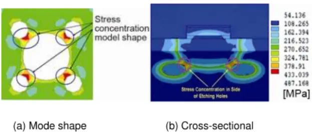
From analysis results (fig. 24), we could be clearly determined the micro LED thermal stress concentration location at the side of the etching holes, and similarly the golden wire bonding po-sition.
Figure 24. Thermal effect temperature distribution*
Figure 25(a) shows the thermal stress concen-tration location mode shape and fig. 25(b) shows the cross-sectional view thermal stress concentra-tion value.
(a) Mode shape (b) Cross-sectional
Figure 25. Micro LED thermal stress concentration location at the edge of etching through holes*
In the future, the micro LED packaging struc-ture design should carefully pay attention to the golden wire bonding and fabrication process at the edge of etchings through the heat transfer ef-fect and stress concentration of holes location.
Conclusions
This paper has successfully used the finite element method for the simulation and analysis of micro LED packaging structure heat transfer and thermal stress concentration location at the edge of etching through holes. The packaging could be improved by wire bonding and fa-brication structure thermal effect zone. This micro-scale LED design has used a reflector cup
––––––––––––––
*
For color image see journal web site
Figure 21. Micro LED 3 × 3 arrays thermal stress concentration analysis results comparison with/without heat sink
Figure 22. Micro LED comparison with single and 3 × 3 arrays for Tj results – hc = 2-25 W/m2K
Figure 23. Micro LED comparison with single and 3 × 3 arrays for thermal stress concentration results – hc = 2-25 W/m
2
K 500
400
300
200
100
0
Thermal stress [MPa]
LED power [W]
0 1 2 3 4
LED 3 × 3 arrays for PCB LED 3 × 3 arrays for PCB and heat sink
100
80
60
40
20
0 Tj
[°C]
LED power [W] LED 3 × 3 arrays for PCB and heat sink
Single LED for PCB and heat sink
0 1 2 3 4
300
250
200
150
100
Thermal stress [MPa]
LED power [W]
0 1 2 3 4
LED 3 × 3 arrays for PCB and heat sink
to improve the InGaN light emitting efficiency. According to the simulation and analysis re-sults, the important conclusions are summarized as follows.
● The micro-scale LED model temperature and thermal stress are proportional to the input power consumption. Heat convection coefficient (hc) enhancement and improvement could help LED thermal cooling, reduce Tj temperature, and increase long life. Thermal stress concentration zone was found at the edge of etching through holes.
● The increase of the heat transfer area of the micro LED mounted on the PCB and heat sink enhances the thermal cooling, increases structure strength, and decreases the thermal stress concentration effect. LED array heat transfer temperature and thermal stress concentration zone could likewise be increased. Thus, the heat convection coefficient cooling of the LED element must be improved by using stable, safe, and reliable packaging materials.
● Thermal stress concentration zone would decrease and the overall structure would be enhanced when the micro LED Tj temperature decreases. Thermal stress concentration
zone would increase and the overall structure would be weakened when the micro LED Tj temperature increases.
Acknowledgments
The authors would like to thank the Engineering Division of the National Science Council of the Republic of China, Taiwan, for financially supporting this research under con-tract number NSC 100-2815-C-167-002-E and NSC 101-2622-E-167-014-CC3.
References
[1] Arik, M., et al., Thermal Challenges in the Future Generation Solid State Lighting Applications: Light Emitting Diodes, The Eighth Intersociety Conference on Thermal and Thermomechanical Phenomena in Electronic Systems (ITHERM 2002), San Diego, Cal., USA, 2002, pp. 113-120
[2] Arik, M., et al., Thermal Management of LEDs: Package to System, Third International Conference on Solid State Lighting, Proceedings of SPIE, SPIE, Bellingham, Wash., USA, 2004, Vol. 5187, pp. 64-75 [3] Tsou, C. F., Huang, Y. S., Silicon-Based Packaging Platform for Light-Emitting Diode, IEEE
Transac-tionson Advanced Packaging, 29 (2006), 3, pp. 607-614
[4] Yuan, L., et al., Thermal Analysis of High Power LED Array Packaging with Microchannel Cooler, 7th International Conference on Electronic Packaging Technology (ICEPT’06), Shanghai, China, 2006,
pp. 1-5
[5] Lee, C. Y., Liu, J. L., Illumination Based on High-Power White Light-Emitting Diode Array, Interna-tional Journal of Green Energy, 9 (2012), 5, pp. 421-429
[6] Christensen, A., Graham, S., Thermal Effects in Packaging High Power Light Emitting Diode Arrays, Applied Thermal Engineering, 29 (2009), 2, pp. 364-371
[7] Vipradas, A., et al., A Parametric Study of a Typical High Power LED Package to Enhance overall Thermal Performance, 13th IEEE Intersociety Conference on Thermal and Thermomechanical Pheno-mena in Electronic Systems (ITherm), San Diego, Cal., USA, 2012, pp. 308-313
[8] Yan, B., et al., Influence of Die Attach Layer on Thermal Performance of High Power Light Emitting Diodes, IEEE Transactions on Components and Packaging Technologies, 33 (2009), 4, pp. 722-727 [9] Feng, W. F., et al., Packaging and AC Powering of LED Array, Proceedings, 60th Electronic
Compo-nents and Technology Conference (ECTC), Las Vegas, Nev., USA, 2010, pp. 512-514
[10] Jang, S. H., Shin, M. W., Thermal Analysis of LED Arrays for Automotive Headlamp with a Novel Cooling System, IEEE Transactions on Device and Materials Reliability, 8 (2008), 3, pp. 561-564 [11] Chi, W. H., et al., Analysis of Thermal Performance of High Power Light Emitting Diodes Package,
10th Electronics Packaging Technology Conference (EPTC), Singapore, 2008, pp. 533-538
[12] Robert, F., Karlicek, J., High Power LED Packaging, IEEE Conference on Lasers and Electro-Optics (CLEO), Baltimore, Md., USA, 2005, Vol. 1, pp. 337-339