Multiangular and Spectral Ellipsometry for Semiconductor Nanostructures Classification
A.A. Goloborodko*, M.V. Epov, L.Y. Robur, T.V. Rodionova
Taras Shevchenko National University of Kyiv, 64/13, Volodymyrska Str., 01601 Kyiv, Ukraine
(Received 11 November 2013; published online 20 June 2014)
The possibilities of multiparameter determination of semiconductor nanostructures based on spectral dependencies of polarized radiation reflection coefficient Rp, Rs on the incidence angle in the range of 200-800 nm are investigated. Experimental data have shown high sensitivity of reflection coefficients angular dependence to the type of polycrystalline structures at the same film thickness. The presence of additional extremums in spectral dependence of refraction and absorption indexes is detected; this could be connected with grain size of polycrystalline structure and type of grain boundaries. The possibility of multiparameter optical research of properties and thickness of semiconductor layers on Si substrate is shown.
Keywords: Polysilicon film, Spectral ellipsometry, Reflection coefficient, Refraction index, Absorption index.
PACS numbers: 78.40.Fy, 78.66.Jg
1. INTRODUCTION
Upon the development of nanotechnologies the meth-ods of nondestructive, multiparameter, express, local determination of properties of semiconductor structures become the most essential. For most widespread layered film structures the significant properties are layer thick-ness and basic optical properties such as refractive index (n) and absorption index (). On the one hand, this is connected with informativeness of these parameters, and on the other hand – with significant dependence of lay-ers properties on their thickness d (preparation condi-tions [1], thermal treatment [2], oxidation and exposure [3]). Dependencies n(d) and (d) for thin layers, obtained at the same wavelengthб aren’t constant and can have different shapes first of all as a result of differences in technological processes of structure preparation [1]. Therefore, use of any parameter value from tabulated or literature data can be erratic and lead to considerable inaccuracy in the diagnosis of other properties.
The way out of this situation is determination of set of related parameters within the same method and measurement system, which allows determining a set of properties during one act of measurement. However, currently the optical methods that allow simultaneous determining of refractive and absorption indexes, layer thickness for absorbing and non-absorbing materials aren’t well developedг юn recent investigations of local defects on the silicon surface [4] the wavefront meas-urements and its dependence from surface reflectance were used. In paper [5] the influence of local refraction and absorption indexes inhomogeneties on the reflection coefficient was mentioned. It should be noticed that higher precision of parameters estimation using data of wavefront measurement can be achieved by step-by-step sequential probing in two orthogonal polarizations [5, 6]. In this paper different possibilities of multiparameter determination of properties of semiconductor structures using data about spectral dependence of reflection coeffi-cients of p- and s- polarized radiation (Rp and Rs) on the angle of incidence in are investigated. Moreover, the possibility of reconstruction of spectral distribution of refraction and absorption indexes is studied.
2. POLYCRYSTALLINE SILICON FILMS
2.1 Preparation
Silicon films were prepared by low-pressure chemical vapour deposition from silan/argon mixture. Films were deposited on thermally oxidized (thickness of SiO2 is 100 nm) single crystal silicon wafers with the thickness of about 2 m. Polycrystalline Si samples were obtained by increasing deposition temperature (Td) over 900 K, for amorphous films samples Td 830 K. Some samples were doped with phosphorus by ion implantation, ther-modiffusion, under deposition (in situ) and annealed within the temperature range 1200-1500 K in nitrogen ambient. Thus the structure of poly-Si films depends on deposition conditions and temperature and forms three main structures: fibrous, dendritic or equiaxed [7].
The fibrous microstructure is formed in undoped poly-Si films (thickness d 70 nm) under deposition temperature over 900 K. The dendritic structure is formed from amorphous or amorphous-crystalline states under annealing at temperature from 1100K to 1200K. Equiaxed structure results from recrystalliza-tion of high doped (nP 1020 1021 m– 3) poly-Si films under temperature over 1300 K. More details about different film structures obtaining and their typical structure charachteristics can be found in [7].
2.2 Basic Theory
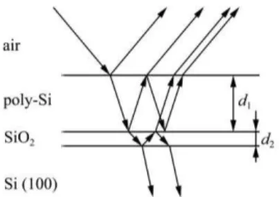
For describing the characteristics of the light reflect-ed from multilayer samples the model must have differ-ent layer thickness and boundaries with differdiffer-ent refrac-tion indices, which correspond to the following media: air, poly-Si film, SiO2, massive substrate of Si (Fig. 1).
Fig. 1– Scheme of the light reflection from the multilayer structure
wave reflects and refracts on each next edge. So, the final result will depend on the coefficients of refraction and reflection, optical path length and phase shifts be-tween p- and s- components. The reflection coefficient for three-layer system: poly Si-SiO2-Si(100) one can write as: 2 1 2 2 1 2 2 2 12 23 01 2 12 23 2 2 12 23 01 2 12 23 e e 1 e e e 1 e 1 e i i i i i i i r r r r r R r r r r r
R , (1)
where r01, r12, r23 are Fresnel reflection coefficients [8] at the interface air- poly Si, poly Si-SiO2, SiO2-Si(100) correspondingly; - phase thickness of the film:
2 22 i sin
i in
d n i
, (2)
where di is i-th layer thickness, is probe radiation wavelength, in is incidence angle of radiation. Thus, the ellipsometry equation for such system is:
2 1 2 2 1 2 2 1 2 2 1 2 2
12 23 2
01 2 12 23 2 2 12 23 01 2 12 23 2 2 12 23 01 2 12 23 2
12 23 2
01 2 12 23 e e 1 e tg e e e 1 e e 1 e 1 e e 1 e 1 e i
p p i
p i p p i i i s s s i s s i i s s s i s s i
p p i
p i p p r r r r r r r r r r r r r r r r r r r r
, (3)
where and stand for relative amplitude and phase change [8]. It's not difficult to notice, that reflection coefficient contains phase factor, which corresponds to phase incursion at wave propagation in multilayered medium. This, in turn, proves the probability of inter-ference phenomenon appearance and reveals as oscilla-tions of angular and spectral dependencies of reflection coefficient [9].
It's necessary to solve direct ellipsometry problem, when ellipsometric parameters ( and ) of reflected wave are calculated using known characteristics of re-flection systems, and inverse problem, when parame-ters of test system can be found using measured values of polarization characteristics of reflected wave, while interpretating ellipsometric measurements. It's im-portant to mention, that it's necessary to solve tran-scendental equation (3) for solving the inverse problem
of obtaining refractive and absorption indexes of film. For its solution the numerical analog of diagrams method was used [10]. Calculation of ellipsometric pa-rameters was performed for fixed angle of incidence or wavelength (eq. 3), varying layer thickness and its re-fraction index, with adding filling factors changing [11]. A set of curves converging at one value was build using the obtained results.
3. EXPERIMENTAL SET-UP
The photoelectric ellipsometer is the most suitable for spectral ellipsometry measurements, which in contradis-tinction from compensated ellipsometer doesn't require any compensator and has less measurement time. The operation principle of such ellipsometer is based on photo-electric Beattie method [10]. The essence of method is following: linearly polarized light beam falls on the surface of investigated object at arbitrary angle, and azimuth of polarizer (angle between electric vector of light wave and plane of incidence) equals 45.
Elliptical polarization of reflected light is analyzed us-ing linear polarizer, which is sequentially set at 0, 45 and 90 azimuth, measuring corresponding intensity of reflected light I0, I45, I90. Unknown ellipsometric parame-ters are computed by formulas:
0 90
tg I
I
, (4)
45 90 0
90 0
2 cos
2
I I I
I I
. (5)
The scheme of such device is shown at Fig. 2.
Fig. 2– Block-diagram of spectral photoelectric ellipsometer
A source of light in this device is halogen lamp IEC 60061-1 (7004-73) in range of 450-800 nm and ultra-high pressure arc xenon ball lamp DKsH-150 with reg-ulated power supply in range of 240-578 nm. Polarizer (Glan prism) provides linear polarization of the light wave. It is mounted in frame, fitted with device for po-larizer rotation around the direction of light beam propagation and the system of azimuth in measure-ment. The unit for analyzing the polarization ellipse of reflected light wave also comprises Glan prism with positioner mechanism.
sam-ple with mechanism that allows rotating in vertical and horizontal plane and mechanism of translational dis-placement of platform in perpendicular direction to the surface is placed on the goniometer axis.
Measurement error of refraction and absorption in-dexes (estimated from the set of photovoltage meas-urements) doesn't exceed 1.5 % in UV and visible range and 2.5 % in IR range of electromagnetic spectrum.
4. RESULTS AND DISCUSSION
Ellipsometric measurements were performed for mir-ror reflection of optical radiation with illuminating beam aperture 5 mm at different angle of incidence on the sam-ple. The silicon wafers Si (100) and amorphous silicon film Si (100) + Si (a) (film width was about 700 nm) were test-ed as the reference samples. The value of calculattest-ed spec-tral distribution of refraction (n) and absorption () index-es for bulk silicon is shown at Fig. 3. Such spectrum corre-sponds to known data from literature [12].
Fig. 3– Spectral dependence of refraction and absorption indexes for Si (100)
The amorphous silicon as well as the polycrystalline silicon is the isotropic matter, thus the films of amor-phous or polycrystalline Si on the same substrate have no significant polarization differences. As one can see from Fig. 4 the dependence of reflection coefficients for the amorphous silicon film don't differ from the depend-ence, obtained for continuous media, but the amorphous silicon film has other reflection coefficients (Rp and Rs) and the position of the main (pseudo-Brewster) angle.
Fig. 5 shows the similar dependencies for polysilicon films with fibrous, dendritic and equiaxed structures. As one can see, the nature of dependencies is substan-tially different for all three cases. It can be noticed that normal reflection coefficient R increases for investigat-ed structures in direction – dendritic, fibrous, equiaxed. At the same time the size of surface inhomogeneities change in other sequence, i.e. it's logical to assume, that obtained optical features are connected with mor-phological peculiarities of polysilicon films structure, not with the size of surface inhomogeneities. Results, obtained for films with different structural modifica-tions, are in good correspondence with presence of spe-cial grain boundaries and grain boundary junctions in the films. Speaking about grain boundary junctions, in [13] was shown the existence of different types of triple junctions and also the presence of multiple junctions of four and five grains, that vary in terms of quantity and interlayer spacing of boundaries for polysilicon films with mentioned structural modifications. Such influ-ence of grain boundary junctions on the optical proper-ties stipulates angular dependencies.
Fig. 4– Angular dependencies of reflection coefficient for sili-con Si (100) and for system of amorphous film on silisili-con sub-strate Si (100) + Si (a) for wavelength 633 nm
Fig. 5– Angular dependencies for reflection coefficient of poly-crystalline films with different structure at wavelength
633 nm
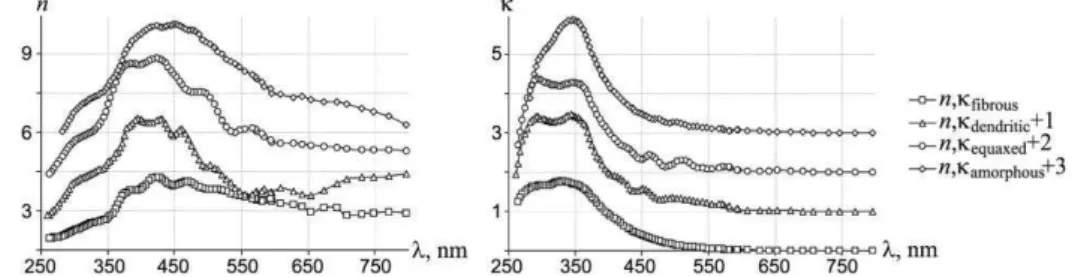
The calculated spectral dependencies of silicon films refraction and absorption indexes are shown on Fig. 6. As it can be seen from given dependencies the dendrit-ic, fibrous and equiaxed films (with the same thickness as amorphous one) show themselves on the background of amorphous film by the presence of oscillations of re-fraction and absorption indexes. This, obviously, is connected with presence of grain boundaries with dif-ferent reflection coefficients, while presence of special boundaries [14] leads to the increase of amplitude of such oscillations.
Error in spectrum reconstruction of refraction and absorption indexes dependencies from equation (3) was controlled from Kramers-Kroning relation [15]:
2
2 2 2
1 n w w
n P dw
w
, (6)where and w are frequency, P is main integral value symbol, ... is symbol of wavelength averagingг Let’s mark, that value of spectral error, specified in this man-nerб doesn’t exceed егж at Эn2() + 2() – 1)|min 4.2. Fig. 4 and Fig. 5 show the experimental angular de-pendencies of the reflection coefficient of investigated structures. Parameters of given structures, obtained from angular dependencies of reflection coefficient and from spectral dependencies of ellipsometric parameters, are listed in Table 1.
Fig. 6– Spectral dependencies of refraction and absorption indexes for silicon films with different structural modifications
Table 1– Values of characteristics of different structures, defined from angular dependencies of reflection coefficient and from spectral dependencies of ellipsometric parameters ( 633 nm)
Upper layer parameters Angular dependencies Spectral dependencies amorphous silicon n
d,
3.38 0.025
732
3.34 0.029
721
fibrous n
d,
3.44 0.015
724
3.47 0.011
711
dendritic n
d,
2.79 0.007
697
2.81 0.005
703
equiaxed n
d,
3.51 0.035
754
3.49 0.031
749
structures thickness. The application of scheme of paral-lel angular dependencies measurement with fixed sam-ple and time averaging of data can increase the accuracy of method [15].
Thereby, performed researches of different possibil-ities for multiparameter determination of structures properties, based on the analysis of angular dependen-cies of reflection coefficient and spectral dependendependen-cies of ellipsometric parameters, revealed the possibility of classification of polysilicon structures with different structural modifications.
5. CONCLUSIONS
The possibility of non-destructive determination of thickness, refraction and absorption indexes of surface
layers with different structural modifications of polysili-con is realized on the base of the measurements of reflec-tion coefficient dependencies on the incidence angle of monochromatic radiation and ellipsometric parameters dependencies on the wavelength of scanning radiation. Let's notice that carrying out of such measurements is possible for determination of film and substrates proper-ties in structures with different combinations of absorb-ing and slightly absorbabsorb-ing materials. Besides, the meas-urement errors in angular dependencies of reflected ra-diation analysis (which is simpler in hardware realiza-tion), are close to the errors of simple ellipsometric method in fixed conditions, though angular dependencies are significantly less informative.
К а а а а
а а
г г б г гЄ б г г б Тг г
в а а в . .Ш в а, в .В а, лйд1и, е1ле1 в, а а
є Rp, Rs в
зее-800 г є в
г в
' в
г
є .
К ап є б б є б в
К а а а а
г г б г г б г г б Тг г
в а а в . .Ш в , . В а ая, лйд1и, е1ле1 в, а а
И в
Rp,
Rs зее-800 г в
г
г в
в
г
К ап б б б
б г
REFERENCES
1. B. Poqany, Annalen der Physik49, 537 (1916).
2. S.W. Xuea, X.T. Zu, et al., J. Alloy. Compd. 448, 21 (2008). 3. S.A. Kovalenko, M.P. Lisitsa, Semiconductors Physics,
Quantum Electronics and Optoelectronics.4, 352 (2001). 4. A.A. Goloborodko, V.I. Grygoruk, et al., Ukr. J. Phys.53,
946 (2008).
5. N.S. Goloborodko, V.I. Grygoruk, et al., Semiconductors Phys-ics, Quantum Electronics and Optoelectronics13, 65 (2010). 6. A.A. Goloborodko, V.N. Kurashov, D.V. Podanchuk,
N.S. Sutyagina, M.M. Kotov, Proc. of SPIE7388, 73880P (2009).
7. N.G. Nakhodkin, T.V. Rodionova, phys. status solidi a123, 431 (1991).
8. H. Fujiwara, Spectroscopic Ellipsometry. Principles and Applications (John Wiley & Sons Ltd: The Atrium, Southern
Gate, Chichester, West Sussex PO19 8SQ, England: 2007). 9. O.I. Barchuk, K.S. Bilenko, et al., Nanosystems,
Nano-materials, Nanotechnologies.7, 421 (2009). 10.R.J. Archer, J. Opt. Soc. Am.52, 970 (1962).
11.A.A. Goloborodko, N.S. Goloborodko, et al., Semiconductors Physics, Quantum Electronics and Optoelectronics16, 128 (2013).
12.J.R. Beattie, G.K.T. Conn, Philos. Magazine43, 222 (1955). 13.N.G. Nakhodkin, N.P. Kulish, et al., Nanosystems,
Nano-materials, Nanotechnologies2, 793 (2004).
14.N.G. Nakhodkin, N.P. Kulish, et al., Bulletin of University of Kyiv. Series: Physics and Mathematics. 201, (2010). 15.Yu.E. Zabiyakin, Optika i Spektroskopiya.24, 828 (1968). 16.D.I. Bilenko, A.A. Sagaidachnyi, V.V. Galushka, and