Pedro Miguel Ribeiro Pereira
Mestre
Optimization Based Design of
LC
Voltage Controlled Oscillators
Dissertação para obtenção do Grau de Doutor em Engenharia Electrotécnica e de Computadores
Orientador:
Prof. Doutora Maria Helena Fino, Professora
Auxiliar, Faculdade de Ciências e Tecnologia da
Universidade Nova de Lisboa
Co-orientador:
Prof. Doutor Mário Ventim Neves, Professor
Auxiliar, Faculdade de Ciências e Tecnologia da
Universidade Nova de Lisboa
Júri:
Presidente: Prof. Doutor Paulo da Costa Luís da Fonseca Pinto
Arguentes: Prof. Doutor Francisco Vidal Fernández Fernández Prof. Doutor João Manuel Torres Caldinhas Simões Vaz
Vogais: Prof. Doutor Mourad Fahkfahk
Optimization Based Design of LC Voltage Controlled Oscillators
Copyright © Pedro Miguel Ribeiro Pereira, Faculdade de Ciências e Tecnologia, Univer-sidade Nova de Lisboa.
A Faculdade de Ciências e Tecnologia e a Universidade Nova de Lisboa têm o direito, perpétuo e sem limites geográficos, de arquivar e publicar esta dissertação através de exem-plares impressos reproduzidos em papel ou de forma digital, ou por qualquer outro meio conhecido ou que venha a ser inventado, e de a divulgar através de repositórios científicos e de admitir a sua cópia e distribuição com objectivos educacionais ou de investigação, não comerciais, desde que seja dado crédito ao autor e editor.
Acknowledgments
I would like to take this opportunity to remember, in an informal way, those who in many different ways have supported me during the long years that I took to complete this work.
Sincerely, I am deeply grateful to my supervisor, Professor Helena Fino, for her support, guidance, professionalism, patience and knowledge, both scientific and intellectual. Without her
enthusiasm and insights, priceless comments and discussions, probably most of this work would not have been possible. I will be forever grateful.
I would like to thanks to my co-supervisor, Professor Ventim-Neves, for his useful ad-vices when I faced less optimistic moments. I will never forget some of his history lessons during countless enjoyable lunches.
I also would like to express my sincere thanks to Professor Fernando Coito, for his valuable comments throughout some periods of my research. The joint work that has resulted
from our close collaboration, was fruitful.
A special word of appreciation goes to Professor Leão Rodrigues, for opening me the door of the academic world, but mostly for his delightful lectures and teachings during my time as student, that have made me embrace this career. To him, my most sincere recognition.
I wish to express my sincere thanks to Professor Mourad Fakhfakh, Amin Sallem and
Mouna Kotti, from University of Sfax – Tunisia, for their collaboration through this last years, and for their valuable input on my research.
viii
thanks to Anabela, who started as my teacher and over time became a good friend – I would like to thank her for her support and friendship. The other João (Martins), the most recent member of the group, but rapidly has proved to be a cool fellow. To him, my genuine friend-ship. Last, I would like to mention David, for his friendship and support.
There are friends that no matter where they are, we can count on them. Fortunately, I have two of those friends: Raquel and Agostinho. I am forever grateful for their patience lis-tening me.
A special thanks to my family. Without their love, support and encouragement during
this path would have been harder. I would like to say sorry to little Diogo, for all the time and
patience that at times I did not have for him. Although, he has always been present when I needed him. Thanks for every smile.
Finally, I would like to acknowledge the financial support from the Portuguese National
Funding Agency through the Fundação para a Ciência e Tecnologia (FCT - Science and
Abstract
As result of the progress in technology development and the use of submicron CMOS processes, digital circuits have become faster and more precise, and with decreased imple-mentation area. This technological improvement enforces more restricted specifications in
terms of gain, phase noise and size for the analog/RF counterparts.
Due to the high-density integration needs as well as to low cost fabrication, fully
inte-grated LC-VCOs applied to RF applications, such as clock generation, frequency synthesizers
or timing-recovery circuits are usually implemented in CMOS technology. Thus, nowadays the
challenge of analog/RF design task is to design a circuit to accomplish very stringent design
specifications in terms of phase-noise, power consumption or area, among others, must be attained, leading to the necessity of finding design solutions where technology is pushed
to-wards its limits.
Nonetheless, the technology scaling has lead to a decrease in the supply voltage, thus
making the analogue design more challenging, since neither a wide range of linearity nor full
output voltage swing are easily guaranteed. In the particular case of LC-VCOs, since their
design involves some trade-offs and relies on the estimation of several parameters, which can
be correlated. Traditional hand-calculation design methods are not an option when CMOS submicrometer technology is being used. Moreover, simulation based optimization, which is
generally the most accurate design procedure, can become prohibitive, since is an extremely time consuming process. To cope with the complexity of the design, optimization based
meth-odologies must be adopted. For the efficiency of the design process, analytical models for both passive and active devices must be considered.
To accomplish the goal proposed for this thesis, emphasis is placed on identifying the most suitable analytical models that accurately characterize the behaviour of each single
opposi-x
tion to those based in fitting parameters supported by an exhaustive simulation process, are a fundamental key for an optimization based design procedure, that aims to be simulation inde-pendent. Such kind of analytical models, allow to understand the device physics and to apply
it successfully for the analog/RF design purposes.
To achieve the LC-VCO design optimization goals, evolutionary algorithms, namely the genetic algorithms, are used. Due to the different kind of nature of the problem under analy-sis, the optimization process is able to deal with discrete and continuous variables as well as constrained search space. Moreover, this optimization technique help designers dealing with design trade-offs, such as phase noise and power consumption, in an intuitive way, avoiding the blind believe in simulators.
The performance of the LC voltage controlled oscillator, designed by the proposed
opti-mization-based design tool, gives fairly acceptable results when compared with those obtained through commercial simulators. It proves that the proposed tool is a good design instrument for a first approach design, as intended to be.
Resumo
O progresso no desenvolvimento de tecnologias submicrométricas em processo CMOS, possibilitou que os circuitos digitais se tornassem mais rápidos e mais precisos, e simulta-neamente levou a uma diminuição da área de implementação. Este avanço tecnológico nos
circuitos digitais impõe especificações mais restritas, não só em termos de ganho e ruído de
fase, mas também relativamente às dimensões físicas dos dispositivos analógicos/RF que
com eles interagem.
Devido ao elevado nível de integração de dispositivos actualmente pretendido, aliado ao
desejado baixo custo de produção, os osciladores controlados por tensão (LC-VCO)
total-mente integrado para aplicações em RF, como sejam os geradores de frequência de relógio,
sintetizadores de frequência ou circuitos de recuperação de relógio, são geralmente
imple-mentados em tecnologia CMOS. Assim, o desafio de dimensionar dispositivos analógicos/RF
é, hoje em dia, o de conceber um circuito que satisfaça especificações muito rigorosas em
termos de ruído de fase, consumo de energia ou área de implementação, entre outros. Tais exigências conduzem à necessidade de encontrar soluções de dimensionamento onde, nor-malmente, a tecnologia é levada aos limites.
Por outro lado, o avanço tecnológico em direcção às tecnologias submicrométricas, tem levado a uma diminuição da tensão de alimentação dos circuitos, tornando assim o
dimensio-namento dos dispositivos analógicos mais desafiante, uma vez que quer a linearidade dos circuitos, quer uma habitual elevada amplitude da tensão de saída não são facilmente
garan-tidas. No caso particular de um LC-VCO, uma vez que o seu dimensionamento abraça
ques-tões de compromisso (trade-offs), p. ex. ruído de fase vs consumo, além de se apoiar na
dimensiona-xii
mento por recurso a simulação, que é geralmente o procedimento de dimensionamento mais rigoroso, mostra ser um processo que consome muito tempo e que poderá tornar-se proibiti-vo. Para lidar com a complexidade de projecto de circuitos analógicos, deverão ser adoptadas metodologias de dimensionamento baseadas em mecanismos de optimização. De forma a melhorar o processo de dimensionamento, devem ainda ser considerados modelos analíticos precisos, que caracterizem o comportamento quer dos elementos passivos quer dos elemen-tos activos envolvidos.
Para alcançar o objetivo proposto neste trabalho, numa primeira fase é colocada ênfase na identificação dos modelos analíticos mais adequados para a caracterização, com razoável
precisão, do comportamento de cada dispositivo do LC-VCO. Estes modelos, que devem
apoiar-se em parâmetros tecnológicos, em oposição aos baseados em parâmetros obtidos por recurso a processos de simulação exaustivos, são indispensáveis para um dimensionamento baseado em metodologias de optimização. Por outro lado, tais modelos analíticos permitem ao projectista ter sensibilidade para os parâmetros que determinam o comportamento do dis-positivo, e assim serem aplicados com sucesso para fins de dimensionamento de circuitos
analógicos/RF.
O presente trabalho propõe uma ferramenta de dimensionamento de LC-VCOs, por
recurso a uma estratégia de optimização baseada em algoritmos genéticos, de forma a garantir que as especificações de desempenho do circuito sejam garantidas. Devido à nature-za do problema em análise, o processo de otiminature-zação é capaz de lidar quer com variáveis discretas quer com variáveis contínuas, assim como com espaços de procura condicionados por restrições tecnológicas ou de especificações de performance. A ferramenta de dimensio-namento aqui proposta possibilita ainda de uma forma ágil, inferir o comportamento do circuito quando sujeito a variações dos parâmetros de dimensionamento.
Os dispositivos (LC-VCOs) projectados pela ferramenta proposta, apresentam um
desempenho bastante aceitável relativamente a diversas características de funcionamento, tais como a frequência de oscilação, ruído de fase e consumo, quando comparado com os resul-tados obtidos através de simuladores comerciais.
Table of Contents
Acknowledgments ... vii
Abstract ... ix
Resumo... xi
Table of Contents ... xiii
List of Figures ... xvii
List of Tables ... xxi
List of Symbols ... xxv
Acronyms ... xxix
1 Introduction ... 31
1.1 Motivation and Background ... 31
1.2 Problem Formulation ... 37
1.2.1 Research Question ... 39
1.3 Contributions ... 39
1.3.1 Other Related Publications ... 44
1.4 Chapter by Chapter Overview ... 45
2 Background on VCO Design and Optimization Methodologies ... 47
2.1 Introduction ... 47
2.2 Early Work ... 49
2.3 Conclusions ... 54
3 CMOS Transistor Model ... 57
3.1 Introduction ... 57
Table of Contents
xiv
3.2.1 EKV Model Parameters Extraction ... 60
3.2.2 Parameters Extraction - Example ... 63
3.3 Integrated Capacitors - Varactors ... 67
3.3.1 CMOS Varactor Model ... 71
3.4 Applicability of the Model to RF Frequencies ... 73
3.5 Conclusions ... 75
4 Spiral Inductor ... 77
4.1 Introduction ... 77
4.2 Lumped Elements Analytical Characterization ... 81
4.2.1 Inductance (Ls) Models ... 81
4.2.1.1 Greenhouse Approximation of Grover Formulae ... 82
4.2.1.2 Modified Wheeler Formula ... 82
4.2.1.3 Data Fitted Monomial Expression ... 82
4.2.1.4 Current Sheet Approximation ... 83
4.2.1.5 Jenei Approximation of Grover Formulae ... 83
4.2.2 Inductor Resistance, Rs ... 84
4.2.3 Crossover Capacitance, Cs ... 84
4.2.4 Oxide Capacitance, Cox ... 85
4.2.5 Substrate Resistance (Rsi) and Capacitance (Csi) ... 85
4.2.6 Inductor Quality Factor (Q) ... 85
4.2.7 Model Validation ... 88
4.3 Inductor Double-π model ... 90
4.3.1 DC inductor parameters ... 91
4.3.1.1 Metal-to-metal capacitance, Cc ... 91
4.3.2 Substrate Network ... 92
4.3.3 Ladder Circuit Elements ... 93
4.3.4 Quality Factor Evaluation ... 94
4.3.5 Model Validation ... 95
4.4 Conclusions ... 97
5 VCO Tank Optimization ... 99
5.1 Introduction ... 99
5.2 Optimization Approaches ... 103
5.2.1 Optimization Methods ... 105
5.2.1.1 Evolutionary Algorithms ... 106
5.3 Integrated Inductor Optimization-Based Design ... 109
5.3.1 Optimization Methodology for Inductor Design ... 110
5.3.1.1 Main characteristics of the inductor design ... 111
Table of Contents
5.3.2 Inductor Design ... 114
5.3.2.1 Continuous vs Discrete Variable Optimization... 115
5.3.2.2 Discrete-Variable Optimization Examples ... 118
5.3.3 Sensitivity Analysis ... 121
5.3.3.1 Sensitivity Analysis Applied to Inductor Design ... 123
5.4 Varactor Optimization-based Design ... 124
5.4.1 Varactor Design ... 127
5.5 Conclusions ... 128
6 LC-VCO Design ... 131
6.1 Introduction ... 131
6.2 LC-VCO Characterization ... 133
6.3 LC-VCO Optimization Strategy... 137
6.3.1 LC-VCO Design: Optimization Approach ... 139
6.4 Results and Discussion ...140
6.4.1 LC-VCO Simple Approach Optimization ... 142
6.4.1.1 LC-VCO Design - 1.0 GHz ... 143
6.4.1.2 LC-VCO Design - 1.5 GHz ... 146
6.4.1.3 LC-VCO Design - 2.0 GHz ... 147
6.4.1.4 LC-VCO Design - 2.4 GHz ... 149
6.4.1.5 LC-VCO Design - 2.8 GHz ...150
6.4.2 LC-VCO Moderate Approach Optimization ... 152
6.4.2.1 LC-VCO Design - 1.0 GHz ... 152
6.4.2.2 LC-VCO Design - 2.0 GHz ... 154
6.4.2.3 LC-VCO Design - 2.8 GHz ... 155
6.4.3 LC-VCO Hard Approach Optimization ... 157
6.4.3.1 LC-VCO Design - 1.0 GHz ... 157
6.4.3.2 LC-VCO Design - 2.0 GHz ... 159
6.4.3.3 LC-VCO Design - 2.8 GHz ... 161
6.5 Conclusions ... 162
7 Conclusions ... 165
7.1 Summary of Contributions ... 167
7.2 Suggestions for Future Work ... 167
References ... 169
List of Figures
Figure 1.1: VCO design trade-offs ... 32
Figure 1.2: NMOS LC-VCO ... 34
Figure 1.3: Double switch LC-VCO ... 35
Figure 1.4: Analog Design characteristics: simulation vs analytical tools ... 36
Figure 2.1: Digital vs analog design ... 48
Figure 2.2: General overview of an optimization-based design ... 53
Figure 2.3: Chronological map regarding the State-of-the-art of LC-oscillators design ... 53
Figure 3.1: Flowchart of the BSIM to EKV model extraction parameters ... 61
Figure 3.2: EKV model - IS parameter extraction ... 62
Figure 3.3: EKV model - pinch-off voltage (VP) parameter extraction ... 62
Figure 3.4: EKV model - parameter extraction, VP as function of Vg ... 63
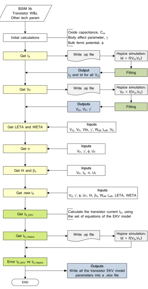
Figure 3.5: Transistor Ids error between EKV model and simulation (HSPICE) results... 64
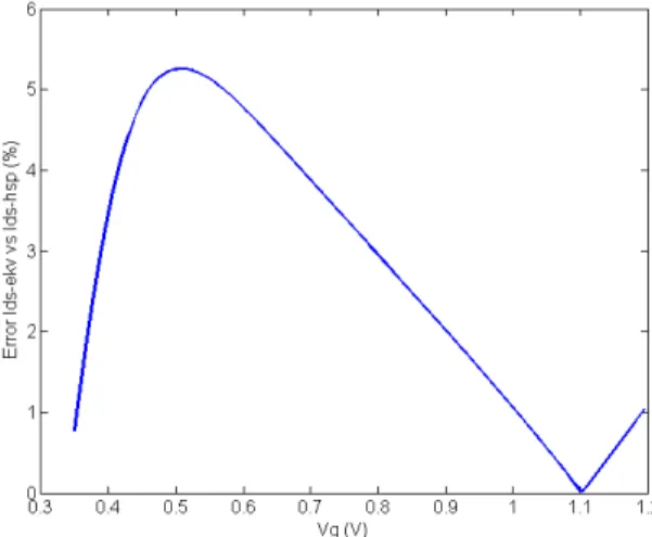
Figure 3.6: Ids error between EKV model and simulation (HSPICE) results for L=const and W=variable ... 65
Figure 3.7: Ids error between EKV model and simulation (HSPICE) results for L= variable and W=const. ... 66
Figure 3.8: Ids error between EKV model and simulation (HSPICE) results for L and W variable ... 67
Figure 3.9: CMOS Varactor ... 68
Figure 3.10: Tuning characteristics for a PMOS capacitor (B=D=S) ... 68
Figure 3.11: PMOS varactor ... 69
Figure 3.12: Tuning characteristics for an I-MOS varactor [39] ... 69
Figure 3.13: Tuning characteristics for an A-MOS varactor [39] ... 70
Figure 3.14: MOS transistor capacitances ... 71
List of Figures
xviii
Figure 3.16: Overview of the several ways to develop electrical models for circuit simulators
[47] ... 74
Figure 4.1: The photomicrograph of an LC-VCO [51] ... 78
Figure 4.2: Integrated spiral inductor: a) Planar inductor simple-π model, b) Single metal layer topology ... 79
Figure 4.3: Integrated spiral inductor: a) modified model [57], b) substrate coupled model [59] ... 80
Figure 4.4: Comparison between complexity vs accuracy of different inductor models ... 80
Figure 4.5: Layout parameters of a square inductor ... 81
Figure 4.6: Inductor behaviour vs frequency ... 86
Figure 4.7: One port π model circuit: a) One port π model, b) One port equivalent circuit .... 86
Figure 4.8: Square planar inductor ... 88
Figure 4.9: Spiral inductor inductance, π model vs ASITIC ... 89
Figure 4.10: Spiral inductor resistance, π model vs ASITIC ... 89
Figure 4.11: Spiral inductor reactance, π model vs ASITIC ... 89
Figure 4.12: Spiral inductor quality factor, π model vs ASITIC ... 90
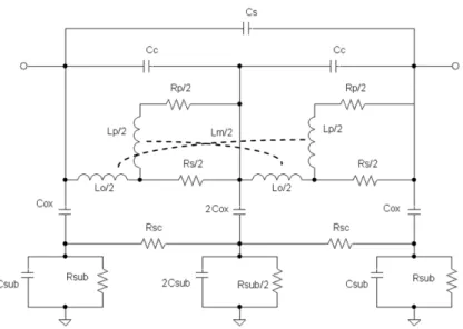
Figure 4.13: Inductor double-π model equivalent circuit ... 91
Figure 4.14: Cross section of a planar inductor ... 91
Figure 4.15: The basic metal-oxide-silicon structure and its equivalent circuit. ... 93
Figure 4.16: 2 GHz Spiral inductor inductance, double-π model vs ASITIC ... 96
Figure 4.17: 2 GHz Spiral inductor quality factor, double-π model vs ASITIC ... 96
Figure 4.18: 6 GHz Spiral inductor inductance, double-π model vs ASITIC ... 96
Figure 4.19: 6 GHz Spiral inductor quality factor, double-π model vs ASITIC ... 97
Figure 5.1: LC tank circuit ... 100
Figure 5.2: Optimization methods ... 105
Figure 5.3: Stochastic search methods ... 106
Figure 5.4: Genetic Algorithm procedure flowchart... 108
Figure 5.5: Particle Swarm Optimization procedure flowchart... 108
Figure 5.6: Layout of a square inductor ... 110
Figure 5.7: General architecture for an optimization design approach... 112
Figure 5.8: Basic Genetic Algorithm Optimization Flowchart ... 113
Figure 5.9: Inductance and quality factor for the designed Inductor ... 120
Figure 5.10: Inductance in the vicinity of the designed Inductor ... 120
Figure 5.11: Quality factor in the vicinity of the designed Inductor ... 121
Figure 5.12: Process variables impact on inductor quality factor and inductance ... 122
Figure 5.14: NMOS inversion-mode varactor ... 125
Figure 5.15: Varactor optimization-based design flowchart ... 126
List of Figures
Figure 6.1: Circuit schematic of an LC-VCO ... 132
Figure 6.2: Double-switch LC-VCO with a current source ... 133
Figure 6.3: Double-switch LC-VCO with parasitic elements ... 135
Figure 6.4: Flowchart of the LC-VCO design tool ... 137
Figure 6.5: LC-VCO optimization design flowchart ... 138
Figure 6.6: LC-VCO design: Optimization Approach ... 140
Figure 6.7: LC-VCO output signal (Vout1 and Vout2) @ 1.0 GHz ... 144
Figure 6.8: Phase noise evolution through each generation ... 145
Figure 6.9: Oscillation frequency evolution through each generation ... 146
Figure 6.10: LC-VCO output signal (Vout1 and Vout2) @ 1.5 GHz ... 147
Figure 6.11: LC-VCO output signal (Vout1 and Vout2) @ 2.0 GHz ... 148
Figure 6.12: LC-VCO output signal (Vout1 and Vout2) @ 2.4 GHz ... 150
Figure 6.13: LC-VCO output signal (Vout1 and Vout2) @ 2.8 GHz ...151
Figure 6.14: LC-VCO output signal (Vout1 and Vout2) @ 1.0 GHz ... 153
Figure 6.15: LC-VCO output signal (Vout1 and Vout2) @ 2.0 GHz... 155
Figure 6.16: LC-VCO output signal (Vout1 and Vout2) @ 2.8 GHz ... 156
Figure 6.17: LC-VCO output signal (Vout1 and Vout2) @ 1.0 GHz ... 159
Figure 6.18: LC-VCO output signal (Vout1 and Vout2) @ 2.0 GHz... 160
List of Tables
Table 1.1: VCO design specifications for RF applications ... 33
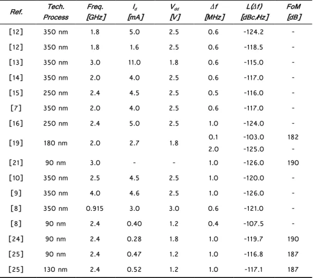
Table 2.1: Published VCO’s characteristics ... 54
Table 3.1: EKV model parameters (L=0.39µm and W=50L) ... 63
Table 4.1: Integrated inductor layout parameters ... 81
Table 4.2: Modified Wheeler Formula coefficients ... 82
Table 4.3: Data Fitted Monomial Expression coefficients ... 83
Table 4.4: Current Sheet Approximation coefficients ... 83
Table 4.5: Square planar inductor dimensions ... 88
Table 4.6: Square planar inductor dimensions (4 nH @ 2-6 GHz)... 95
Table 5.1: Simulation and equation-based optimization ... 103
Table 5.2: Comparison between simulation and equation-based approaches ... 104
Table 5.3: Physical parameters of inductor design ...114
Table 5.4: Design constraints ...115
Table 5.5: Optimization results for minimum tolerance ...116
Table 5.6: Final inductance and % error for several solutions ...116
Table 5.7: Final results for minimum tolerance with discrete-variable optimization ...117
Table 5.8: Comparison of results between evaluated and simulated ...117
Table 5.9: Optimization results for maximum Q ...117
Table 5.10: Final inductance and % error for several solutions ...117
Table 5.11: Final results for minimum tolerance with discrete-variable optimization ...118
Table 5.12: Comparison of results between evaluated and simulated ...118
Table 5.13: Optimization results for a square inductor of 5 nH (Dout max of 200 µm) and its comparison with ASITIC simulations ...119
List of Tables
xxii
List of Tables
List of Symbols
Θ Mobility reduction coefficient
γ Body effect parameter
φ Bulk Fermi potential
σ Metal conductivity
δ Skin depth in AC currents (skin effect)
γ’ Corrected body effect parameter
β0 Transconductance - EKV transistor model parameter
ε0 Permittivity of free space
µ0 Magnetic permeability of vacuum
εr Relative permittivity of silicon
σsi Inductor substrate conductivity
CDB CMOS transistor drain-bulk capacitance
Cextrinsic CMOS transistor extrinsic capacitances
CGB CMOS transistor gate-bulk capacitance
CGD CMOS transistor gate-drain capacitance
CGS CMOS transistor gate-source capacitance
Cif CMOS transistor inner fringing capacitance
Cof CMOS transistor outer fringing capacitance
List of Symbols
xxvi
Cox CMOS transistor gate-oxide capacitance
Cox Inductor metal track - substrate capacitance
Cs Inductor capacitance between metal tracks and underpass
CSB CMOS transistor source-bulk capacitance
Csi Inductor substrate capacitance
din Inductor inner diameter
dout Inductor outer diameter
f Oscillation frequency
gactive CMOS transistors conductance
Gsi Inductor substrate conductance per unit area
gtank Tank resonator conductance
hsi Inductor substrate height
Ids CMOS transistor current through drain to source
if CMOS transistor forward current
Ifor CMOS transistor normalized forward current
ir CMOS transistor reverse current
Irev CMOS transistor normalized reverse current
Is CMOS transistor specific current
l Inductor track length
L{∆f} Phase noise at a frequency ∆fin the vicinity off
Leff CMOS transistor effective length
LETA CMOS transistor short channel effect coefficients
Ls Inductor DC inductance
n Slope factor - EKV transistor model parameter
Q Quality factor
Rs Inductor DC resistance
Rsi Inductor substrate resistance
List of Symbols
Tox CMOS transistor oxide thickness
TR Tuning range
UT CMOS transistor thermal voltage
Vbulk CMOS transistor bulk voltage
Vd CMOS transistor drain voltage
Vg CMOS transistor gate voltage
Vg’ Corrected CMOS transistor effective gate voltage
VP CMOS transistor pinch-off voltage
VP’ Corrected CMOS transistor pinch-off voltage
Vs CMOS transistor source voltage
Vt0 CMOS transistor threshold voltage
Vtank Oscillator output voltage amplitude
w Inductor track width
Weff CMOS transistor effective width
Acronyms
ACM Area Calculation Method - transistor model
BiCMOS Bipolar Complementary Metal Oxide Semiconductor
BJT Bipolar Junction Transistor
CAD Computer-Aided Design
CMOS Complementary Metal-Oxide-Semiconductor
EA Evolutionary Algorithms
EKV Enz, Krummenacher and Vittoz - transistor model
EM Electromagnetic simulator
FoM Figure of Merit
GA Genetic Algorithms
gm Transistor transconductance
GNP Graphical Nonlinear Programming
HSPICE Hailey Simulation Program with Integrated Circuit Emphasis
MGA Modified Genetic Algorithms
NMOS N-type Metal-Oxide Semiconductor
PMOS P-type Metal-Oxide Semiconductor
PN Phase Noise
PSO Particle Swarm Optimization
Acronyms
xxx
SPICE Simulation Program with Integrated Circuit Emphasis
SQP Sequential Quadratic Programming
UMC130 United Microelectronics Corporation – 130 nm
Varactor Variable capacitor
VCO Voltage Controlled Oscillator
VHDL-AMS Very High speed hardware Description Language - Analog and Mixed-Signal
1
Introduction
This chapter emphasizes the main issues addressed in this thesis. The chapter starts presenting the motivation that has lead to this work, and briefly gives an overview regarding
the background on the subject. Issues that are still open concerning analog/RF design
meth-odology are offered, as the base for the proposed research question. The expected and achieved contributions resulting from this work are presented. Finally, the chapter gives a de-scription of this thesis organization.
1.1
Motivation and Background
The worldwide market of communications systems circuits, such as clock generation, frequency synthesizers or timing-recovery circuits, is still growing exponentially. The demands for new communications services have motivated manufacturers competitiveness in order to provide equipments with higher performance and lower cost, than the previous generation. In fact, and assuming the prediction in [1], during the first decade of the XXI century, the goal for this market was to reduce both the power consumption and price of this devices by 30% every year. This demand has been pulled up, but not only, by the advances in wireless tech-nology that brought to mobile devices the challenge of incorporating in the same equipment a set of functionalities such as text, audio, video, web access, global position system (GPS) or smart handheld devices.
As result of the progress in technology development and the use of submicron CMOS processes, digital circuits have become faster and more precise, and with decreased of the implementation area. This technological improvement enforces more restricted specifications in
terms of gain, phase noise and size for the analog/RF counterparts. Consequently, the design
of analog/RF devices becomes more challenging, as recent technologies carry two major
Introduction
32
the challenge of analog/RF design task nowadays is to design a circuit to accomplish the
required specifications, at low supply voltage, (for low power consumption) and low phase noise, taken into account that transistors have more parasitic effects and less intrinsic gain. Moreover, the performance of an on-chip device is aimed to get closer to those achieved with an off-chip device. Therefore, there’s a question that always climbs at a designer’s mind, “How to size analog circuits to achieve the required performances?” [2].
In the particular case of RF systems, such as a receiver or a transceiver, RF circuits
must process analog signals with a wide dynamic range at high frequencies, and the voltage
controlled oscillator (VCO) is a critical element in the RF front-end block. The trade-off
be-tween phase noise, oscillation frequency and power consumption are particularly demanding when aiming a fully integrated solution. The trade-offs involved in the design of such circuits can be summarised in Figure 1.1.
Figure 1.1: VCO design trade-offs
The wide variety of VCO applications in communications systems, working from some hundreds of MHz up to a few GHz, and motivated by the fact that transistors size have been scaled down, has lead to the full integration of the VCO in a chip. From manufacturers’ point
of view, this new market demand is characterised by the Price-Package-Performance-Power,
usually called as the P words.
An oscillator can be defined as a device that generates a periodically time-varying
sig-nal. There are various forms of oscillator implementations, such as ring, LC tuned, crystal and
Introduction
Table 1.1: VCO design specifications for RF applications Specification Unit
Centre Frequency GHz Tuning Range MHz
Phase Noise dBc/Hz @ offset [kHz] Power consumption mW
Supply voltage V
VCO gain MHz/V
Pullling MHz/load-specif.
Pushing MHz/V
Area µm2
Cost €
Operating Temperature ºC Manufacturability
Yield %
Lifetime Years
Regarding the implementation of a fully integrated VCO, the usual choice goes to the
ring, relaxation or LC oscillators. The first two, have a wide tuning range when compared with
LC oscillators, as well as lower implementation area. However, LC oscillator shows better
per-formance concerning phase noise and power consumption. Due to this, in those applications where lowest possible phase noise with low power dissipation is the driving issue, designers
may decide to use LC oscillators [4]. Hence, they are extremely popular in RF applications.
The frequency of most RF oscillators must be adjustable. For that purpose, oscillators
can be controlled either by voltage (called voltage controlled oscillators) or by current. Al-though current controlled oscillators are feasible, they are not used often due to difficulties in
controlling the energy stored in the LC tank by current. Several topologies have been
pro-posed in literature for VCOs implementation. The two most popular topologies are the Colpitts
or the negative Gm oscillators, as they provide a negative resistance through a feedback loop,
in order to reduce the losses in the circuit, consequently attaining better performance [5]. These topologies can be implemented either with bipolar or MOS transistors [4]. In this work, only the MOS version is considered, since CMOS technology is preferable for this category of circuits, due to their better performance with digital circuits, and less power dissipation when compared with BJT technology. Furthermore, due to their simplicity, CMOS oscillators based
on controlling the negative Gm are the designers’ first choice.
LC-voltage controlled oscillators (LC-VCOs) can also have single or differential output.
For RF oscillators the differential output is preferable since their common mode rejection
char-acteristic provides better immunity to some noise sources. In Figure 1.2 and Figure 1.3 four
Introduction
34
a) Current source to ground b) Current source to Vdd Figure 1.2: NMOS LC-VCO
The NMOS structure in Figure 1.2a has the smallest sensitivity to noise on the ground
level, however suffers from pushing, due to the high sensitivity to noise coming from power
supply. On the other hand, this topology has a lower flicker noise, than those with current source to the supply represented in Figure 1.2b [3]. Moreover, as the inductors are con-nected to the supply voltage, both structures can achieve an output signal swing twice the power supply voltage. This feature can lead to a phase noise reduction, since noise is strongly dependent on the oscillation amplitude.
In the same way, the structures shown in Figure 1.2 can be implemented using PMOS transistor. Although for carrying the same current, and because PMOS are not as fast as NMOS, typically the width increases by a factor of 2-3 (consequently, large implementation area), they are less vulnerable to flicker noise as the Bulk terminal is connected to the source (assuming an ideal power source).
There is a possibility to combine NMOS and PMOS in the structure, taking advantage of the best performance of each one, obtaining the topology represented in Figure 1.3. This type of structure has as main advantage the reduction of the power consumption to half when compared to those in Figure 1.2. The choice about where to place the current source depends on whether our concern is to make to oscillator less sensitive to ground or to power supply levels. The circuits shown before share the basic concept of providing a negative resistance in opposition to that in the tank, so that the overall losses are reduced. Moreover, this negative
resistance will also improve the “quality” of the oscillator, since the average power dissipated
is reduced.
Introduction
c) Current source to ground d) Current source to Vdd Figure 1.3: Double switch LC-VCO
Although analog/RF design is not a new topic, the state of the art regarding analog
considers [2]:
− There is no universal approach for analog design. The design methodology is usually
based in designers experience and previous knowledge. Sometimes, the try-and-see design, supported by simulations, is still used.
− A large number of CAD tools are offered, mostly for simulation and layout generation
of analog circuits.
− A considerable number of analog design automation tools have been proposed by
Academia. However, these tools suffer from the lack of a common approach and de-sign methodology, and usually are not adopted by the industry. On the other hand, digital design automation tools are quite well accepted by designers.
As a result, and supporting the motivation for this work, there still exist a few number of
issues that to be taken into account, and does not have an unanimous answer among de-signers, such as:
− As technology is scaling down, how to deal with both increasing complexity of
ana-log/RF circuits, and the ever more stringent specification?
− Is it possible to design an analog/RF device, through optimization procedures, and
still attaining to the best design trade-offs?
Introduction
36
− Is it possible to shorten the design time for hand-calculations and
elec-tric/electromagnetic simulations?
− Is there any benefit in going firstly through an optimization-based design and then to
a final simulation, rather than to a full simulation-based design?
− How to give designers the possibility of being aware about device physics impact in
circuit performance, and at the same time take them it into account in the design process?
− Is it preferable to have an accurate design based on blind believing simulators,
rather than a less accurate design but in which it is possible to get a deep knowl-edge concerning the device behaviour?
These are just some of the questions that, probably, a designer holds in his mind.
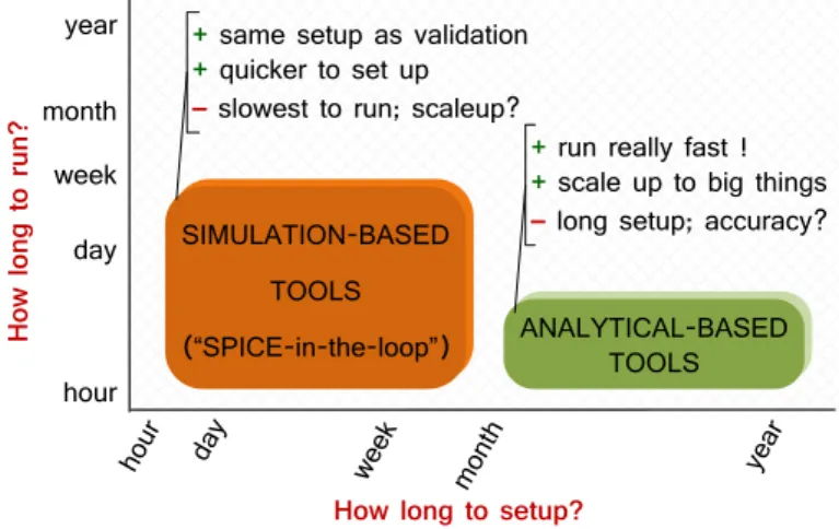
Summarizing, the above issues highlight the traoff between design accuracy and de-sign time. If, on one hand, the requirement to provide useful insight into circuit behaviour, si-multaneously with the necessity for circuit correction, makes prohibitive the use of numerical optimizers or fully automated CAD tools; on the other hand, analytical-based systems, usually, run faster, are able to deal with complex circuit design, and are easily adaptable to new “re-alities”, such as new technology processes, among others. In Figure 1.4, a qualitative com-parison between simulation-based and analytical-based design tools is depicted. With today’s electric/electromagnetic simulators, the effort to simulate a specific circuit mostly depends on the circuit design level, i.e., if it is a circuit description level or a physical description level. In
the particular case of LC-VCO several hours may be needed to perform a single simulation.
Analytical-based design tools are known for being fast in characterizing the circuit behaviour; however, generally, it takes a long time to setup.
SIMULATION-BASED TOOLS
(“SPICE-in-the-loop”) ANALYTICAL-BASEDTOOLS hour
day week month year
hour day week
month year
How long to setup?
How long to run?
+ same setup as validation
+ quicker to set up – slowest to run; scaleup?
+ run really fast !
+ scale up to big things – long setup; accuracy?
Figure 1.4: Analog Design characteristics: simulation vs analytical tools
Introduction
1.2
Problem Formulation
When designers have in hands the task of designing a VCO, one of the main chal-lenges is to obtain results between simulation and on-chip measurement as close as possible. For this propose, it is essential to have accurate models for each of the circuit blocks.
As aforementioned a VCO should provide a signal within a certain frequency as pure as possible and which can be adjusted by external voltage. As can be seen in Figure 1.3
(sec-tion 1.1), a VCO has two main blocks; the LC tank responsible for the oscillation frequency,
and the active circuit which is responsible for reducing the circuit losses introducing a negative
resistance. Most of the LC-VCO designs have as main criteria to achieve both minimum
phase noise and minimum power consumption for a certain oscillation frequency and desired tuning range. In a very simplistic point of view, for a specified frequency and tuning range (and maximum phase noise), the design problem to be worked out is the sizing of all the
elements of the LC-VCO. As the correlation among the design variables is very strong, this
has yielded in a large number of design methodologies has being proposed in the literature, as will be presented in chapter 2. Notwithstanding, a brief introduction can be offered at this point. The type of approach followed could be the key for the success of the design in
achieving the best solution. In order to design a full LC-VCO, designers must take into
ac-count the following components’ parameters:
− Inductance value, L, and its parasitics;
− Capacitor capacitance, C, and parasitic resistance;
− MOS transistor: characterisation, technology, parasitics, models, ...
Most of the bibliography focuses the design of the LC-VCO in the trade-off between
phase noise and power consumption. The main issue focused, concerns the design of circuits with low current consumption without phase noise degradation.
In [7] a complete description of a design of integrated LC-VCOs is presented, where
the complexity of the optimization design, regarding the number of variables involved, is
fo-cused. The design of a fully on-chip LC-VCO requires simultaneous optimization of multiple
variables, where the major difficulty is to estimate the losses on-chip, mainly due to the induc-tor, which gives to the on-chip circuit a worst performance than that obtained for an off-chip circuit. The use of computer-aided optimization is essential to find the optimum design in such a complex circuit. Although, this sometimes is understood as to limit the designers’ sensibility to the trade-offs among the parameters involved, as the result achieved is copiously reliant on optimization process. To overcome the mentioned drawback, a graphical optimization
method-ology which uses graphical nonlinear programming (GNP) is proposed [7]. With GNP,
Introduction
38
intuitions in finding the optimum solution. The optimization process can be summarized in three main steps as following:
− The tail current in the oscillator must be set to Imax. The drain current in each
tran-sistor is the dominant contributor to the phase noise;
− The inductor inductance must be fixed, and an inductor that minimizes the losses
should be chosen. The inductor is the element responsible for the most of the losses, so as higher the losses, smaller is the design space;
− For the selected inductor, the optimization process is evaluated taking into account
the design constraints. If a practicable design point is achieved, a new optimization process is evaluated for a lower inductance value.
− This procedure is repeated until the design space (2D design space) is reduced to a
single point, the optimum design.
The optimization methodology presented before, is just one from an extensive range of different methods adopted for the oscillator design that can be found in the literature. A few more examples will be briefly referred as following:
− In [8], Matlab, Cadence SpectreRF and ASITIC are used. Here, the LC-VCO design
optimization is based on the gm/ID methodology, where the oscillator design space is
studied with the goal of choosing the optimum design, considering phase noise – consumption trade-off;
− In [9] a graphical optimization method is presented. In this work, design constraints
are imposed on tuning range, tank voltage amplitude, star-up condition, power con-sumption and phase noise. Those constraints are graphically represented in order to give to the designer an overview of the correlation between design parameters. The results obtained by analytic form are verified with simulation using ADS;
− In [10] for the design optimization a geometric programming method is used. The
geometric program (GP) is a type of mathematical optimization problem character-ized by objective and constraint functions in a special form. Here, Matlab was used for solving the convex form of a GP. The design constraints mentioned in the previ-ous work, were also considered in this work.
As mentioned, the design and optimization process of and LC-VCO can be very
di-verse. The type of application for the oscillator, CMOS technology used, models’ complexity …
are just few of the points that make the design and optimization of a fully integrated LC-VCO
Introduction
As a final remark regarding any LC-VCO optimization process is that it ought not to be
seen as the final design, and subsequent simulation must be done in order to tune the design to comply with the desired specifications.
1.2.1
Research Question
This work aims to develop a tool to support the design of an LC-VCO oscillator. Under the
umbrella of such a broad subject, the following sentence spotlights the research question of this work.
Would evolutionary algorithms be capable of improving the performance
and achieve the best design solution of an LC-VCO optimization process, that
ought to take into account accurate models of each component, as well as to be adaptable to technology changes and take into account technology/design constrains.
1.3
Contributions
This research has spotlighted the optimization based design of LC voltage controlled
oscillators, by means of evolutionary algorithms. Such design involves some design trade-offs and relies on the estimation of several correlated parameters, consequently, traditional hand-calculation methods are not an option when CMOS submicrometer technology is being used. On the other hand, simulation based optimization, which is generally the most accurate design procedure, usually is an extremely time consuming process and can become prohibitive if fast
design, or at least a fast first design approach, is desired.
To achieve the goal proposed for this thesis, the early chapters emphasis is placed on finding the most suitable analytical models that characterize with good accuracy the behaviour of each single element in the circuit: the CMOS transistor, the inductor and the varactor. These models, which must rely on technological parameters, in opposition to those based in fitting parameters supported by an exhaustive simulation process, are a fundamental key for an optimization based design procedure, that aims to be simulation independent. Such kind of analytical models, allows to understand the device physics and to apply it successfully for the
analog/RF design purposes.
Introduction
40
As a final remark, it will be shown that the performance of the LC voltage controlled
oscillator, designed by the proposed optimization-based design tool, gives fairly acceptable results when compared with those obtained through commercial simulators. It proves that the proposed tool is a good design instrument for a first approach design, as intended to be.
The following book chapters, journal and conference publications have resulted from the work presented in this thesis:
• Pereira, P., H. Fino, F. Coito, and M. Ventim-Neves, "ADISI- An efficient tool for the automatic design of integrated spiral inductors", IEEE International Confer-ence on Electronics, Circuits, and Systems (ICECS), pp. 799–802, December, 2009.
This work introduces a tool for the optimization of CMOS integrated spiral inductors. The core of the tool is an optimization-based methodology where technology constraints on the inductor layout parameters are considered by applying user-defined discretization on the design variables. This is particularly important since it enables the generation of the best solu-tion for the technology used. Further constraints imposing predefined relasolu-tion between layout
parameters are also considered as a way of implementing heuristic design rules. The trade-off
between quality factor and device area is evaluated through the generation of a graphical rep-resentation of quality factor versus output diameter for a given inductance. For the sake of
simplicity the π-model has been used for characterising the inductor. The validity of the design
results obtained is checked against circuit simulation with ASITIC. The main limitation of the work proposed resides in the applicability of the tool to higher frequencies. This limitation is
inherent to the π-model used for the integrated inductor, which is valid for frequencies lower
than 1GHz.
• Pereira, P., M. H. Fino, and F. V. Coito, "Using discrete-variable optimization for
CMOS spiral inductor design", International Conference on Microelectronics (ICM), pp. 324–327, December, 2009.
In this paper a discrete-variable optimization methodology for the automatic design of CMOS integrated spiral inductors is proposed. The use of discrete variable optimization proce-dure offers the designer the possibility for exploring the design space exclusively in those points available for the technology under use. A comparison between using discrete-variable optimization and a continuous optimization procedure followed by a discretization of the results is presented, where the benefits of the proposed methodology are presented. In all examples the discrete–variable optimization proved to be better.
Introduction
Conference on Computing, Electrical and Industrial Systems (DoCEIS), pp. 515-522, February, 2010.
The main objective of the optimization based tool presented in this work, is to generate the geometrical layout parameters of integrated spiral inductors. For this purpose two main concerns were considered. On one hand, a Genetic Algorithm (GA) optimization procedure where a technology-aware methodology is adopted, and the discrete nature of the variables is also accounted for as a way of restricting the search space to those points allowed by the technology. Furthermore, GAs do not require derivative information or previous knowledge, as well as the algorithm determines global optimum solutions, avoiding getting trapped in local maximum/minimum, as frequently happen with continuous variable optimization algorithms. On the other hand the necessity for obtaining solutions in an efficient way led to the use of the inductor physical model, instead of using a simulation based approach. The Matlab GA tool-box is used, and some GA functions were added, yielding technology feasible solutions is
presented. For the sake of efficiency and simplicity the π-model is used for characterizing the
inductor.
• Pereira, P., M. H. Fino, and M. Ventim-Neves, "Automatic generation of RF inte-grated inductors analytical characterization", International Workshop on Symbolic and Numerical Methods, Modeling and Applications to Circuit Design (SM2ACD), pp. 1-4, October, 2010.
This paper addresses the automatic generation of RF integrated inductors model for
wider frequency range. In this work the double π-model is used as a way of characterizing the
inductor behaviour for frequencies above the 1.0 GHz. The double π-model is supported by a
set of equations based exclusively in technology parameters instead of equations obtained by fitting process of measure data. The main advantages of the tool presented in this work when compared to using an electromagnetic simulator reside not only in the computation time but also in the possibility for being fully integrated into an optimization based design tool. The use of a technology-based methodology for the evaluation of the model parameters grants the adaptability of the models generated to any technology.
• Pereira, P., M. Helena Fino, F. Coito, and M. Ventim-Neves, "RF integrated in-ductor modeling and its application to optimization-based design", Analog Inte-grated Circuits and Signal Processing, vol. 73, issue 1: Springer Netherlands, pp. 47-55, 2011.
In this work an optimization-based approach for the design of RF integrated inductors is
addressed. For the characterisation of the inductor behaviour the double π-model is used. The
Introduction
42
straightforward. The inductor analytical characterization is integrated into an optimization-based
tool for the automatic design of RF integrated inductors. This tool uses a Modified Genetic
Algorithm (MGA) optimization procedure, where user defined constraints on the design pa-rameters are taken into account. This tool allows overcoming the typical limitation of most non-commercial tools, such as ASITIC, regarding their impossibility for being integrated into an optimization loop.
• Pereira, P., H. Fino, F. Coito, and M. Ventim-Neves, "Optimization-Based Design of Nano-CMOS LC-VCOs", Doctoral Conference on Computing, Electrical and In-dustrial Systems (DoCEIS), pp. 453-464, February, 2012.
This paper introduces a variability-aware methodology for the design of LC-VCOs in Nano-CMOS technologies. The complexity of the design as well as the necessity for having an environment offering the possibility for exploring design trade-offs has led to the develop-ment of design methodologies based multi-objective optimization procedures yielding the gen-eration of Pareto-optimal surfaces. The efficiency of the process is granted by using analytical models for both passive and active devices. Although physics-based analytical expressions have been proposed for the evaluation of the lumped elements, the variability of the process parameters is usually ignored due to the difficulty to formalize it into an optimization perform-ance index. The usually adopted methodology of considering only optimum solutions for the Pareto surface, may lead to pruning quasi-optimal solutions that may prove to be better, should their sensitivity to process parameter variation be accounted for. In this work we pro-pose starting by generating an extended Pareto surface where both optimum and quasi-optimum solutions are considered. Finally information on the sensitivity to process parameter variations, is used for electing the best design solution.
• Pereira, P., H. Fino, and M. Ventim-Neves, "RF Varactor Design Based on Evo-lutionary Algorithms", International Conference on Mixed Design of Integrated Cir-cuits and Systems (MIXDES), pp. 277-282, May, 2012.
This paper introduces an optimization methodology for the design of RF varactors. The
Introduction
• Pereira, P., A. Sallem, M. Fakhfakh, M. H. Fino, and F. Coito, "A
Technology-Aware Optimization of RF Integrated Inductors", Analog Circuits: Applications, Design and Performance: Nova Science Publishers, Inc., pp. 213-234, February, 2012.
This book chapter presented the optimal design of RF integrated spiral inductors,
through the use of Particle Swarm Optimization (PSO), as an alternative to genetic algorithms optimization. The efficiency of the design process is granted by using an analytical model to
characterize integrated inductors based on the double π-model. Physically-based equations for
the evaluation of the model parameters are considered, as a way of easily adopting the model to any new technology. PSO is used to generate optimal values of parameters of the devel-oped models. Several working examples for mono-objective and multi-objective optimization were considered. The viability of the obtained design solutions is highlighted via comparison with ASITIC simulation results.
• Coito, F., H. Fino, and P. Pereira, "Variability-Aware Optimization of RF
Inte-grated Inductors in Nanometer-Scale Technologies", InteInte-grated Circuits for Analog Signal Processing, New York, Springer-Verlag, pp. 271-288, 2012.
A multi-objective optimization based methodology for the design of integrated inductors is addressed in this book chapter. The necessity for obtaining design solutions robust against the technological parameters variability has led to a new methodology where an extended-Pareto surface is generated. This extended-extended-Pareto front contains both optima solutions and quasi-optimum solutions. Finally information on the robustness against process parameter variations is used for electing the best design solutions.
• Pereira, P., H. Fino, and M. Ventim-Neves, "LC-VCO design methodology based on evolutionary algorithms", International Conference on Synthesis, Modeling, Analysis and Simulation Methods and Applications to Circuit Design (SMACD), pp. 189-192, September, 2012.
This paper introduces an LC-VCO design methodology based on evolutionary
Introduction
44
• Pereira, P., M. Helena Fino, and M. Ventim-Neves, [Invited article based on
"LC-VCO Design Methodology Based on Evolutionary Algorithms" – SMACD 2012], Analog Integrated Circuits and Signal Processing, Springer Netherlands,
pp., 2013. – To be published
This article is an extended document based on the previous work, where a more
de-tailed explanation regarding the LC-VCO design methodology based on evolutionary
algo-rithms, is offered.
• P. Pereira, H. Fino, M. Fakhfakh, F. Coito, M. Ventim-Neves, "LC-VCO Design
Challenges in the Nano-Era", Analog/RF and Mixed-Signal Circuit Systematic
Design, vol. 233, Springer Berlin Heidelberg, pp. 363-379, 2013.
This book chapter, put together some of the previous publications, and gives a full
overview regarding the complexity of designing LC-VCOs, which has lead to the development
of several design methodologies. The design of LC-VCO is supported by a Genetic Algorithms optimization methodology, which is able to deal with both continuous and discrete variables, making possible to satisfy both technological and layout constraints, proposed in early works, is presented in this chapter. A set of design examples showing the design of three VCOs for different oscillation frequencies were considered. The feasibility of the obtained design solu-tions is highlighted via comparison with simulated results.
1.3.1
Other Related Publications
In parallel with the present work, a few other publications regarding similar lines of re-search were also possible due to a fruitful collaboration with their co-authors.
• Pereira, P., F. Coito, and H. Fino, "PSO-Based Design of RF Integrated Induc-tor", Doctoral Conference on Computing, Electrical and Industrial Systems (Do-CEIS, pp. 475-482, February, 2012.
• Sallem, A., P. Pereira, M. Fakhfakh, and H. Fino, "A Multi-objective Simulation
Based Tool: Application to the Design of High Performance LC-VCOs",
Techno-logical Innovation for the Internet of Things, vol. 394, Portugal, Springer Berlin Heidelberg, pp. 459-468, 2013.
• P. Pereira, M. Kotti, H. Fino and M. Fakhfakh, “Metaheuristic Algorithms Compa-raison for the LC-Voltage Controlled Oscillators Optimal Design”, The 4th IEEE TN CEDA’s ENG-OPTIM’ Contest: ‘‘Engineering Applications of Optimization
Introduction
1.4
Chapter by Chapter Overview
The remainder of the thesis is organized as follows: Chapter 2 describes in more detail
the background of the work developed, in particular the analog/RF design methodology and
strategy applied to LC voltage controlled oscillators. A special attention will be given to
ana-log/RF design tools based in analytical models, instead of simulation-based design tools.
Chapter 3 introduces the EKV MOS transistor model as the path for the accurate characteri-zation of the transistor behaviour. The CMOS transistor has been widely used, not only as an active element, but also as a passive device, in the figure of a varactor. Chapter 4 presents the planar spiral inductor. Moreover, accurate and technological dependent analytical models are identified, aiming its inclusion in an optimization-based design procedure. The optimal de-sign of radio-frequency integrated spiral inductors and capacitors, supported by means of evo-lutionary algorithms, is presented in Chapter 5, while Chapter 6 addresses the optimal design
of a full LC voltage controlled oscillator, taking into consideration circuit specifications and
2
Background on VCO Design and
Optimization Methodologies
In this chapter the background information necessary for the understanding of several
key aspects regarding the design and optimization methodologies of LC-oscillator circuits is
addressed. Firstly, a general overview concerning the design of analog/RF circuits is
pre-sented. Afterwards, a more detailed analysis is devoted to the techniques adopted by different
authors, aiming the full design of an LC voltage controlled oscillator.
2.1
Introduction
Analog/RF design still is a knowledge-based design. Somehow, analog/RF design is
based partially in the designer’s knowledge, a portion of designer’s intuition, the designer qualitative analysis, and suffers from the lack of design formalism. Even though, in a certain
part of the design process, there is place for a formal mathematical approach, the analog/RF
design can be contrasted with its counterpart, the digital design, in terms of design process, whereas digital design has, usually, straightforward design techniques.
It is usual to say that analog/RF design is more a form of art and less science. Since
it relies in an intensive knowledge, is a multiphase and iterative task, and, consequently, it
goes for a substantial period of time [11]. The absence of an analog/RF circuit design
for-malism stems from the nonexistence of a circuit-independent design procedure and the lack of a formal representation, which allows a proper formalization of the problem. The nature of the analog signals that the device deals with, as well as it time dependency, is considered to be
the main cause for the difficulty in achieving a structured problem representation. In the
bibli-ography, the proposed techniques needed to produce successful analog/RF devices are
Background on VCO Design and Optimization Methodologies
48
Notwithstanding, analog/RF design tools can provide initial candidate solutions, which
can be seen as a starting point for a final design. In the last decade, there have been a ‘boom’ in analog tools, aiming to help designers in obtaining an accurate design, providing an initial and fairly precise solution that can be applied to formal tools, e.g. electromagnetic simu-lators. The nature of continuous signals domain in analog circuits, requiring the application of
calculus, is in general costly in terms of complexity. Yet, the problem can be simplified if
con-verted to a discrete problem domain, which is liable to be included in a logical structured problem, offering an approximation to a final design solution. These issues, allied to the de-mand for smaller device sizes and higher scales of integration, climbs up a few steps in circuit design complexity.
Generally, the accuracy to which analog/RF design are devoted to, simultaneously with
the rising need for analog/RF system simulation, makes the design time for analog/RF
cir-cuits the bottleneck of any analog design. Even though 90% of an integrated circuit may pos-sibly be digital and only 10% reserved for analog, most of the design time and endeavour is dedicated to the analog part [11]. Moreover, the design of digital circuits is rather fairly sup-ported by computer-aided design tools than its analog counterpart. In Figure 2.1, a qualitative comparison between digital and analog design is depicted.
DESIGN TOOLS
Design Effort (& Complexity)
Design Effort (& Complexity)
DESIGN TOOLS
DIGITAL ANALOG
Design Problem (%)
Figure 2.1: Digital vs analog design
The LC voltage controlled oscillator, as a pure analog circuit, suffers from the same
ad-vantages and drawbacks regarding its design problem formulation, as abovementioned. As result, many have tried to develop analog tools for the design, layout and characterization of
LC-VCOs, aiming to help analog designers in their effort in achieving the best circuit
perform-ance, compliant with circuit’s specifications.
Background on VCO Design and Optimization Methodologies
2.2
Early Work
The design of LC voltage controlled oscillators implies several different aspects, which
allows saying that it has a long history back to early researches, such as Maxwell, whose laws are applied to magnetic effects.
In recent times, the design and optimization of LC oscillators by means of geometric program was proposed in [12]. The authors stated that the synthesis method is fast, and global optimization design is determined, where the final solution is completely independent of the starting point. The optimization process through geometric program is very efficient, ac-cording to the authors, allowing designer to spend more time exploring design trade-offs rather than sizing the circuit elements, where the design methodology engage twelve variables. From our point of view, the weakest points of the work proposed in [12], are, specially, the analyti-cal models used for the circuit elements characterization. For the inductor characterization Greenhouse’s approach is used, however the model adopted suffers from the lack of accuracy at high frequencies, above 1GHz, whereas for the varactor an ideal capacitor in series with a resistor is considered. A couple of design examples in a standard 0.35µm, 2.5V CMOS proc-ess, where the optimization algorithm deals with a single objective function, the minimization of the oscillator phase noise, are offered. Despite good performance achieved, results valida-tion, at least, against device-level simulations is not presented.
An automated and layout-aware RF LC-VCO design, entitled CYCLONE was offered in
[13]. The proposed tool combines in the design process both the device-level simulation for granting the accuracy of the tool and the advantage of evolutionary algorithms, respectively the simulated annealing algorithm, for the search of the best feasible solution. As a tremen-dous effort is put on the design accuracy, electromagnetic finite-element simulators are used, in particular for the inductor characterization, as its parasitics can easily jeopardize expected performances. In CYCLONE, two electromagnetic simulators are used, increasing the design
process complexity. As result, the design time of the LC-VCO is mainly engrossed by
simula-tions. A few design and layout generation examples for two VCO topologies are shown. A low resistive substrate 0.35µm, 1.8V CMOS process was used.
A design strategy focused in the inductance selection scheme is performed using a
graphical optimization method to optimize the phase noise of a cross-coupled LC-VCO,
sub-jected to design constraints is presented in [14]. The main idea is to obtain graphically a search space, called feasible design regions, based on circuit specifications, as well as design constraints, and then to look forward for the best design solution. The advantage of the method is that it provides physical insight into the space search, allowing designers to adjust the design solution according to their knowledge and experience, which can be seen as a negative aspect. On the other hand, as the highlight was put in the graphical optimization
Background on VCO Design and Optimization Methodologies
50
which bring some inaccuracy to the final design. The LC-VCO design examples shown were
obtained n a 0.35µm, 2.5V CMOS process.
The design of a cross-coupled LC oscillator in a 0.25µm, 2.5V CMOS process,
achiev-ing low phase noise with low power consumption and wide tunachiev-ing range is addressed in [15]. In this work the VCO design methodology is not sustained in computer-aided design tools, but supported in the expertise and intuition of the designers. Yet, the authors provide important information regarding design trade-offs, which are very helpful for being integrated in an opti-mization-based design methodology.
An LC-VCO design and optimization example is shown in [7], where 12 independent
design variables were identified; 4 of them regarding to the transistor dimensions, other 4 re-lated to the geometric parameters of the integrated inductor (metal width, metal space, num-ber of turns, and external diameter), 2 associated to the varactor (maximum and minimum capacitance), the load capacitance, and finally the tail current in the oscillator. A design ex-ample of the design of an LC-VCO for a specified set of specifications (centre frequency, tun-ing range, …) and havtun-ing the phase noise as the objective function, is shown. As a design strategy, aiming to reduce the complexity of the optimization process and, consequently the number of variables, only the dominant sources of noise were considered on the phase noise function, yielding a reduction of 50% on the number of independent variables. The 6 inde-pendent design variables to optimize are: transistors width, varactor maximum capacitance metal space, number of turns, and external diameter from the inductor, and the tail current in
the oscillator. For the optimization design methodology a graphical nonlinear programming
(GNP) is proposed. The use of such methodology can be seen as an intuition-optimization
methodology, since the final design step relies on the designer skills.
A lot of researchers pay attention at phase noise analysis, as well as the different noise
sources, when designing an LC-VCO, since it plays an important role in circuit performance. A
numerical optimization technique based on analytical equations applied to the design of a
cross-coupled differential CMOS LC oscillator is addressed in [16]. According to the authors,
to take the advantage of Leeson’s equations for estimating the circuit phase noise, an
optimi-zation routine was built, using sequential quadratic programming (SQP), which is generally
applied for nonlinear optimization problems. As a strong drawback, this work considers a very simplified tank model, reducing the complexity of the optimization process at the expense of the results accuracy.
Considerable research efforts have been devoted to achieve low phase at minimal
power consumption. Different techniques applied to each component of the LC oscillator, such

![Figure 3.16: Overview of the several ways to develop electrical models for circuit simulators [47]](https://thumb-eu.123doks.com/thumbv2/123dok_br/16572446.738068/74.892.219.630.713.1060/figure-overview-ways-develop-electrical-models-circuit-simulators.webp)
![Figure 4.3: Integrated spiral inductor: a) modified model [57], b) substrate coupled model [59]](https://thumb-eu.123doks.com/thumbv2/123dok_br/16572446.738068/80.892.127.712.133.342/figure-integrated-spiral-inductor-modified-model-substrate-coupled.webp)