ABSTRACT: Carbon nanotubes are possible building blocks in the development of new generation of electronic devices. The carbon nanotubes allow one fabrication of devices using nanometric scales. They can be used in projects of a wide range of electronic and optoelectronic components such as diodes, transistors and interconnection elements, among others. This paper presents the state-of-the-art of this area, emphasizing the inluence of quantum effects on the characteristics of such components.
KEYWORDS: Nanoelectronics, Carbon nanotubes, Nanotransistors.
Nanoelectronic Devices Based on
Carbon Nanotubes
Victor Dmitriev1, Fernando Gomes1, Clerisson Nascimento1
INTRODUCTION
Carbon nanotubes (CNT) with diferent conigurations are the most studied nanomaterials since their discovery in 1991 by S. Iijima (1991). hey present a single hollow cylinder with one or several layers of carbon atoms. he CNTs behave as one-dimensional (1-D) systems since their diameters are on the nanometric scale and are much smaller as compared to their lengths. 1-D nature of CNT deines their special physical properties, which have been used in design of novel electronic devices. It is expected that the nanocomponents based on CNT will have some of electrical and optical parameters far superior than the existing microelectronic components based on Si, Ge or GaAs semiconductors (Dragoman and Dragoman, 2006).
here is a relentless pursuit of getting smaller and smaller devices with low energy consumption and high processing speed in many areas, including aerospace technology. In this sense, single-wall carbon nanotubes (SWCNT) have been very promising because, depending on their chirality and diameter, they may exhibit metal or semiconducting behavior (Yao et al., 1999). his allows one to project good conducting wires and p-n junction in nanometric scale.
In this paper, we present a review of electrical properties of some components based on SWCNT. In particular, interconnecting elements, Schottky diodes and ield-efect transistors are discussed. We make a comparison of the nanoelectronic components based on CNT and the corresponding microelectronic devices and discuss the principal problems in their modelling.
1.Universidade Federal do Pará – Belém/PA – Brazil.
Author for correspondence: Fernando Gomes | Departamento de Engenharia Elétrica, Universidade Federal do Pará | Avenida Augusto Correa, 1 | CEP: 66.075-110 Belém/PA – Brazil | Email: [email protected]
NANOELECTRONIC COMPONENTS
BASED ON
CNT
CNT AS INTERCONNECTION ELEMENTS
One of the irst ideas for applications of SWCNT with metallic characteristics is the use of them as interconnectors in integrated circuits. A great advantage of carbon nanotubes is a possibility of ballistic transport over long length. he regime of ballistic transport, in contrast to difusive one, is characterized by absence of scattering or collision of moving electrons in the CNT structure (Wong and Akinwande, 2011).
Integrated circuits with a large-scale integration can have billions of components. Before CNT can be used as interconnection wires, there are some challenges that must be overcome. All tracks that connect internal components of the integrated circuits sufer some unwanted phenomena such as delays, heat dissipation, noise, jitter and electromigration. he metallic CNT can serve as an alternative to overcome these challenges. hey are characterized by a relatively long mean free path, high current density and resistance to electromigration (Wong and Akinwande, 2011; Javey and Kong, 2010).
Below, we describe the interconnection elements based on metallic SWCNT as a possible replacement of copper tracks. Due to 1-D nature of SWCNT, for a given applied external electric ield, only a small number of channels or sub-bands are involved in the process of charge transport. he inite number of states means discretization of these states’ energy levels. his leads to some quantum efects that are described by a quantum resistance, quantum capacitance and kinetic inductance, which are very diferent from the corresponding classical concepts of resistance, capacitance and inductance (Wong and Akinwande, 2011).
Quantum Resistance
Ideally, the good quality interconnection resistance must be negligible when compared to the resistance of the devices to be interconnected. he resistance that appears at the interface between a metal contact and a metallic SWCNT is called the quantum resistance. In a metallic SWCNT at low energies, i.e. energy of the order of a few electron volts, only two 1-D sub-bands are involved in the electrical transport. If the transportation is ballistic, the value of the quantum resistance at the interface between the metal contacts and the metallic SWCNT is Rq = 6.5 KΩ (Wong and Akinwande, 2011; Javey and Kong, 2010).
Quantum Capacitance
As far as the quantum capacitance’s efect is concerned, it appears also only in systems with inite number of states (Wong
and Akinwande, 2011; John et al., 2004). his quantum capacitance (Cq) is deined by the additional energy required to release charge carriers in systems due to quantization of the energy levels of quantum states. his capacitance is only noticeable in systems with a very low density of states (DOS). he value of the Cq is much smaller than the value of the classical (geometric) electrostatic capacitance (Ces). As the Cq is in series with the Ces, the result of this combination is the dominance of the Cq. However, in structures with a large number of free electrons, the Cq is very large when compared with the Ces.As a result, there is a predominance of the Ces. he value of Cq of metallic CNT is around of 310 αFμm-1
(Wong and Akinwande, 2011).
Kinetic Inductance
he classical magnetic inductance (Lm) is associated with the magnetic ield and the corresponding magnetic energy due to charges motion. he kinetic inductance (Lk) is associated with the kinetic energy of the electrons in motion. In case of ballistic transport in the CNT, the kinetic inductance is relatively large since the kinetic energy is not dissipated due to scattering. he Lk is in series with the classical Lm. Due to the relatively long mean free path, which is characteristic of the CNT, the Lk for signal frequencies above 100 GHz becomes appreciable, which is of great importance in high-frequency electronic applications. he Lk value for metallic CNT is about 3,2 ηHμm-1 (Wong and Akinwande, 2011). his
value takes into account the degeneracy of spin.
Degeneracy occurs when there are two or more quantum states with the same energy. he Pauli exclusion principle states that two electrons can not be in the same state. So, in order to accommodate two electrons in one state, the spins of the electrons have to be diferent, i.e. one electron with spin up and another electron with spin down. his is degeneracy of spin.
Transmission Line Model of CNT
A model of metallic CNT as a transmission line with distributed elements is presented in Fig. 1. In this equivalent scheme, Cq and Lk efects were taken into account (Wong and Akinwande, 2011). In Fig. 1, Rc/2 is the input and output contact resistance of line, i.e. we deals with two equal metal contacts, and the Rc must be divided into two. R is the resistance per unit length of the metallic CNT, excluding Rc his term describes ohmic losses in difusive regime. Δx represents the incremental length of line and ΔL is the length of the transmission line.
Figure 1. Transmission line model of CNT with distributed elements.
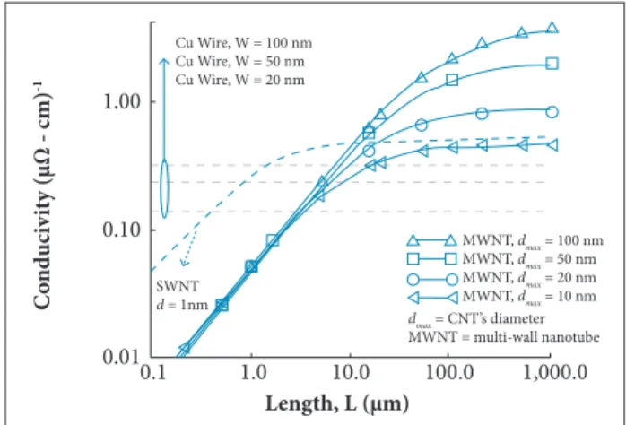
Figure 2. Conductivity for SWCNT and MWNT nanotubes as a function of length (Wong and Akinwande, 2011).
∆L Ces∆L Cq∆L
Lm∆L
Lk∆L
R∆L
Rc/2 Rc/2
C
o
nd
u
civ
it
y (μΩ - cm)
-1
Length, L (μm)
1.00
0.10
0.01
0.1 1.0 10.0 100.0 1,000.0
MWNT, dmax = 100 nm
MWNT, dmax = 50 nm
MWNT, dmax = 20 nm
MWNT, dmax = 10 nm
Cu Wire, W = 100 nm Cu Wire, W = 50 nm Cu Wire, W = 20 nm
SWNT
d = 1nm
dmax = CNT’s diameter MWNT = multi-wall nanotube
he propagation constant is in general a complex number. he real part (α) and the imaginary part (β) represent the attenuation and phase constant of the transmission line, respectively. With the given parameters of the transmission line in Fig. 1, Z0 and γ
can be determined using the classical transmission line theory.
of the signal becomes dependent upon the frequency (ω). he term Ctot is the resulting capacitance of Cq and Ces in series, according to the model presented in Fig. 1, and g is computed as g = √Ctot /Cq.
he group velocity is given by ѵg = 2√2ω/RCtot, which also depends on ω. This dependence causes undesirable signal dispersion along the metal CNT. In order to reduce the efect of attenuation and scattering of the signal, one should keep both the length and the Ces of the metallic CNT as small as possible. To decrease the inluence of ω in the ѵg, the Ces must be much smaller than the Cq (Wong and Akinwande, 2011).
In general, CNT as metallic interconnecting elements will have an advantage over the copper tracks when the CNT are in ballistic regime, as one can see in Fig. 2 (Wong and Akinwande, 2011; Javey and Kong, 2010).
he transmission line can be considered lossy when the signal frequency is much below the critical frequency and lossless when the signal frequency is much above the critical frequency. his critical frequency is usually called zero frequency (ωz) and it is deined as the ratio between R and Lk of the transmission line, i.e.ωz = R/Lk (Wong and Akinwande, 2011). For a high-quality SWCNT at room temperature and with the efective mean free path of 1 μm, ωz ≈ 318 GHz (Wong and Akinwande, 2011). In the lossless (ballistic) transmission regime, the propagation constant γ of the line is a pure imaginary number which is proportional to the frequency of the signal, i.e.γ = jβ = jgω√LkCq. In this equation, g is a parameter that quantiies the electron-electron interaction, j means that the variable is a complex number and ω is the angular frequency. When g ~1, the interaction is weak; and when g ~ 0, the interaction is strong (Wong and Akinwande, 2011). he line’s Z0, which, in this case, is given by Z0 = 1/g√LkCq, is a pure real number. It does not depend on the frequency. his means that a signal that propagates along this line does not sufer attenuation; besides, the voltage and the current of the line are in phase. he group velocity ѵg = ϑω/ϑβ is constant, i.e. all the frequency components of the signal propagate along the line with the same velocity ѵg given by ѵg = ѵF/g , where is the Fermi velocity: ѵF ≈ 108 cm.s-1 (Wong and Akinwande, 2011).
In a lossy transmission line (difusive regime), the attenuation is due to ohmic losses represented in Fig. 1 by R. he characteristic impedance is no longer a pure real number and is given by Z0 = 1/g√R/2ωCtot e-jП/4 (Wong and Akinwande, 2011). Analyzing
this expression, one can conclude that, for the metallic CNT, the voltage is delayed with respect to the current by Π/4, presenting, thus, partially capacitive behavior. In addition, the amplitude
NANODIODES WITH CNT
Figure 3. Examples of rectifying p-n junction (D’yachkov, 2006).
Figure 4. Sample image junction obtained by atomic force microscope (Yao et al., 1999): (a) CNT placed directly on 3
electrodes, (b) CNT folded that presents the effect of rectiica-tion, (c) the detail of the fold, in which, on one side of the fold, the CNT is metallic and, on the other one, it is semiconductor.
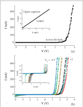
Figure 5. Current-voltage characteristic of metal-semiconductor junction in Fig. 4a.
5
(5,5)
(10,0) 7
(a) (b)
Au SiO2
I
II
7 5
(a) (b) (c)
V (V)
V (V) V (mV)
Across the kink
+2 VR = -4 V
Upper segment
110kΩ
V (V)
I (nA)
I (nA)
I (nA)
I (nA)
400
300
200
100
0
-4 -3 -2 -1 0
0 2 -4
-0.4 0.2 0.0 0.2 0.4
0 0
50
-50
5 -5
-10 10
-2
1 2
2 3
1 -1
-2
-3 0
3 4
400
300
200
100
0
(b) (a) According to Yao et al. (1999), the carbon nanotube shown in
Fig. 4a is placed directly on three electrodes. he electrodes are over a ilm of silicon dioxide (SiO2), which, in turn, is on a silicon
(Si) wafer that has the function of a gate. At room temperature, the resistance of the carbon nanotube’s upper segment between the two electrodes is 110 KΩ, shown in detail in Fig. 5a. his thread has metallic behavior and is independent of the applied gate voltage. On the other hand, the current-voltage characteristic of the carbon nanotube bend, also shown in Fig. 5a, has a highly non-linear and asymmetric behavior, resembling the current-voltage characteristics of a diode rectiier. We can observe a very high increase in the current when applying a positive voltage on the top electrode when the voltage exceeds the threshold voltage, which is about 2 V (Fig. 5a). here is a very small increase in current for the reverse bias. his junction has an extremely high impedance for the voltages around 0 V.
Figure 5b represents current-voltage characteristics of metal-semiconductor junction in Fig. 4a. he electrodes are made of gold (Au) and titanium (Ti) and have dimensions of 250 nm wide, 20 nm in thickness and less than 1 nm in height, which minimizes deformation of the CNT. he curve in Fig. 5a is obtained with the grounded gate. In Fig. 5b, the gate voltage from let to right ranges from -4 V to +2 V.
he Schottky diode is another type of diodes of particular interest for applications in the range of 30 GHz to 3 THz. he diodes that operate in this range are commonly used as detectors, mixers and frequency multipliers in the submillimeter wave region at room temperatures. he CNT diodes are characterized by their high switching speed and inherent suitability for applications at low voltages and high currents (Manohara
et al., 2005; Huang et al., 2010).
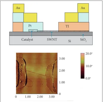
Figure 6. (a) Schottky diode’s schematic representation, (b) typical image obtained by atomic force microscope (Manohara et al., 2005).
Figure 7. Current-voltage characteristics of four Schottky diodes (Manohara et al., 2005).
Au Au
TI Pt
Catalyst SWNT Si SiO2
0 1.00 0
1.00
2.00
2.00
3.00 3.00
0.0o
10.0o
20.0o
Scholttky metal – Ti Ochmic metal – Pt
V (Volts) -14
-2x10⁻⁶
2.0x10⁻⁶
6.0x10⁻⁶
1.0x10⁻⁶
1.4x10⁻⁶
-10 -6 -2 2
I (A
m
ps)
d-1 d-2 d-3 d-4
in THz range because of small areas of the junctions, which usually have a maximum of 2 nm in diameter. his leads to low capacitances of the order of tens αF/μm. Besides, the CNT possess high electron mobility, reaching up to 200.000 cm²/V.s (Manohara et al., 2005).
Unlike planar microelectronic Schottky diode junctions, the Fermi contact level does not control the properties of devices with CNT. As a result, the best threshold voltage for optimal performance of the device can be chosen (Manohara et al., 2005; Huang et al., 2010).
Figure 6 shows the basic schematic representation of a Schottky diode, whose design employs two diferent metals at the ends of the p-type CNT. he utilized metals have diferent work functions (Φ); one of them has a lower work function than the CNT in order to have the Schottky contact; the other one has a higher work function than the CNT in order to obtain the ohmic contact (Manohara et al., 2005).
In Fig. 6a, the Schottky contact is obtained with the use of Ti, and ΦTi= 4.33 eV < ΦNTC, with ΦNTC ≈ 4.9 eV. he ohmic contact is obtained with the use of platinum (Pt) possessing, and ΦPt = 5.65 eV > ΦNTC(Manohara et al., 2005). here is a layer of SiO2 between the Si substrate and the CNT of approximately 400 nm of thickness.
Figure 7 shows the direct (DC) current-voltage characteristics of four diferent types of Schottky diode manufactured on the
same substrate and in the same batch with the zero gate voltage. All these diodes contain a single CNT with semi-conductive characteristic between the two contacts of diferent metals formed by Ti and Pt (Manohara et al., 2005). We can see in Fig. 7 that the current-voltage characteristics for the four diodes are quite diferent. hese diferences can be attributed to the characteristics of the CNT, such as, for example, its overall length and the overlap that it makes with the metallic contacts (Yang et al., 2005).
here is another type of diode, also for high frequency, which uses multiple CNT in parallel between the metal contacts of the device (Manohara et al., 2005). Each device has from 8 to 10 CNT. hese nanotubes may have either metallic or a semi-conductor behavior and this property is diicult to control. he presence of only one carbon nanotube with metal characteristics destroys the desired efect of rectiication. herefore, the CNT with metallic behavior were literally burned by a high current in the technological process that is described in Collins et al. (2001) so that all the remained tubes had semi-conductor properties. Figure 8 shows the change in current-voltage characteristic before and ater the selective burning of metallic CNT. he inset chart in this igure demonstrates the curve for the rectiier for low bias voltages.
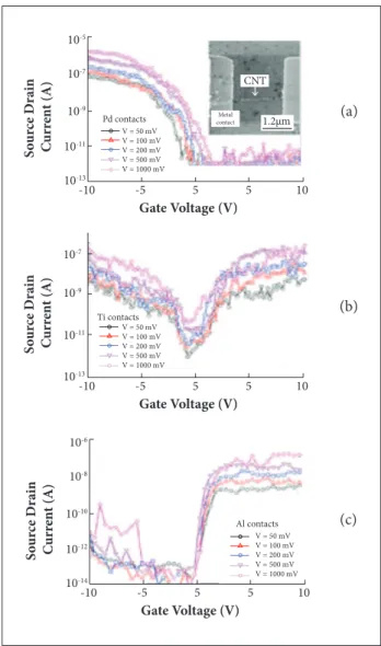
Figure 9 shows the current-voltage curves of symmetric devices, i.e. those whose metallic contacts are made of the same material. All electrical measurements were made at room temperature in the air. In Fig. 9a, palladium (Pd) was used as contact metal, resulting in a behavior of a p-type semi-conductor with on-of current ratio of 106. In Fig. 9a, it is shown in detail
Figure 9. Current-voltage curves of a symmetric Schottky diode with three different metals as contact (Avouris, 2002).
Figure 10. Image of ield-effect transistor with CNT obtained by atomic force microscope (Adel and Smith, 2007).
Drain
Nanotube
Source
-10 -5 5 5 10
10-13
10-11
10-9
10-7
10-5
Gate Voltage (V)
S o ur ce Dr ain C urr en t (A)
V = 50 mV V = 100 mV V = 200 mV V = 500 mV V = 1000 mV
Pd contacts Metal
contact 1.2μm
CNT
-10 -5 5 5 10
10-13
10-11
10-9
10-7
Gate Voltage (V)
S o ur ce Dr ain C urr en t (A)
V = 50 mV V = 100 mV V = 200 mV V = 500 mV V = 1000 mV
Ti contacts
-10 -5 5 5 10
10-14
10-12
10-10
10-8
10-6
Gate Voltage (V)
S o ur ce Dr ain C urr en t (A)
V = 50 mV V = 100 mV V = 200 mV V = 500 mV V = 1000 mV
Al contacts
(a)
(b)
(c) in an ambivalent behavior, i.e. for negative bias voltages, the
device features a semi-conductor p-type behavior and, for positive bias voltages, the same device shows a semi-conductor n-type behavior. he on-of ratio is about 104. In Fig. 9c, aluminum
(Al) was used as the metal contact, resulting in an on-of ratio of 10³ for negative gate bias voltages and an on-of ratio of 106
for positive bias voltages.
As seen in Fig. 9, the simple change of the type of material used as electrical contact modiies the current-voltage characteristic of the device, and it can present both a p-type semi-conductor behavior and an n-type semi-conductor behavior or even ambivalent characteristics.
at the top of a SiO2 ilm, which, in turn, was deposited on a Si wafer. his Si wafer operates as a third terminal, which has the function of gate. hese devices have the properties of a p-type
Figure 8. Current-voltage curve of Schottky diode with multiple CNT (Manohara et al., 2005).
NANOTRANSISTORS BASED ON CNT
In microelectronics, the basic structure of a ield-efect transistor (FET) of solid state is composed of two metal electrodes called source and drain, which are connected by a channel in a semi-conductor. here is a third electrode, called the gate, which is isolated from the channel by a thin layer of SiO2. By varying the channel width, the gate bias voltage controls the current low between the source and drain terminals.
In FET with CNT (CNFET), the Si semi-conductor channel is replaced by a SWCNT, which is inserted over the metal electrodes with high work function Φ > 5 eV. hese electrodes are typically made of Au or Pt (Avouris, 2002).
Back in 1998, there were the irst demonstrations that CNT could be used in the design of FET (Adel and Smith, 2007). An example of this transistor is shown in Fig. 10. In this picture, a carbon nanotube is positioned at the top, interconnecting thus the two electrodes of noble metals. hese electrodes are the source and drain terminals of the FET, which were fabricated
V (Volts)
V (Volts)
I (A
m
ps)
I (x 10
-4A)
Original I-V After burn-out I-V
-2 -6.0x10⁻⁶ -4.0x10⁻⁶ -2.0x10⁻⁶ 2.0x10⁻⁶ 0.0 4.0x10⁻⁶
-1 0 1 2
Figure 11. Schematic representation of ield-effect transistor with CNT with top-gate (Adel and Smith, 2007).
Figure 12. Electrical output characteristics of top-gate ield-effect transistor with CNT with source, drain and gate terminals of titanium at room temperature (Adel and Smith, 2007).
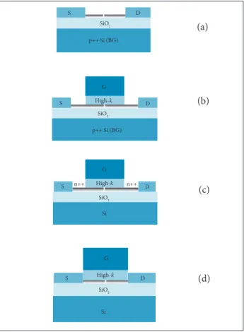
Figure 13. Geometric conigurations commonly used in ield-effect transistor with CNT (Wong and Akinwande, 2011).
Source
Gate
Nanotube
Drain
Silicon wafer
Gate oxide
Silicon dioxide
S S
Si Si
n++ n++
G G
D D
SiO2 SiO2
High-k
High-k
S S
p++ Si (BG) p++ Si (BG)
G
D D
SiO2 SiO2
High-k
(a)
(b)
(c)
(d)
Vds (V)
Vgs (V) Vgs – Vt
Vds = -0.6 V
Id
(μA)
Id
(A)
-5.0
-4.0
-3.0
-2.0
-1.0
-1.6 -1.2 -0.8 -0.4
0.0
0.0
0.0 -10-11
-1.1 V
-0.9 V
-0.7 V
-0.5 V
-0.3 V
-0.1 V
-10-10
-10-9
-10-8
-10-7
-10-6
0.8 -0.8
-1.6
FET with the ratio of on-of current of the order of 105. hey
are characterized by a high parasitic resistance of contact, which is generally around 1 MΩ, a low current between source and drain and a low transconductance of the order of 10-9 A/V.
In order to reduce the contact resistance and improve the features of the CNFET, the scheme shown in Fig. 10 can be modiied as proposed in Adel and Smith (2007). In this assembly, there is an oxidized Si wafer placed on the SiO2, in which the SWCNT is dispersed. The source and drain terminals are fabricated on top of a SWCNT semi-conductor, according to the scheme in Fig. 11. he terminals are made of Ti or cobalt (Co). he curve of Fig. 12 was obtained at room temperature, with the drain, source and gate terminals made of Ti. he thickness of the SiO2 under the gate is 15 nm. A reduction of the parasitic resistance is obtained by heat treatment between the metal and the SWCNT. As a result, the resistance was reduced from 1 MΩ to 30 KΩ, approximately. Figure 12 shows the output characteristics of this CNFET Adel and Smith (2007). he device in Fig. 11 can also be switched using a Si wafer as a back-gate.
Currently, there are several geometric conigurations that can be used in implementation of the CNFET. he most com-monly used are shown in Fig. 13 (Wong and Akinwande, 2011). In the settings of Fig. 13, all of them retain some features in common with each other, such as the use of intrinsic CNT semi-conductors with the channel function, the use of metal contacts to the terminals of the source, drain and gate. he gate can be both top-gate and back-gate and, as a common use, all conigurations make use of a dielectric or an oxide in order to isolate the gate terminal of the CNT.
The dynamics of CNFET operation is simple to understand. When a bias voltage is applied at the gate terminal of the CNFET, a perpendicular electric field appears in the channel of this device. This electric field controls the amount of charge carriers in the channel. The control can be fulfilled in two different ways: by top-gate, when the gate terminal is placed over the CNT, or by back-gate, when the gate terminal is underneath the Si wafer, which is heavily doped.
Type of contact
between metal-CNT L < lm L > lm
Ohmic Ballistic Difusive
Schottky barrier Ballistic Difusive
Table 1. The four transport regime of ield-effect transistor with CNT (Wong and Akinwande, 2011).
2-D MOSFET 1-D CNFET
Parameter Origins Parameter Origins
(i) uef Drit velocity (i) φs Gate coupling (ii) I/L Drit velocity (ii)Eg Band structure (iii) Cox/W Charge sheet (iii) Rq
Quantum transport
(iv) V2
Drit velocity and charge
sheet
(iv) kgT Fermi-Dirac
distribution
Table 2. Difference between 2-D MOSFET and 1-D CNFET (Wong and Akinwande, 2011).
ION≈ueff CoxW (VG–VT) 2 ION≈ kBT ln 1 + e
2eφs- Eg
2L eRq
2kBT now, through an electrostatic doping in a region of the CNT
near of the drain and source terminals in order to decrease the contact resistance between these terminals. his doping is done by electrostatic application of vertical electric ield that induces electrons or holes near the region of the drain source terminals. Regardless of the type of control used, whether by a top-gate or a back-gate, there is an electric ield due to the applied bias between drain and source. his electric ield is responsible for the displacement of charge carriers between the drain and source terminals, whose intensity is controlled by the gate terminal.
Four basic geometry settings of CNFET are shown in Fig. 13. Figure 13a depicts the scheme of the device of Fig. 10, in which the Si substrate is heavily doped and plays the role of back-gate. he diference between Fig. 13b and Fig. 13a is that there is an additional electrode G which plays the role of top-gate. he top-gate is separated from the CNT by a high-k dielectric (the high-k dielectric has the dielectric constant k several times much greater than that of SiO2). Therefore, in this geometry, one can control the current low between source and drain terminals, both through the top-gate and by the back-gate. Figure 13c uses the chemical doping in the regions close to the source and drain terminals, and Fig. 13d depicts the geometry of a top-gate with a self-aligned CNFET, which implies a perfect alignment, i.e. no space between the gate, source and drain metal contacts. Controlled devices through the top-gate are preferred when a greater control of the channel is desired, as well as the top-gate allows the control of individual top-gates on a device with multiple transistors. Notice that the charge carriers in CNFET can be both electrons and holes (Wong and Akinwande, 2011). In Table 1, the four charge transport schemes for CNFET are represented. hese schemes are independent on the geometric setting. hey are deined by the length, the mean free path of the CNT and the type of contact between the terminals, i.e. the ohmic or Schottky barrier. In Table 1, L is the length and Lm is the mean free path of the CNT.
In the projects of CNFET devices, one needs to optimize the current between source and drain terminals. In this sense,
projects with transparent contacts (i.e. ohmic contacts) and ballistic transport ofer the best performance.
DIFFERENCES BETWEEN 2-D METAL-OXIDE-SEMICONDUCTOR FIELD-EFFECT TRANSISTOR AND 1-D CNFET
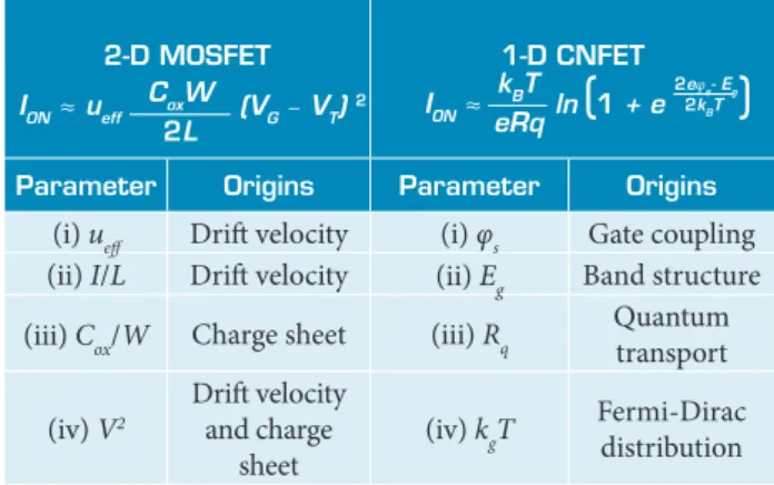
In Table 2, a comparison between the 2-D metal-oxide-semiconductor field-effect transistor (MOSFET) and 1-D CNFET is given. Due to the 1-D nature of CNT, in the linear region, the electrons can move only in one direction, i.e. either forward or backward and the charge transport can be ballistic. As for the MOSFET, the electrons can move in the plane and the electrons transport is difusive. In the active regions of the MOSFET, the current of saturation is due to the pinch-of that occurs in the channel and, as a consequence, the drit rate no longer depends on the drain voltage (Martel et al., 2001). As for CNFET, the current of saturation occurs due to disappearance of the charge carriers from the drain terminal. his implies that the current does not depend on the drain voltage, unlike of what occurs with the MOSFET (Wong and Akinwande, 2011). Table 2 shows explicitly that the device current in the on state (ION) for the MOSFET is controlled mainly by the drit velocity (uef), which depends on the properties of the material. Whereas for CNFET this current mainly depends on the physical properties of states of the electrons in the solid, such as the band-gap structure (Eg), the Boltzmann constant (ks) depends on the temperature (T) and the quantum resistance (Rq) (Wong and Akinwande, 2011). he parameter uef is the drit velocity, which is an indicative of the average scattering that the loads sufer in the solid; L and W are the length and width of the channel, respectively; Cox is the capacitance of the insulating placed between the top-gate and the channel; φs is
the electrostatic surface potential; VG is the gate voltage and VT is the threshold voltage. he other parameters of Table 2 have already been described in the text.
A more detail information about the topics of this paper can be found in references below.
CNT DEVICE SIMULATIONS
In the nanoscale simulations, one needs to consider the efects of a single atom on the characteristics of the device. In the atomic scale, the efects of the individual vacancies and impurities start to have a real inluence in the performance of the device.
There are two main steps in the nanoelectronic studies. he irst one is a solution of the electronic structure problem that deals with the behavior of electrons’ band energy inside of the material as well the DOS in such energy levels. In practice, this study gives us the information about the band gap and the energy levels where the device will work properly. Two categories of methods are used in practice: ab initio approaches to solve the Schrödinger equation based on irst principles. An example of such methods is density-functional theory (DFT). he second category is semi-empirical methods where the electronic structure is calculated by using adjustable parameters obtained, for example, from experiments.
he second step is the study of electronic transport, i.e. the behavior of the electronic current inside the material. he problem here is usually to obtain the I-V (current-voltage characteristic) curves. In this step, it is necessary to consider the electrons as wave functions instead of particles. hat is, it is important to take into account the quantum efects that appear in the atomic scales. At these scales, the channel of the device (the active region of interest) is frequently shorter than the mean-free path of the material. hus, one has to take into account the potential proile of the central region; has to consider quantum mechanical equations and approximation, such as Schrödinger equation; needs to apply, in the right
way, the boundary conditions; and has to consider the non-equilibrium situation because the transmission property of the electron is itself bias dependent — that is the problem is non-linear and, for each value of applied voltage, one has a diferent transmission curve. A combination of the Landauer approach with the non-equilibrium Green function (NEGF) method is now widely used in the analysis and design of nanoscale devices. Quantum transport in nanotubes and other nanoelectronic devices is described in more details in (Wong and Akinwande, 2011; Javey and Kong, 2010; Stokbro et al., 2010; Blom and Stokbro, 2011; Datta, 2005; Nazarov and Blanter, 2009).
CONCLUSION
Some special electrical, optical and magnetic properties, the mechanical strength and chemical stability make the CNT one of the promising nanomaterials to be used in nanoelectronics.
Based on the available literature, this study shows that the devices with CNT are very promising for replacing microelectronic devices that employ Si, germanium (Ge) or GaAsas semi-conductor elements. he use of CNT as a metal to interconnect elements in order to replace the copper tracks is advantageous when the mean free path is smaller than the link track.
The use of CNT in the projects of diodes and FETs allows one to increase the frequency range of these devices, sometimes even to THz. Possible applications of such devices are detectors, mixers, frequency multipliers, among others. However, there are still some challenges to be overcome in order to raise the manufacturing process of these CNT devices to a commercial scale, such as control of the physical and electronic properties in the CNT growth process. he production of CNFET is still complicated, expensive and requires a lot of time.
REFERENCES
Adel, S. and Smith, K.C., 2007, “Microeletrônica”, Fifth Ed., Prentice Hall, São Paulo, Brazil.
Avouris, P., 2002, “Molecular Electronics with Carbon Nanotubes”, Accounts of Chemical Research, Vol. 35, No. 12, pp. 1026-1034. doi: 10.1021/ar010152e
Blom, A. and Stokbro, K., 2011, “Towards Realistic Atomic-Scale Modeling of Nanosacale Devices”, IEEE Conference on Nanotechnology, pp. 1487-1492. doi: 10.1109/NANO.2011.6144584
D’yachkov, P.N., 2006, “Carbon Nanotubes: Structure, Properties and Applications”, BINOM, Moscow, Russia.
Datta, S., 2005, “Quantum transport. Atom to transistor”, Cambridge University Press, Cambridge, UK. 404p.
Dragoman, M. and Dragoman, D., 2006, “Nanoelectronics: Principles and Devices”, Artech House, Boston, USA/London, UK. 426p.
Huang, L., Chor, E.F., Wu, Y. and Guo, Z., 2010, “Fabrication of Single-Walled Carbon Nanotube Schottky Diode with Gold Contacts Modiied by Asymmetric Thiolate Molecules”, Carbon, Vol. 48, No. 4, pp. 1298-1304. doi:10.1016/j.carbon.2009.12.003
Iijima, S., 1991, “Helical Microtubules of Graphitic Carbon”, Nature, Vol. 354, pp. 56-58,. doi: 10.1038/354056a0
Javey, A. and Kong, J., 2010, “Carbon Nanotube Electronics”, Springer, New York, USA.
John, D.L., Castro, L.C. and Pulfrey, D.L., 2004, “Quantum Capacitance in Nanoscale Device Modeling”, Journal of Applied Physics, Vol. 96, No. 9, pp. 5180-5184.
Manohara, H.M., Wong, E.W., Schlecht, E., Hunt, B.D. and Siegel, P.H., 2005, “Carbon Nanotube Schottky Diodes Using Ti-Schottky and Pt-Ohmic Contacts for High Frequency Applications”, Nano Letters, Vol. 5, No. 7, pp. 1469-1474.
Martel, R., Derycke, V., Lavoie, C., Appenzeller, J.and Chan, K.K., 2001, “Ambipolar Electrical Transport in Semiconducting Single-Wall Carbon Nanotubes”, Physical Review Letters, Vol. 87, No. 25, pp. 256805. doi: 10.1103/PhysRevLett.87.256805
Nazarov, Y. and Blanter, Y., 2009, “Quantum Transport. Introduction to Nanoscience”, Cambridge University Press, Cambridge, UK.
Sadiku, M.N.O., 2004, “Elementos de Eletromagnetismo”, Third Ed., Bookman, Porto Alegre, Brazil.
Stokbro, K., Peterson, D., Smidstrup, S., Blom, A., Ipsen, M. and Kaasbjerg, K., 2010, “Semiempirical Model for Nanoscale Device Simulations”, Physical Review B, Vol. 82, No. 7, 075420. doi: 10.1103/PhysRevB.82.075420
Wong, H.S.P. and Akinwande, D., 2011, “Carbon Nanotube and Graphene Device Physics”, Cambrigde University Press, Cambrigde, UK. 262p.
Yang, M.H., Teo, K.B.K., Milne, W.I. and Hasko, D.G., 2005, “Carbon Nanotube Schottky Diode and Directionally Dependent Field-Effect Transistor Using Asymmetrical Contacts”, Applied Physics Letters, Vol. 87, 253116.