Brazilian Journal of Physics, vol. 34, no. 2B, June, 2004 581
Epitaxial Hybrid Ferromagnet-Semiconductor Structures:
Growth, Structural and Magnetic Properties
L. D¨aweritz
Paul Drude Institute for Solid State Electronics, Hausvogteiplatz 5-7, D-10117 Berlin, Germany
Received on 9 March, 2003
Ferromagnet-semiconductor heterostructures are promising materials for the integration of magnetic or spin related functions into semiconductor materials and devices. Fe-on-GaAs and MnAs-on-GaAs are canditates for potential room temperature applications. We review our recent results on growth, structural and magnetic properties of these materials, and their use as spin injectors. The most critical issue of Fe/GaAs heterostructures is the delicate interface formation during epitaxy and its possible modification during subsequent processing. The properties of the MnAs/GaAs heterostructures are intimately related to the phase transition between ferro-magnetic and paraferro-magnetic phases.
1
Introduction
The introduction of magnetic or spin related functions into semiconductor materials and devices became a subject of intense research over the past few years [1-3]. In particular, the desire to use not only the charge but also the spin of elec-trons for the development of novel devices motivated work about monolithic integration of ferromagnetic and semi-conductor materials using ultra-high vacuum growth tech-niques. A key of success is the epitaxial growth of het-erostructures with well-ordered heterointerfaces which al-low spin injection from the ferromagnetic layer into the semiconductor. Heterostructures of high structural quality can be realized in particular for the case of low lattice mis-match between similar materials. However, layer structures like Ga1−xMnxAs on GaAs exhibit a Curie temperature
be-ing far below room temperature [4]. Two promisbe-ing mate-rial systems for spin injection at room temperature are Fe-on-GaAs and MnAs-Fe-on-GaAs. Epitaxial growth of such dis-similar materials encounters specific problems, like the ther-modynamic stability of the interface, large anisiotropic mis-fit, and phase transitions. In this article, we review our re-cent results on low-temperature growth of Fe-on-GaAs and MnAs-on-GaAs heterostructures by molecular beam epitaxy (MBE), their structural and magnetic properties, as well as the successful use of the ferromagnetic layers as spin injec-tors.
2
Results and Discussion
A. Fe-on-GaAs
Fe-on-GaAs is the most widely investigated epitaxial ferromagnetic metal-semiconductor hybrid system [5-7]. The stable bcc Fe phase, with its bulk lattice constant be-ing nearly half that of GaAs (2aF e/aGaAs= 1.012), grows in
(001) orientation on GaAs(001) with Fe[100]||GaAs[100]. In the majority of investigations Fe has been deposited at elevated temperatures (150–180◦C). Under such conditions interfacial reactions occur with detrimental consequences for the ferromagnetic properties of the first few nanometers. However, no indications for the formation of FexGayAsz
alloys were found by x-ray diffraction in 20-nm-thick films at a growth temperature of 50◦C in contrast to the case of 175◦C growth temperature [8]. Such films grow by quasi-twodimensional nucleation and coalescence of nanometer-scale islands.
Recently, the ferromagnetic properties of ultrathin lay-ers grown at 50◦C were studied [9]. For layer thicknesses <10monolayers (ML) the in-plane magnetization of such films exhibits a strong uniaxial anisotropy with the easy and hard axis of magnetization parallel to GaAs[110] and GaAs [¯110], respectively. With decreasing film thickness a strong reduction of the Curie temperature is observed, which could originate from the decreasing number of neighbour-ing atoms. Ferromagnetic behavior at room temperatur is observed in films as thin as 3.5 ML. The saturation magne-tization of films withdF e ≥4 ML forT →0 K is found to
be close to the value of bulk bcc Fe(100) which amounts to 1740 emu/cm3
.
582 L. D¨aweritz
independently measured out-of-plane magnetization of the Fe layer. This demonstrates successful spin injection with an efficiency of≈5 % [10,11]. The observed spin injec-tion from a ferromagnetic metal into a semiconductor can be explaind by tunneling through a Schottky barrier at the interface [12].
B. MnAs-on-GaAs
Bulk MnAs is ferromagnetic with a hexagonal NiAs structure below ≈40◦C, where it experiences a first-order phase transition to a paramagnetic β-MnAs phase with an orthorhombic structure. A further transition occurs at ≈125◦C to paramagneticγ-MnAs, which has again a NiAs structure [13].
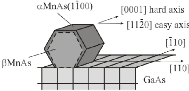
Ferromagnetic MnAs can be grown epitaxially on GaAs(001), although the lattice mismatch is very large and anisotropic, i.e., 7.5% along the GaAs[110] direction and about 30% along the GaAs[¯110] direction [14,15] (see Fig. 1). Two fundamental issues for understanding this unex-pected result of real heteroepitaxy have been identified: (i) an interesting anisotropic lattice mismatch accommodation mechanism [16] and (ii) the strain-mediated coexistence of α- andβ-MnAs below the bulk phase transformation tem-perature [17].
Figure 1. Scheme of the epitaxy of MnAs on GaAs(001) and ori-entation of the hard and easy axis of magnetization.
By controlling the stoichiometry of the GaAs template and the MnAs growth conditions, several epitaxial orienta-tions can be realized [14,15]. Our films were grown at con-ditions (substrate temperature 250◦C, As4:Mn beam equiv-alent pressure ratio of 90, growth rate 20 nm h−1
) lead-ing to the unique A-orientation (Fig. 1). The MnAs(1¯100)
plane is parallel to GaAs(001) and the MnAs[0001] direc-tion, which is also the hard axis of magnetizadirec-tion, is parallel to GaAs[¯110]. The easy axis of magnetization lies also in-plane along the MnAs[11¯20] direction which is parallel to GaAs[110].
As observed in situ by reflection high-energy electron diffraction (RHEED) and confirmed by scanning tunneling microscopy, in early growth stages three-dimensional is-lands exist before after deposition of about 5 ML due to coalescence a smooth film develops [18]. Further growth on such a surface proceeds layer-by-layer as evidenced by RHEED intensity oscillations [19]. High-resolution transmission electron microscopy studies show that the MnAs/GaAs interface is smooth and chemically sharp [16].
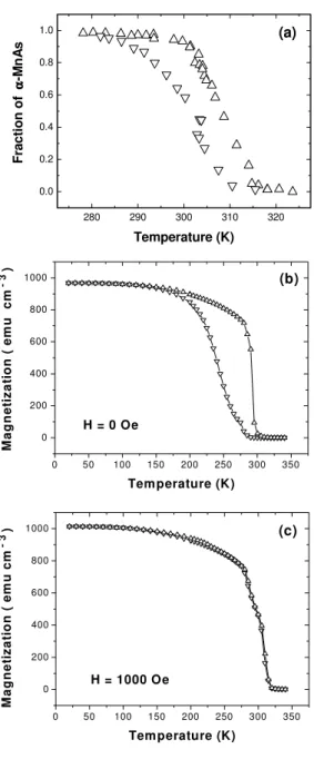
In thicker films, in addition to theα-phase of MnAs the β-phase is detected by x-ray diffraction. In Fig. 1 the unit cell of the orthorhombicβ-phase is shown using a dashed line. At the β → αphase transition during cooling from growth to room temperature, the plane corresponding to (0001) of the α-phase expands discontinously by ≈1.2%, whereas the change along [0001] is comparatively small [20]. The epitaxial constraints of the film lead to an equi-librium coexistence between α- andβ-MnAs over a wide temperature interval [17]. The phase composition of the films is obtained from ω-2θ x-ray diffraction scans which show two separate [1¯100] and (020) peaks for theα- andβ -phase, respectively. The ratio of their integrated intensities gives the fraction ofα-MnAs. Fig. 2(a) presents data for heating and cooling of a 180-nm-thick film. The fraction of α-MnAs almost linearly increases upon cooling in a temper-ature interval of more than 20 K. The phase coexistence is accompanied by a temperature hysteresis.
As a result of the epitaxial strain induced at theβ →α phase transition, a striped phase separation occurs [17,21]. A self-organized pattern with a periodic array of ridges and grooves is observed at room temperature (Fig. 3(a)). The groove direction is along MnAs[0001]. The ridges consist ofα-MnAs and the grooves ofβ-MnAs.
To give direct evidence for the assignment of the ridges to the ferromagneticα-phase, we employed magnetic force microscopy (MFM) [22]. By varying the working distance of the cantilever, images with topographical and magnetic contrast of the same area are obtained. Magnetic contrast as meander-like structure is found only in the area of the ridges. In neighbouring domains, the magnetic moments are oriented opposite to each other, i.e., along [11¯20] and [¯1¯120], respectively. Since [0001] is the hard axis of mag-netization and the out-of-plane [1¯100] direction is a medium axis of magnetization, the rotation of the magnetic moment occurs via an out-of-plane rotation, giving rise to the ob-served magnetic contrast [23]. This meander-like contrast is due to domain walls of the Bloch-type.
The dynamics of the phase transition has been studied by employing temperature-dependent scanning probe mi-croscopy to image the topography [24]. The development of a rippled surface morphology with a periodic arrangement of ridges and grooves is observed in the temperaure range from about 40◦C to 12◦C. While the ridges, which appear just below the Curie temperature of MnAs, are initially in an irregular arrangement, an ordereing process takes place at lower temperature. The width of the ridges increases upon cooling, until finally the grooves are completely closed.
Brazilian Journal of Physics, vol. 34, no. 2B, June, 2004 583
is an abrupt disappearance of magnetization due to split-ting into domains. It is not discontinuous as expected for an ideal first-order phase transition from the ferromagnetic to the paramagnetic state [25]. In agreement with the phase composition (cf. Fig. 2(a)), the spontaneous magnetization becomes zero at≈315 K. Thus, the heating branches of the magnetization curve and of the phase composition curve are strongly correlated and the apparent deviation from a first-order magnetic transition is due to the strain-mediated phase coexistence ofα- andβ-MnAs.
280 290 300 310 320 0.0
0.2 0.4 0.6 0.8
1.0 (a)
Fra
c
ti
on
o
f
α
-M
n
A
s
Temperature (K)
0 50 100 150 200 250 300 350 0
200 400 600 800 1000
H = 0 Oe
(b)
Temperature (K)
M
a
g
n
e
ti
z
a
ti
o
n
( e
m
u
c
m
- 3
)
0 50 100 150 200 250 300 350 0
200 400 600 800 1000
H = 1000 Oe
(c)
Temperature (K)
M
a
gne
ti
z
a
ti
on
(
e
m
u
c
m
3 )
Figure 2.(a) Fractions of α-MnAs obtained on heating and cool-ing of a 180-nm-thick MnAs film. Temperature dependence of the magnetization measured without external magnetic field (b) and with applying a field of 1000 Oe (c). Heating and cooling branches are indicated by triangles up and down, respectively.
(a)
M n A s [00 0 1]
(b)
∆z = 4 n m
Figure 3. MFM images of a 180-nm-thick MnAs film. Both images represent the same scanning area (6µm×7µm) with topography-induced contrast (a) and contrast topography-induced by magnetic signal (b).
Upon cooling, the magnetization is not re-established at 280 K (Fig. 2(b)) although the film consists already com-pletely ofα-MnAs (Fig. 2(a)). The cooling branch matches the heating branch not before a temperature as low as≈150 K is reached.
Insight into the large asymmetry of this ferromagnetic-paramagnetic phase transition provides a recent study of the MnAs films with x-ray magnetic circular dichroism pho-toemission electron microscopy (XMCDPEEM) [26]. As schematically shown in Fig. 4(a), the XMCDPEEM im-age of a film in theα → β transition stage upon heating from below 273 K reveals ferromagnetic domains, which are strongly elongated in [0001] direction. In neighbour-ing domains the magnetic moments are oriented opposite to each other. The paramagnetic stripes perpendicular to the easy axis break the domains up into narrow stripes, which are still well correlated. In a MnAs film cooled from the completely paramagnetic state to room temperature there is yet mainly ferromagnetic coupling between the neighbour-ing ferromagnetic stripes. But many oppositely magnetized regions occur, too, as sketched in Fig. 4(b).
(a) (b)
a
b
a
M
[0001]
[1
120]
Figure 4. Schematic representation of the array of magnetic do-mains in the coexistence range of theα- andβ-phase of a MnAs film upon heating from below 273 K (a) and upon cooling from the completely paramagnetic state (b).
584 L. D¨aweritz
correlates with that of the heating branch of the phase com-position curve, suggesting that the hysteresis of the compo-sition curve can be lifted by applying a magnetic field.
50-nm-thick MnAs layers were used for spin injection at 80 K [11]. The electrical spin injection from MnAs into GaAs was again studied by means of the circular polariza-tion of electroluminescent light from an an invertedn−i−p (Ga,In)As LED in the same configuration as described for the Fe-on-GaAs system. A spin injection efficiency of about 6% was obtained.
3
Conclusion
Ferromagnetic Fe and MnAs layers with high-quality inter-faces can be grown by MBE on GaAs(001). Utilizing the optical signal from a (Ga,In)As LED spin injection from both Fe and MnAs into GaAs with an efficiency of about 5% was abserved at room temperature and at 80 K, respectively. Most of the properties of the Fe-on-GaAs heterostructures can directly be correlated with the intricate ferromagnet-semiconductor interface formation during growth and modi-fication during subsequent processing. MnAs-on-GaAs het-erostructures, on the other hand, have a high thermal sta-bility but show a complex structural and magnetic behavior. In particular, a phase separation process during cooling af-ter growth leads to an inaf-teresting self-organized pataf-tern with alternating stripes of ferromagneticα-MnAs and paramag-neticβ-MnAs.
Acknowledgement
The author wishes to thank K. H. Ploog for continuous support and the colleagues C. Herrmann, T. Hesjedal, B. Jenichen, M. K¨astner (now at European Patent Office, H V Rijswijk, The Netherlands), and T. Plake for active contri-butions to this work. Part of this work was sponsored by the Bundesministerium f¨ur Bildung and Forschung.
References
[1] G. A. Prinz, Science250, 1092 (1990).
[2] G. A. Prinz, Phys. Today48, 58 (1995).
[3] M. Tanaka, Semicon. Sci. Technol.17, 327 (2002).
[4] Y. Ohno, D. K. Young, B. Beschoten, F. Matsukara, H. Ohno, and D. D. Awschalom, Nature (London)402, 790 (1999).
[5] J. J. Krebs, T. Jonker, and G. A. Prinz, J. Appl. Phys.61, 2596 (1987).
[6] E. M. Kneedler, B. T. Jonker, P. M. Thibado, R. J. Wagner, B. V. Shanabrook, and L. J. Whitman, Phys. Rev. B56, 8163 (1997).
[7] Y. B. Xu, E. T. M. Kernohan, D. J. Freeland, A. Ercole, M. Tselepi, and J. A. C. Bland, Phys. Rev. B58, 890 (1998).
[8] H.-P. Sch¨onherr, R. N¨otzel, W. Q. Ma, and K. H. Ploog, J. Appl. Phys.89, 169 (2001).
[9] K. H. Ploog, J. Herfort, H.-P. Sch¨onherr, M. Moreno, S. Dhar, J. Crystal Growth251, 292 (2003).
[10] H. J. Zhu, M. Ramsteiner, H. Kostial, M. Wassermeier, H.-P. Sch¨onherr, and K. H. Ploog, Phys. Rev. Lett.87, 016601 (2001).
[11] M. Ramsteiner, H. Y. Hao, A. Kawaharazuka, H. J. Zhu, M. K¨astner, R. Hey, L. D¨aweritz, H. T. Grahn, and K. H. Ploog, Phys. Rev. B66, 081304 (2002).
[12] E. I. Rashba, Phys. Rev. B62, R16267 (2000).
[13] H. Okamoto, Bull. Alloy Phase Diagrams10, 549 (1989).
[14] M. Tanaka, J. P. Harbison, M. C. Park, T. Shin, and G. M. Rothberg, J. Appl. Phys.76, 6278 (1994).
[15] F. Schippan, A. Trampert, L. D¨aweritz, and K. H. Ploog, J. Vac. Sci. Technol. B17, 1716 (1999).
[16] A. Trampert, F. Schippan, L. D¨aweritz, and K. H. Ploog, Appl. Phys. Lett.78, 2461 (2001).
[17] V. M. Kaganer, B. Jenichen, F. Schippan, W. Braun, L. D¨aweritz, and K. H. Ploog, Phys. Rev. B66, 045305 (2002).
[18] M. K¨astner, F. Schippan, P. Sch¨utzend¨ube, L. D¨aweritz, and K. H. Ploog, J. Vac. Sci. Technol. B18, 2052 (2000).
[19] F. Schippan, M. K¨astner, L. D¨aweritz, and K. H. Ploog, Appl. Phys. Lett.76, 834 (2000).
[20] B. T. M. Willis and H. P. Rooksby, Proc. Phys. Soc. (London) B67, 290 (1954).
[21] M. K¨astner, C. Herrmann, L. D¨aweritz, and K. H. Ploog, J. Appl. Phys.92, 5711 (2002).
[22] L. D¨aweritz, M. K¨astner, T. Hesjedal, T. Plake, B. Jenichen, and K. H. Ploog, J. Crystal Growth251, 297 (2003).
[23] F. Schippan, G. Behme, L. D¨aweritz, K. H. Ploog, B. Dennis, K.-U. Neumann, and K. R. A. Ziebeck, J. Appl. Phys. 88, 2766 (2000).
[24] T. Plake, M. Ramsteiner, V. M. Kaganer, B. Jenichen, M. K¨astner, L. D¨aweritz, and K. H. Ploog, Appl. Phys. Lett.80, 2523 (2002).
[25] C. P. Bean and D. S. Rodbell, Phys. Rev.126, 104 (1962).