252 Brazilian Journal of Physics, vol. 36, no. 2A, June, 2006
Variable Range Hopping Conduction in Low-Temperature Molecular
Beam Epitaxy GaAs
R. M. Rubinger*, H. A. Albuquerque†, R. L. da Silva†, A. G. de Oliveira†, G. M. Ribeiro†, W. N. Rodrigues†, C. P. L Rubinger*, and M. V. B. Moreira†
∗
Departamento de F´ısica e Qu´ımica, Instituto de Ciˆencias,
Universidade Federal de Itajub´a, Caixa Postal 50, 37500-903, Itajub´a, Brazil and
†Departamento de F´ısica, Instituto de Ciˆencias Exatas,
Universidade Federal de Minas Gerais, Caixa Postal 702, 30123-970, Belo Horizonte, Brazil
Received on 4 April, 2005
Electric transport properties measured by Van der Pauw resistivity experiments of Low-Temperature Molec-ular Beam Epitaxy (LT-MBE) GaAs samples are used to identify a method to improve the resistivity of GaAs material. We present results on five samples grown at 265, 310, 315, 325, and 345oC. The electric measure-ments were carried out at temperatures ranging from 130 to 300 K. In this temperature range the dominant transport process is identified as variable range hopping. The hopping parameter plotted against the growth temperature is shown to present a maximum. The mechanisms responsible for this behavior are discussed in relation to the compensation ratio.
Keywords: GaAs; Variable range hopping; Resistivity measurements
I. INTRODUCTION
The search of GaAs layers grown by MBE with good qual-ity semi-insulating (SI) properties has been pursued for at least two decades [1] and it can be improved by the control of in-trinsic defect density through the growth temperature.
The SI characteristic is related to the presence of intrinsic deep level defects [2]. Although deep levels leads to recom-bination, in high enough density it also transport carriers by hopping. This is an undesirable characteristic. In the present work we varied the growth temperature in an attempt to max-imize the resistivity.
Albeit its technological implications, from the academic point of view, the study of hopping conduction of deep level defects on GaAs offers a fruitful platform for the study of hop-ping conduction at temperatures as high as the room temper-ature [3,4]. Previous reports on the litertemper-ature have identified hopping conduction among arsenic antisite defects (AsGa)in
GaAs [3,4]. We present here our results for resistivity mea-surements in five LT-MBE GaAs samples. The contributions of the present work concern only to the Variable Range Hop-ping (VRH).
Temperature dependent Van der Pauw resistivity measure-ments for the five samples show VRH signature associated with the law ρ =ρ0.exp(T0/T)1/4 over a wide temperature range. The parameterT01/4is an indirect measurement of the density of centers participating in hopping conduction and is a signature of the VRH. It is observed that for increasing growth temperature (TG)the hopping parameter presents a maximum
at 315oC. Such feature is associated with a low compensation
ratio. Another important issue concerns the trapping charac-teristics of deep level defects in the temperature range consid-ered in this work. This makes negligible any contribution of shallow extrinsic impurities and of free carriers as indicated by pure VRH.
II. EXPERIMENTAL DETAILS AND RESULTS
In the present work we report on VRH in LT-MBE GaAs samples grown at 265, 310, 315, 325, and 345oC. The LT-GaAs layers were grown on (100) semi-insulating LEC LT-GaAs substrates, in a RIBER 2300 MBE system. After the standard desorption procedures a buffer layer 0.21µm thick was grown at 610oC under an As overpressure of 3.2x10⁻⁵Torr and 0.81 monolayer/s. After that the substrate temperature was ramped down to the final desired temperature at 10 oC/min while growing. After reaching the set temperature GaAs epilayers were grown having around 2.4µm thick.
Microprobe analyses were carried out in order to determine the excess arsenic of the samples by comparing them with a standard GaAs wafer. The measurements were done in a JEOL JXA-8900RL in the wavelength dispersive mode con-sidering 10 different regions per sample, 1µm diameter spots, an acceleration voltage of 25 kV, and a counting time of 10 s. The excess arsenic as a function of the growth temperature are listed in Table I.
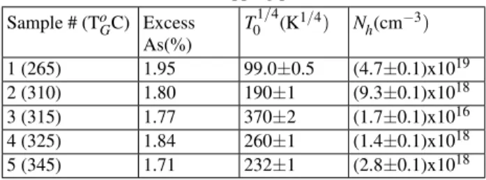
TABLE I: Hopping parameters
Sample # (To
GC) Excess As(%)
T01/4(K1/4) Nh(cm−3)
1 (265) 1.95 99.0±0.5 (4.7±0.1)x1019 2 (310) 1.80 190±1 (9.3±0.1)x1018
3 (315) 1.77 370±2 (1.7±0.1)x1016 4 (325) 1.84 260±1 (1.4±0.1)x1018 5 (345) 1.71 232±1 (2.8±0.1)x1018
R. M. Rubinger et al. 253
the applied bias was previously identified from I(V) conduc-tivity measurements, which were carried out from negative to positive bias.
For each growth temperature, we have prepared at least seven samples from different parts of the wafer and the results did not vary significantly in a same wafer. For the resistivity measurements, we have used a Keithley electrometer model 6517 and a current/voltage source Keithley model 237. Both instruments were used with triaxial cables in guarded-mode measurements. The electric transport measurements were car-ried out at temperatures ranging from 130 to 300 K.
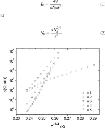
Resistivity measurements in a logarithmic scale as a func-tion of T−1/4are shown in Fig. 1. Standard VRH (vari-able range hopping) corresponds to the range of linear depen-dence of measurements in this diagram [5]. The values of T01/4obtained by fitting this linear region are listed in Table I.
III. DISCUSSION
According to Mansfield [6] the active center density carry-ing Variable Range Hoppcarry-ing (VRH) – denotedNh – can be
obtained fromT0(in K) combining the following expressions:
T0= 49 kN0a3
, (1)
and
N0=
κNh2/3
e2 (2)
FIG. 1: VRH characteristic resistivity plot versusT−1/4.
In Eq. (1) factor 49 is the percolation parameter, k is the Boltzmann’s constant andais the wave function localization radius of the hopping active center. The value ofa, which es-timated the localization radius of the defect, was eses-timated to be 4 ˚A from X-ray diffraction experiments by Shimoghishi et.
al. [7]. Finally, Eq. (2) relatesN0toNh, where the dielectric
constantκis assumed to be 12.9∈0for GaAs [3] (where∈0is the vacuum dielectric constant) andeis the electron charge. N0is directly related to the density of states associated with the AsGa[6]. It should be noted thatNh <ND, i.e.,Nhis
al-ways smaller thanND, which is the AsGadonor density or any
other defect responsible for the VRH effect. SinceNhvalues
were obtained fromT01/4which is obtained by linear fittings of Fig. 1 its value holds for the temperature range considered in the fittings.
The hopping conduction involves only the energy levels within a narrow range near the Fermi level, and this range shrinks as the temperature is reduced [8]. By decreasing the temperature, the active defect density for hopping conduction also decreases. The shrinking of the narrow energy range is the key mechanism behind theexp(T0/T)1/4law for VRH.
In Table I, besides the excess arsenic and theT01/4values, we listed theNh values calculated using Eq.(1) and Eq.(2).
The ionization energy of the defect center was 0.65 eV [4]. In this work we improved substrate characteristics by ad-justing the growth temperature and reducingNh. Since
mi-croprobe measurements indicates an almost constant excess arsenic which implies in low AsGadensity changes. The
re-duction inNhcan be associated with the compensation factor [6].
Based on the results presented in Table 1, the main out-comes can be summarized as follows. The order of magnitude ofNh, derived from resistivity measurements and Eq.(1) and
Eq.(2), decreases from 1019cm−3for sample #1 to 1018cm−3 for sample #2 and further to a minimum at 1016cm−3for sam-ple #3. The samsam-ple #3 presents the lowestNhvalue and for
further increasingTG,Nhincreases back to 1018cm−3. A
min-imum inNhmust be related to a low compensation levels and
not to a real decrease in the AsGadensity.
The microprobe analysis indicates excess arsenic between 1.71% and 1.95%. In first approximation it can be considered constant, when compared with the huge significant change in the hopping active defects densityNh(namely, three orders of
magnitude). The AsGa defect density (ND)of sample #3 is
expected to be around 1019cm−3, [9] only one order of mag-nitude lower than sample #2 and the same order of the other samples. Another mechanism must be therefore considered in order to understand the reduction of the density of active cen-ters supporting VRH. TheAs+Ga density depends directly on the acceptor densityNA. In LT-MBE GaAs the gallium
vacan-ciesVGaplay the major role as acceptors [10]. This defect is
known as a deep triple acceptor [7]. Regarding theVGa
con-centrations, Gebauer et al. [10] found densities of 1018cm−3 and 1017cm−3forT
Gof 200oC and 300oC, respectively.
LT-254 Brazilian Journal of Physics, vol. 36, no. 2A, June, 2006
MBE samples grown at 315oC are highly resistive, presenting a higher hopping parameterT01/4.
IV. SUMMARY
We carried out high-precision van der Pauw resistivity mea-surements on five GaAs samples grown by low temperature molecular beam epitaxy (LT-MBE) at 265, 310, 315, 325, and 345 oC. Our results show that the samples grown at 265oC
present resistivity and hopping parameters similar to previous ones [3]. The other samples present higher hopping parame-ter with an extremum for the sample grown at 315oC. This
result could be understood in the framework of the Variable Range Hopping mechanism, and indicates that very high insu-lating materials can be obtained by LT-MBE, when the proper growth temperature window is chosen.
Acknowledgements
The compositional measurements were done in the Labo-rat´orio de Microscopia Eletrˆonica e Microan´alise – LMA – financed by FAPEMIG under contract CEX 1074/95.
We would like to thank K. Krambrock for the elucidative discussion. The authors acknowledge the Brazilian Agencies CNPq and FAPEMIG for financial support.
[1] J. M. Ballingall, Semiconductor Characterization, edited by W.M. Bullis, D.G. Seiler, and A.C. Diebold (AIP Press, New York, 1996), p. 578.
[2] D. C. Look, Thin Solid Films231, 61 (1993).
[3] D. C. Look, D. C. Walters, M. O. Manasreh, J. R. Sizelove, C. E. Stutz, and K. R. Evans, Phys. Rev. B42,3578 (1990). [4] D. C. Look, Z-Q. Fang, and J. W. Look, J. Electrochem. Soc.
141, 747 (1994).
[5] B. I. Shklovskii, Sov. Phys. Semic.6, 1053 (1973).
[6] R. Mansfield,Hopping transport in solids, edited by M. Pollak and B.I. Shklovskii (North Holland, Amsterdam, 1991), p. 349.
[7] F. Shimogishi, K. Mukai, S. Fukushima, and N. Otsuka, Phys. Rev. B65, 165311 (2002).
[8] B. I. Shklovskii and A. L. Efros, Electronic Properties of Doped Semiconductors (Springer Series in Solid-State Sci-ences, Springer-Verlag, Berlin, 1984) Vol. 45.
[9] K. Krambrock, M. Linde, J. M. Spaeth, D.C. Look, D. Bliss, and W. Walukiewicz, Semicond. Sci. Technol.7, 1037 (1992). [10] J. Gebauer, R. Krause-Rehberg, S. Eichler, M. Luysberg, H.