Brazilian Journal of Physics, vol. 29, no. 4, December, 1999 839
Morphological, Optical and Structural Properties of
Zero-Net-Strained InGaAsP/InP Structures Grown
by LP-MOVPE for 1.55
m Laser Applications
Wilson deCarvalho Jr1
, AyrtonAndre Bernussi1,Mario TosiFurtado1, Angelo Luiz Gobbi
1
, and M^onicaCotta
2
1 - Fundac~ao Centro de Pesquisa e Desenvolvimento em Telecomunicac~oes (Fundac~ao CPqD) / Laboratorio Nacional de Luz Sincrotron (LNLS)
2 - Laboratorio de Pesquisa em Dispositivos (LPD) / DFA-Unicamp
Received February 8, 1999
Zero-Net-Strained (ZNS) InGaAsP/InGaAsP/InP Multi Quantum Wells (MQW) structures grown by Low Pressure Metalorganic Vapor Phase Epitaxy for 1.55m laser applications were investigated
using atomic force microscopy, photoluminescence spectroscopy and X-ray diraction. The mor-phology exhibits a strong anisotropic and modulated behavior. The photoluminescence spectrum shows a broad emission band below the fundamental quantum well transition. The results indicate a strong inuence of the growth rate, growth temperature and barrier composition on the surface morphology, and on the optical and structural properties of the ZNS structures. Ridge wave-guide ZNS-MQW laser structures grown at optimized conditions exhibited excellent electro-optic charac-teristics with low threshold current and high eciency.
I Introduction
InGaAsP quaternary alloy materials epitaxially grown on InP substrates have been extensively used to fab-ricate optoelectronic devices such as lasers, photode-tectors, optical ampliers and modulators for telecom-munication applications. The introduction of a biax-ial strain () is able to modify the material electronic
structure and this can be exploited to enhance the per-formance of optoelectronic devices. However, a strain relaxation process may occur if the layer thickness ex-ceeds a critical value and mist dislocations are cre-ated [1]. It is possible to compensate the total strain of a multi- quantum well (MQW) structure through the use of tensile strained barriers and compressive strained wells. Such structures are referred as zero-net-strained (ZNS). Nevertheless, the strain relaxation can occur prior to the mist generation through elastic mecha-nisms. Also, the quaternary InGaAsP alloy may be aected by the miscibility gap [2,3], where a range of compositions and temperatures exist and the solid so-lution is energetically unstable. These mechanisms pro-duce undulation at the interfaces, composition uctu-ations, wavy morphologies and contribute to degrade the optical and structural properties of the grown
lay-ers [4-6]. High quality lattice matched GaInAs/InP and GaInAs/AlInAs superlattices with up to 100 periods, grown by MOVPE were obtained using low growth tem-perature and high growth rate [7].
In this work we present a systematic study of ZNS InGaAsP/InGaAsP/InP MQW heterostructures grown by Low Pressure Metalorganic Vapor Phase Epitaxy (LP- MOVPE) for 1.55m laser applications. The
ef-fect of growth rate, growth temperature and barrier composition on the surface morphology and on the op-tical properties of ZNS structures were investigated us-ing atomic force microscopy, photoluminescence spec-troscopy and double crystal X-ray diraction.
II Experiment
The materials analyzed in this work were grown on InP:S (001) substrates by LP-MOVPE at the growth temperature (T
g) of 640 and 670
oC under a reactor
pressure of 70Torr. Arsine (AsH3) and Phosphine
(PH3) hydrides were used as As and P source,
respec-tively, and trimethylindium (TMIn) and triethylgal-ium (TEGa) organometallic compounds as In and Ga sources. Growth rates (R) of 2.5 A/sec and 10A/sec were used. The V/III ratios for barrier layers were close
840 WilsondeCarvalhoJr. et al.
to 300 and 100 for low and high growth rates, respec-tively.
The ZNS structures consisted of a InP buer layer followed by the InGaAsP/InGaAsP MQW, with well number (N
w) ranging from 2 to 20 and tensile strained
barriers (=,0:5%) with dierent band gaps (1100<
B
<1400nm). In all studied samples, the well
com-position and the compressive biaxial strain were kept constant (
QW = 1650nm and
= +1%). The barrier
and well thicknesses were chosen in order to keep the total strain close to zero, with the emission wavelength at 1550nm. Samples with
B=1400nm were grown with
the same As/P ratio in both well and barriers, reduc-ing in this way the interdiusion of As from the wells to barriers.
The samples were analyzed by Normasky interfer-ence optical microscopy, 300K and 77K photolumines-cence (PL), double crystal X-ray diraction (DCD) and Atomic Force Microscopy (AFM). InGaAsP alloy com-positions were determined by combining the results of X-ray and PL measurements, using known data and band-osets from the model-solid theory [8] and taking into account the amount of strain in the calculations.
III Results and discussion
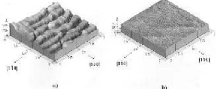
AFM scan of a ZNS-MQW structure grown withN w=
10,
B = 1300nm, T
g = 670
oC with low and high
growth rate is shown in Fig. 1. The morphology for low growth rate exhibits an anisotropic and modulated behavior (Fig. 1a). A strong thickness modulation oc-curs along [110] direction. The root mean square (rms) roughness, dened as the standard deviation of the data, is 5.8nm (approximately 20 mono-layers) and the thickness uctuation, dened as the distance from val-ley to peak, is 35.6nm. For high growth rate (Fig. 1b) the thickness modulation almost disappeared and the surface is essentially at, with a surface roughness less than one mono-layer. The waviness is dependent on the growth temperature, on the growth rate, on the num-ber of wells and on the barrier composition. Reduced number of wells, higher growth temperatures, higher growth rates and barrier compositions grown outside the miscibility gap (
B = 1100 and 1400nm) are
re-quired to keep the morphology of ZNS structures at and without waviness.
Figure 1. AFM image of a ZNS structure with N w = 10, B = 1300nm,Tg= 670
oC with a) low and b) high growth
rate.
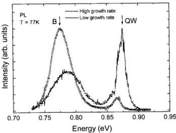
The low temperature PL spectra of ZNS samples grown with N
w = 10,
B = 1300nm, T
g = 670 oC and
with low and high growth rates are shown in Fig. 2. Both PL spectra exhibited a very broad emission band (FWHM = 40meV) below the fundamental quantum well transition (FWHM = 16meV). The intensity ra-tio (I
QW =I
B) between the quantum well peak (labeled
QW) and the broad emission band (B) depends on the number of wells, on the growth temperature, on the growth rate and on the barrier composition. The PL spectra of ZNS samples grown with the same structure but at lower temperatures and lower growth rates were dominated by the emission band B. At T
g = 640 oC
and R= 2:5A/sec. the relative intensityI QW
=I
B was
as low as 0.08. Nevertheless, PL spectra of ZNS sam-ples grown with T
g = 670
oC and R=10A/sec.
exhib-ited higher relative intensityI QW
=I
B of 2.12. The PL
spectra of ZNS structures grown with a xed growth temperature of 670oC, growth rate of 10A/sec. and N
w=10, but with dierent barrier bandgap wavelength,
showed a remarkable increase of the relative intensity
I
QW =I
B as the barrier bandgap wavelength was varied
from 1200 to 1400nm. The broad emission band B was not observed in the PL spectra of ZNS structures with
B = 1400nm and N
w = 5 or N
w = 10. This
behav-ior can be tentatively explained by the use of constant As/P ratio in the wells and barriers (for
B=1400nm)
which is known to reduce the thermal interdiusion of group V species between barriers and wells. Also the barrier composition for
B=1400nm exhibits less phase
separation, due to the miscibilitygap, and consequently reduced alloy compositionuctuation is expected. Both eects result in improved interface quality. This obser-vation was conrmed by AFM and X-ray diraction measurements, where at surface morphologies and in-tense and sharp satellite peaks were obtained in these samples, respectively. However, a further increase in the number of wells toN
w = 15 and N
w = 20 in ZNS
structures grown with
B = 1400nm resulted in
Brazilian Journal of Physics, vol. 29, no. 4, December, 1999 841 X- ray satellite peaks become broader and less intense
and the relative intensity ratioI QW
=I
Bdecreases as N
w
is increased from 15 to 20.
Figure 2. PL spectra of ZNS samples grown with low (cir-cles) and high (crosses) growth rate. The arrows point to the broad band (B) and quantum well peak (QW).
The PL broad band emission B was not detected after the growth of a complete laser structure. The growth time of samples analyzed in this work is typi-cally 40 min. A complete laser structure requires in-stead 3 hours of growth. This behavior may be ex-plained if band B is attributed to defects generated at the interfaces between the tensile strained barriers and the compressive strained wells. During growth of the uppermost layers in the laser structure these defects are healed by the annealing process and the interface qual-ity is improved. This results in the total suppression of the emission band B and a reduction of the well PL linewidth.
Double crystal X-ray diraction, using Cu??1 radi-ation and (400) reection, showed a strong inuence of the growth rate on the structural properties of these samples, as shown in Fig. 3. The satellite intensities are strongly increased and became sharper for the sample grown at the higher growth rate. The n = +1 satellite diraction linewidth is reduced by a factor of 1.9 when the growth rate is increased from 2.5 to 10A/sec. These results suggest the presence of a strong interface undu-lation and/or alloy uctuations in the structures grown at lower growth rate. Similar results were obtained for ZNS samples grown at dierent growth temperatures. Structures grown with lower temperatures (640oC)
ex-hibited reducedI QW
=I
Bvalues, low intensity and broad
x-ray diraction satellites when compared to samples grown at higher temperatures (670oC).
Figure 3. CuK1, (400) X-ray diraction pattern of samples
grown with a) low and b) high growth rates.
High quality ZNS structures, dened by a at mor-phology, a highI
QW =I
B ratio in the PL spectrum and
a high intensity and sharp x-ray diraction satellites, were obtained with high growth temperatures and high growth rates. When the growth temperature is low-ered the mobility of atoms at the surface is reduced. As a result, there is a reduction in the strain relax-ation mechanism and less undulrelax-ation is expected to oc-cur [4]. However, lowering the growth temperature in-creases the miscibilitygap of the quaternary alloy and a phase separation can take place [2,3], resulting in com-position uctuations of the tensile barrier layers. On the other hand, higher growth rate also decreases the mobility of atoms at the surface [9]. The interplay of these three mechanisms dominates the morphology and the optical and structural properties of ZNS structures. The predominance of one mechanism over the others is strongly inuenced by the growth technique, amount of strain in the layers and the growth parameters.
Figure 4. Pulsed light-current characteristics at T = 22oC
of several quaternary MQW ZNS ridge lasers, grown with
Tg= 670 oC,
Nw= 10 and B = 1400nm. The inset shows
842 WilsondeCarvalhoJr. et al.
Ridge waveguide ZNS laser structures emitting at 1.55m, withN
w = 10, grown at 670
oC and at a high
growth rate, exhibited excellent electro-optic teristics. Fig. 4 shows pulsed light-current charac-teristics of several ridge waveguide ZNS lasers, with
B = 1400nm. The threshold current ranges from
23 to 26mA, with an external quantum eciency of 0.2mW/mA. Similar results were obtained for struc-tures grown with barriers of
B = 1300nm and
B =
1200nm.
IV Conclusions
We presented an eective method to improve the ma-terial quality of InGaAsP/InGaAsP/InP MQW ZNS structures. Higher growth temperatures, higher growth rates and alloy compositions lying outside the miscibil-ity gap are needed to dramatically suppress the wavy layer growth and to improve structural and optical characteristics of ZNS structures. ZNS ridge waveg-uide lasers exhibited excellent electro-optic characteris-tics with low threshold currents and high output exter-nal dierential eciencies.
Acknowledgements
We wish to thank Mr. Helio Gazetta Filho and Mr.
Luis Carlos S. Vieira for technical support on crystal growth and device processing.
References
[1] R. People and J.C. Bean, Appl. Phys. Lett. 47, 322
(1985)
[2] B. de Cremoux, P. Hirtz and J. Ricciardi, Inst. Phys. Conf. Ser. N.56, 115 (1980).
[3] G. B. Stringfellow, J. Electronic Materials, 11, 903
(1982).
[4] A. Ponchet, A. Le Corre, A. Godefroy, S. Salaun, and A. Poudoulec, J. Crystal Growth,153, 71 (1995).
[5] H. Chen, R. M. Feenstra, R.S. Goldman, C. Silfve-nius and G. Landgren, Appl. Phys. Lett.72(14), 1727
(1998).
[6] R.W. Glew, K. Scarrot, A.T.R. Briggs, A.D. Smith, V.A. Wilkinson, X. Zhou and M. Silver, J. Crystal Growth,145, 764 (1994).
[7] R. Bhat, M. A. Koza, D. M. Hwang, K. Kash, C. Caneu and R. E. Nahory, J. Cryst. Growth,110, 353 (1991).
[8] C. G. Van de Walle, Physical Review B,39(3), 1871
(1989).
[9] N. Y. Jin-Phillipp, F. Phillipp, T. Marschner and W. Stolz, J. of Material Science: Materials in Electronics