Optical Absorption and Emission of
Nanomaterials Integrated in One Dimensional
Photonic Crystals
Report presented to apply for PhD degree by:
Olalla Sánchez-Sobrado
PhD Advisor:
Hernán Ruy Míguez García
Tutor of the University of Seville:
Diego Gómez García
Department of Physics of Condensed Matter
University of Seville
Institute of Materials Science of Seville
Spanish National Research Council
For the ones who had a notion, a notion deep inside that ain´t no sin you
be glad you´re alive
.Quisiera agradecer, en primer lugar, a mi director de tesis. No hay mucha gente que pueda presumir de admirar a su jefe.Yo sí. Gracias por todo lo que has hecho por mí, que es mucho más que dirigirme la tesis. Tu ejemplo ha sido una gran motivación para mí a lo largo de estos cuatro años. Gracias por celebrar más que nadie mis buenos momentos y por apoyarme en los malos. Tus enseñanzas y consejos me los llevaré siempre, y vaya a dónde vaya podré decir con mucho orgullo que yo fui doctoranda del gran Hernán Míguez.
También quiero agradecer al segundo autor (a veces creo que el primero) de esta tesis: Mauricio Calvo. Todo este trabajo habría sido absolutamente imposible sin tu ayuda, y buena parte de lo que soy te lo debo a ti. Gracias por toda la paciencia que has tenido conmigo, por solucionar todas mis crisis con un “Enter” y por decir “¡Ahí voy!”…y venir, siempre.
A lo largo de estos cuatro años, mis compañeros del grupo de Materiales Ópticos Multifuncionales han estado SIEMPRE TODOS disponibles para CUALQUIER cosa que haya necesitado. Por eso, desde Agus hasta Alberto, esta tesis lleva un pedacito de cada uno de ellos. Especialmente de Silvia, que me enseñó a apilar las dichosas nanopartículas, y de Gabriel, a cuya colaboración debo algunos de mis resultados más importantes. A Mari Carmen le quiero agradecer todo su apoyo y cariño desinteresado en los momentos en los que más lo he necesitado, y también en los que menos lo he merecido. Eres muy fuerte, muy profesional y muy inteligente, y estoy segura de que tendrás una gran tesis. Y no me quiero olvidar de Curro, qué gran lección de dedicación y compañerismo nos has dado. Por último (lo bueno se hace esperar), Nuri (H, por supuesto). Juntas empezamos esto de la tesis hace cuatro años, juntas hemos quemado todas las fases y juntas estamos llegando al final. Gracias por haber sido una gran compañera y por haber estado siempre ahí. ¡Pórtate bien!
Quiero agradecer a Manuel Ocaña y Nuria Núñez por sus importantes aportaciones en esta tesis. Algunos de los resultados más destacados de mi trabajo no habrían sido posibles si no contáramos con los nanofósforos sintetizados por ellos. Sus consejos y su disponibilidad han sido una constante estos cuatro años.
A Luis Liz-Marzán y su equipo del Grupo de Química Coloidal de la Universidade de Vigo, quiero agradecer la confianza depositada en nuestro proyecto y su importante aportación mediante la síntesis de las nanopartículas de oro.
También quiero agradecer, muy especialmente, a Alejandro Giacomotti, Ariel Levenson y a toda la gente del Laboratoire de Photonique et de Nanoestructures (CNRS, Francia), por su cálido recibimiento durante mi estancia en París y todo el esfuerzo empleado en sacar adelante las medidas de las propiedades angulares de la luminiscencia de los resonadores conteniendo nanofósforos.
Gracias a Martyn Pemble y Kevin Thomas, del Tyndall Institute (UCC, Ireland), con quienes se llevó a cabo la infiltración de los espejos de Bragg con GaAs.
Quiero agradecer a Diego Gómez que haya aceptado ser mi tutor en la Universidad de Sevilla, por su ayuda desinteresada, su disponibilidad y el gran interés que ha mostrado siempre por mi trabajo.
enseñarme Sevilla, hacerme reír y por tantas cosas que ha hecho por mí. A Sonia, eres un ejemplo par mí por tu paciencia, compañerismo y alegría. A Anita (aunque sea técnico), que nos endulza a todos. A Víctor y Marcela que siempre me han cuidado. A David Abad que tanto me ha hecho reír. Y a los chicos guapos del instituto: los catalíticos Luisito, Óscar y muy especialmente Yesid. Algún día cumpliremos nuestra amenaza de mandar esto de la ciencia al carajo y nos retiraremos a cuidar la huerta de nuestras respectivas familias, y nos visitaremos mutuamente y tomaremos café…aunque hasta entonces, querido Yesid, los vagabundos como tú y como yo hemos nacido para correr.
Mi agradecimiento al Ministerio de Ciencia e Innovación por la concesión de una beca de formación de personal investigador.
A Rosa. Querida compañera de piso, amiga del alma y hermana para siempre. ¡Cuánto he aprendido de ti! Gracias por haberme hecho mejor, más fuerte, más segura y más feliz.
Al frente galaico popular de Sevilla, es decir, la Yols, la Mari, y la Maria Teresa Garea Pereira. Desde el día que llegué a Sevilla hace cuatro años habéis sido mi familia, me habéis cuidado y me habéis hecho reír. Gracias por haberme dejado formar parte de vuestras vidas y por haberos superapuntado a la mía.
Y a toda la muchachada con la que he compartido ratos realmente grandiosos estos cuatro años. Conchi, Ricardo, Loretta, Fran, Martina, Francesco, Chantal, Julia, Pau y Marco… (seguro que me olvido de gente, ¡lo siento!). Es gracias a vosotros que para mí Sevilla tiene y tendrá siempre un color muy espacial.
A miña curmá Sara. Nunca tiven a oportunidade de darche as grazas. Pois grazas. Por todo. Por coidarme tanto, por todo o teu apoio, polo teus miles de apuntes, pola túa infinita paciencia e pola cantidade de horas que botaches escoitando (aturando) tódalas miñas lerias diarias. Bótoche moito de menos prima. E o resto de tolos do monte da condesa e resto do universo polarizado en directa: o meu queridísimo Pacucho de Caldas, sweet Pilar , Martinsiño, o meu análogo do ICMM, Pablo, moita leria, moito chisme e moita viaxe. E tamén Silvia máis Miki, Kike, Vicente, Xullo, Xurxo, Óscar, Carlos, Sonia, Sofía, Gonzalo, David bizcochito, Carolina, Sara González, Maite (outra vez)...¿olvídome de alguén?. Seguro que sí. Ó voso carón empezou todo isto. Contei co voso apoio e axuda dende o primeiro día que entrei pola porta da facultade. A vosa amizade é moi valiosa para min e foi o voso exemplo o que me fixo, en parte, chegar ata aquí…non importa ónde estea cada un ...¡Verémonos sempre na nosa Compostela!
Ás miñas familias, polo seu apoio e polo interese mostrado en esas cousas do demo chamadas cristais fotónicos. En especial ó meu irmán Fran, que foi o meu primeiro profe de física e “arreglaproblemas” en xeral e a persoa que máis me fai encender o ordenador para explicarlle que raios fago en Sevilla.
Dende pequena aprendín que para lograr os meus obxetivos hai que facer dúas cousas. Primeiro soñalos e despois traballalos. Se son forte, é porque me fixeron forte. E se cheguei ata aquí, e se teño que chegar máis lonxe, pois será polos valores que me inculcaron, polos principios que me fan ser o que son. Por iso quero dedicar esta tese as dúas persoas que máis admiro no mundo, os meus pais Germán e Salomé.
Non des a esquecemento
da inxuria o rudo encono;
esperta do teu sono
fogar de Breogán.
Contents
Chapter I. Introduction.
1. One dimensional photonic crystals (1DPCs)……….…….pag 1 2. Porous 1DPCs………..……..pag 7 3. 1DPCs made of nanoparticles………..………...…….pag 10 4. Motivation and objectives of this thesis……….………..…….pag 14 5. References……….…….…..pag 16
Chapter II. Techniques of fabrication of nanoparticle one dimensional photonic crystals.
1. Introduction………..……….………….pag 21 2. Spin coating ……….………..………..……..pag 22 2.a Nanoparticle 1DPCs built by spin coating ……….……….…pag 22 2.b Optical and structural quality……….……pag 25 2.c Control of the optical response……….…..pag 28 2.d Analysis of the spin parameter………pag 29 3. Dip coating ……….……….………..….pag 33 3.a Nanoparticle 1DPCs built by dip coating ……….……….….…pag 33 3.b Optical and structural quality……….pag 35 3.c Control of the optical response………..…….pag 37 4. Conclusions……….…...….pag 41 5. References………..…….pag 42
Chapter III. Control and optimization of the optical properties of nanoparticle one dimensional photonic crystals.
2.b Optical response to environmental changes……….….…..pag 48 2.c Resonant cavities………..……….pag 50 3. Engineering higher order diffraction .……….………pag 51 4. Flexible nanoparticle 1DPCs with tailored response ………..……..pag 53 4.a Infiltration with Polycarbonate……….….…………pag 54 4.b Infiltration with PDMS………..………..pag 59 5. Conclusions………pag 62 6. References………..……pag 63
Chapter IV. Infiltration of high refractive index materials in nanoparticle one dimensional photonic crystals.
1.Introduction……….pag 65 2.Metalorganic chemical vapor deposition of III-V semiconductors………pag 66 3.Gallium arsenide infiltration of nanoporous multilayers..………..pag 69 3.a Structural properties……….……….pag 69 3.b Optical properties………..pag 72 3.c Analysis of the results………pag 74 4.Conclusions………..pag 78 5. References……….………..pag 79
Chapter V. Modification of the optical absorption of metallic nanoparticles integrated in one dimensional photonic crystals.
6. References………...pag 100
Chapter VI. Control of the photoluminescence of nanophosphors integrated in one dimensional photonic crystals.
1. Introduction………..…….….….pag 103 2. Preparation and structure of nanoparticle based optical cavities…..………pag 104 3. Tailoring the emission bands …………..……….……...pag 107 3.a Enhancement and suppression of photoluminescence bands………..…..pag 107 3.b Modification of the relative intensities of photoluminescence bands………..…pag 109 4. Response to environmental changes………...pag 111 4.a Sensing liquids………..…….pag 111 4.b Sensing gases………..………….…..pag 114 5. Angular emission properties……….pag 118 6. Conclusions ………..……..pag 124 7. References………..………pag 125
Appendix. Synthesis of nanoparticles………...…pag 127
General conclusions……….………..…….pag 131
Resumen en español. Emisión y Absorción Óptica de Nanomateriales Integrados en Cristales Fotónicos Unidimensionales.
1. Introducción……….….……….…pag 135 2. Técnicas de fabricación de cristales fotónicos unidimensionales basados
en nanopartículas……….….pag 142 3. Control y optimización de las propiedades ópticas de cristales
fotónicos unidimensionales………..pag 147 4. Infiltración de materiales de alto índice de refracción en cristales
6. Control de la fotoluminiscencia de nanopartículas dopadas con tierras raras e integradas en cristales fotónicos unidimensionales .………..pag 164
7. Conclusiones………...………pag 173 8. Referencias………..……….…...pag 175
Abbreviations………...pag 179
Chapter I
Introduction
1. One dimensional photonic crystals.
Figure 1. Diagrams of one (a), two (b) and three (c) dimensional photonic crystals.
spontaneous emission and localization phenomena in these materials, respectively. Photonic bands are the result of plotting the dispersion relation between the
frequency ω and the wave vector
k
of the allowed energy states of the crystal ω=ω(k
). This relation, in a homogeneous medium, is independent of the direction of propagation and is ω=(c/n)|k|, where n is the refractive index on the medium (real and constant in the range in which the material presents no absorption) and c is thelight speed in vacuum. In periodic structures, ω=ω(
k
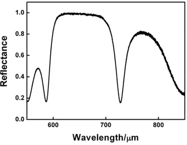
) depends on the direction of propagation.A one dimensional photonic crystal is a multilayer structure that presents a periodic modulation of the refractive index in only one direction of the space.1 The band structure corresponding to a 1DPC is showed in Figure 3(a). In the figure, the frequency ω of the photons is expressed in dimensionless units, where d is the lattice parameter of the periodic structure. The wave vector, k, is given as k d. The case illustrated in the figure is that in which the propagation of light is perpendicular to the periodicity. The energy ranges in which the existence of optical modes in the crystal is forbidden are known as photonic band gaps. As a consequence, the electromagnetic radiation with this frequency would be reflected by a real structure with the same periodicity. This can be seen by comparing the band structure of Figure 3(a) with the reflectance spectrum plotted in Figure 3(b) corresponding to a 1DPC of ten unit cells and the same periodicity. In this spectrum, the secondary Bragg diffraction orders can be clearly distinguished. In a first approximation, the maximum of order m is placed at λ0/m, where λ0 is the spectral position of the lower energy diffraction order.
Figure 3. (a) Band structure corresponding to a one dimensional photonic crystal. (b) Reflectance spectrum corresponding to 1DPC of 5 unit cells with the same periodicity. The colored bands indicate the photonic band gaps of the structure.
On the other hand, the group velocity, vg, can be calculated from the slope of
k
k
v
g∂
∂
=
ω
(
)
(1)Thus, the optical modes propagating at frequencies in which the slope is small present low group velocity and the light will be confined at those spectral regions. These phenomena take place at the band gap edge of 1DPCs or at resonant modes corresponding to optical cavities obtained breaking their periodicity. Thus, at these resonant regions, the electromagnetic density of modes (DOM) present their maximum values.4 The DOM can be calculated as the inverse of the group velocity:
ω
ω
ω
ρ
∂ ∂ = = 1 ( ) )( k
vg
(2)
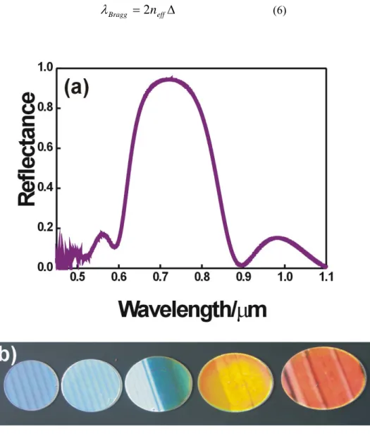
The orders of diffraction are usually called Bragg peaks. An example of a Bragg peak corresponding to a 1DPC is plotted in Figure 4(a). If the Bragg peak is placed at the visible range of the electromagnetic spectrum, the 1DPC displays bright colors, see Figure 4(b). Some basic features of the Bragg peak can be analyzed with approximate formulas. For instance, its spectral position λBragg can be estimated
through Bragg’s law combined with Snell’s law:
θ
λ
2 2sin
2
Δ
−
=
effB
n
m
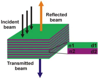
(3)where m is a diffraction order, Δ is the thickness of the basic structural unit or unit cell, θ is the angle between the direction of incidence and the direction normal to the surface of the structure and neffis the effective refractive index of the structure:
2 1 2 2 1 1 d d d n d n neff + +
=
(4)
Where n1 and n2 are the refractive index of each one of the two types of layers
and d1 and d2 their respective thickness. Thus, λBragg can be modified by changing
these parameters. The position of the Bragg peak λBragg can be calculated through the
Equation 3. Thus, the first order diffraction (m=1) at normal incidence occurs at:
Δ
=
effBragg
2
n
λ
(6)
The simplest way to construct these structures is alternating layers of materials with different refractive index. To get these ensembles of high optical and structural quality, each layer must be uniform and the refractive index contrast between layers of different materials must be high, in order to attain a wide reflection peak. The optical response depends on three parameters: the refractive index of the components, the thickness of each type of layer and the number of layers. The Bragg peaks observed in the reflectance spectra are wider and more intense as the number of cells increases.5 On the other hand, the thickness and the refractive index of the materials forming the unit cell determine the position of the reflectance maximum.
A wide variety of techniques based on physical vapour deposition methods are used to fabricate these Bragg reflectors with very good results.6 These procedures consist in heating a material until its temperature of evaporation is reached and make it condense on a substrate forming a film. Then, the sample is kept below its temperature of fusion. Thus, resistant and durable coatings of metal oxides with good optical properties are obtained. The main inconvenient of this kind of techniques is the request of high temperatures to evaporate. A very important parameter to control along the process is the thickness of the film, which can be determined by optical methods like ellipsometry, reflectance and transmittance. Another important factor to take into account is the type of substrate. An inappropriate substrate leads to a bad adherence of the film. Thin films built by physical vapour deposition present dense microstructure, with low or null porosity. This assures the stability against environmental changes. This is an advantage for their use as passive optical elements, but renders them useless as base for sensors because their optical properties are not modified in response to environmental changes. On the other hand, methods based in the wet deposition of sol-gel precursors of inorganic compounds on flat substrates, as
2. Porous 1DPCs.
For applications as detectors of liquids and gases, it would be desirable to build 1DPCs presenting optical response to environmental changes. Porous structures in which the control of optical properties depends on the control of the composition and the morphology and size of the pores, have been proposed with this aim.9 Recently, a wide variety of porous Bragg stacks have been realized following methods based on electrochemical etching, physical vapor deposition at glancing angle or wet deposition. These materials have several applications in fields such as biological and chemical sensing,10, 14 detection and recognition,15 photovoltaics,16 conducting17 and
photoconducting coatings,18radiation shielding,19,20 or light emission
.21
The electrochemical etching is a methodology in which tubular pore structures are constructed by selective elimination of well-defined regions of a metal wafer, normally silicon or alumina, through the combination of oxidation and latter dissolution in an acidic electrolyte. The size and shape of the pores, and therefore the optical response of the structure, are determined by the modulation of a current density applied to the substrate. Thus, the refractive index of a specific layer of the structure is determined by the thickness of the pore walls. The fabrication process is schematized in Figure 5(a). The first porous multilayer was made of silicon. A single silicon wafer was made porous by passing an anodic current in a fluorhydric acidic solution, obtaining pores with size comprised between 2 nanometers and a few microns depending on the charge density, the concentration of the ion fluoride and the doping level of the silicon wafer.22 As an example of this kind of structures, Figure 5(b) shows a scanning electron microscopy (SEM) of the cross section of a 1DPC made by alternating porous silicon layers of different porosity.23 Its reflectance spectrum is plotted in Figure 5(c). Alumina is another important material used to fabricate porous 1DPCs by electrochemical etching.24 In a first electrochemical step, a mirror-polished aluminum substrate is anodized in an acidic solution to generate a surface array of regularly arranged stem pores. In a second anodic step, the current is sinusoidally modulated to generate a pore structure from the seminal pores previously obtained. The Figure 5(d) displays a SEM image of a cross section of a 1DPC made of alumina.13 The three transmittance spectra plotted in Figure 5(e) coorespond to porous alumina mutilayers composed by 15, 30 and 45 unit cells (spectra 1, 2, and 3 respectively). The advantage of the electrochemical etching techniques is the great reproducibility and accuracy of the pore modulation achieved, whereas the main drawback is that it can only be applied to materials that can be obtained in the shape of conducting wafers.
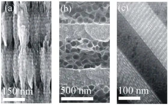
methodology to fabricate porous 1DPCs. It combines the traditional thin film vacuum deposition with a particular geometry in which the substrate is tilted with respect to the line connecting the target and the substrate.25 The final ensemble is provided with highly accessible and tunable interconnected porosity. This technique allows controlling the refractive index along the stacking direction. Bragg stacks can be attained by deposition of one or two different materials. In the first case, the contrast between the refractive index of layers forming the unit cell can be reached through the control of the angle of the deposition since this determines the porosity. By using only one material, bulk properties are not affected. Titanium dioxide and indium tin oxide have been used to obtain conductive26 or photoconductive17 porous Bragg mirrors. In Figure 6(a) a SEM image of the cross section of a TiO2 1DPC built using
this technique is shown.10 An example of deposition of two different materials is that in which SiO2 and TiO2 multilayers are fabricated keeping the interconnected porous
structure between layers.27 This technique allows controll the size and the density of the interstitial sites very precisely for each layer individually.
The methods based on wet deposition also assure fine control over the properties of porous structures and the reproducibility of the whole pore system. These methods consist in the sequential deposition of two types of porous layers from solution-derived precursors by spin28 or dip coating.31 The materials that have been used for this purpose are supramoleculary templated metal oxides, clays and nanoparticles of different sort. The experimental conditions of the deposition and the composition of the liquid precursor dispersions yield control over the pore size distribution and overall porosity of the mesoporous networks.
Figure 6. Scanning electron microscopy images of the cross section of porous one dimensional photonic crystals made of (a) titanium dioxide by physical vapor deposition at glacing angle (b) laponite – TiO2 system.(c) supramolecularly templated layers of SiO2 and TiO2. (Images extracted from references 10, 28, 29).
Clay Bragg Stacks (CBS)28 are made alternating layers of laponite (a synthetic philosilicate clay of empirical formula Na0.7[(Si8Mg5.5Li0.3)O20(OH)4]) and metal
oxides porous layers as TiO2. These two materials present a high contrast between
adsorbents, ion exchange materials and catalysis. On the other hand metal oxides are used to stack meso-ordered porous metal oxide thin films by using an organic template. The choice of the metal oxide precursor, the solvent and the organic templating agent are crucial factors to determine the pore size and the morphology of the network. The number of materials that can be shaped as mesostructured thin films, hence used to build 1DPCs, is limited practically to SiO2 and TiO2.29- 31
Alcoholic solutions of titanium (IV) or silicon (IV) compounds are usually chosen as precursors and cationic surfactant like CTAB (cetyl trimethyl ammonium bromide) or block copolymers like Pluronics F127 are used as templates. After the deposition of the precursors by spin or dip coating, the polymer is removed by a heating treatment that consolidates the inorganic wall. These Bragg stacks are foreseen to be used as base materials in optical sensing due to their narrow pore size distribution. A cross section of one of these structures is shown in the SEM image of Figure 6(c).35
3. 1DPCs made of nanoparticles.
In this thesis, we present a complete study of the structural and optical properties of 1DPCs made of nanoparticles, as well as of their capacity to modify the optical properties of several nanomaterials of different morphologies. This ability of the nanoparticle Bragg mirrors to adapt to any arbitrary shape of the guest material is a key factor that leads to preserve the optical quality of the periodic structures studied along the research work herein presented. Methods based in deposition of sol-gel precursors are usually chosen to obtain a rich variety of metal oxide colloidal suspensions controlling the size and the shape of the resulting particles. This kind of materials presents the optimal features to attain 1DPCs with the required structural and optical properties. In order to construct the Bragg mirror, nanoparticles are sequentially deposited from their colloidal suspensions (preferably in alcoholic media). To assure a good optical response, the variation of the refractive index between the different materials forming the 1DPC must be high and a smooth interface between layers is necessary. The surface charge and the pore size distribution of the particles play an important role in the stacking and in the interpenetration of the layers respectively. Some metal oxide colloids are commercial while others particles have to be synthesized taking into account the different experimental parameters that influence the size and the shape of the obtained nanoparticles. Due to their high refractive index contrast, the most employed nanoparticles are those of SiO2 and TiO2.32 Other examples include the stacking of
alternated porous layers of SnO2 and Sb:SnO2 with SiO2 nanoparticles.33 Another
with different aggregation state were stacked to generate the refractive index contrast.34
One dimensional photonic crystals made of nanoparticles of SiO2 and TiO2
were firstly fabricated within the Multifunctional Optical Materials group by Silvia Colodrero et al.32 In this work, our group presented a Bragg stack made by alternated deposition of these colloids under strict control of the aggregate state by using the spin coating technique. The resulting layers are well packed but keep a highly accessible and interconnected porosity. This structure is schematized in Figure 7(a). The study of the optical and structural properties of these photonic crystals, as well as their application to modify optical absorption and photoluminescence of different materials integrating them, are the main objectives of this thesis. Preliminary studies about the environmental response of different porous 1DPCs have proved their potential as base materials for detection of gases and liquids.32,35,36 It has been also demonstrated that nanoparticle one dimensional photonic crystals amplified the conversion of the efficiency of solar energy into electricity in certain type of photovoltaic cells.16
The starting materials are colloidal suspensions of both types of particles in methanol using concentrations comprised between 1 and 6 % wt. This solvent was chosen because no coagulations was observed in the suspension when it is prepared in this way37 and at the same time the liquid is volatile enough to completely leave the structure during the formation process. SiO2 colloids were purchased from
Dupont (Ludox TMA, Aldrich), and TiO2 crystallites were synthesized using a
procedure described in the Appendix. The most important parameter that influences on the uniformity of layers is the size of the particles. The control over the size distribution and the amount of aggregates is crucial to obtain smooth interfaces between the two types of layers in order to attain a good optical response. The monodispersity of nanoparticles was checked using photocorrelation spectroscopy.35 Monomodal distributions of TiO2 nanocrystals and SiO2 colloids were attained as
shown in Figure 7(b). One of the advantages that these materials present is the sequentiality of depositions. When a layer is formed, the next can be immediately deposited, no intermediate treatment being necessary. The Figure 7(c) shows a scanning electron microscopy image of the cross section of a twelve unit cell 1DPC made of nanoparticles of oxides of titanium and silicon. Uniformity in the long range can be clearly appreciated, while the different morphology of the spherical SiO2 and
the more irregular TiO2 particles is evident in Figure 7(d), which is a magnification of
7(c). The two types of interfaces can be also distinguished. The surface between neighboring layers is flat when SiO2 nanoparticles are deposited onto the more
compact TiO2 crystallites and is more diffuse when the opposite occurs, since TiO2
crystallites are then able to penetrate a few nanometers into the larger pores of the layers of SiO2 colloids. This does not significantly affect the fact that a high dielectric
contrast between neighboring layers can be attained.
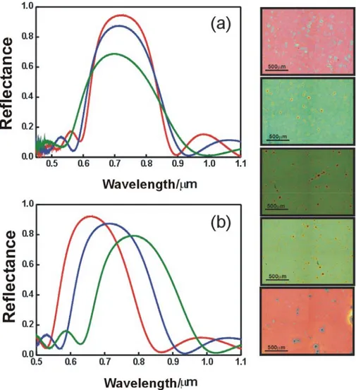
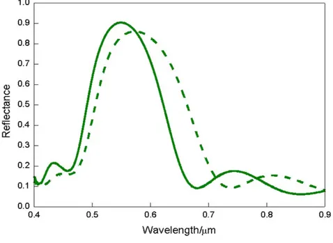
As it was described before, the intensity of the Bragg peak of a 1DPC depends on the number of cells forming the structure. The evolution of the optical response of a SiO2-TiO2 nanoparticles multilayer with the number of deposited cells is shown in
Figure 8(a). The observed Bragg maxima, associated to the presence of a photonic band gap in the direction normal to the layers, are more intense and narrower as the number of unit cells increases.4 In the figure, red, blue and green lines corresponds to 5, 4 and 3 unit cell stacks respectively. Intense (up to 90%) and wide Bragg reflection peaks are observed, which is a direct consequence of the large refractive index contrast between the SiO2 nanoparticle layers and the TiO2 nanocrystal ones. The way
Figure 8. Evolution of the reflectance spectrum of a SiO2-TiO2 nanoparticle multilayer with the number of cells. Red, blue and green lines correspond to 5, 4, and 3 unit cell multilayers respectively (a) and with the lattice parameter (b); red, blue and green lines corresponds to silica concentrations of 3, 3.5, and 4 % wt respectively. (c) Optical microscope pictures of multilayers with different lattice parameters.
3.5, and 4 % wt., respectively, the concentration of the suspension of titania as well as the rest of the experimental parameters remaining fixed. This is the proof that nanoparticles 1DPCs with high reflectivities can be attained over the whole UV-Vis-IR electromagnetic spectrum. Optical microscope images are displayed in left panel of Figure 8 to show the different colors reflected by nanoparticle 1DPCs with different lattice parameters. The refractive index of TiO2 and SiO2 nanoparticle
respectively) and the air of the pores. It can be estimated by fitting the optical reflectance spectra using a scalar wave approximation.38,39 The calculated values are 1.74 for titania and 1.24 for silica layers. This implies that the pore volume fraction in the films is around 45% in both cases,40 as calculated using the Bruggeman equation:
0
2
2
2 22 2 2 2 2 2
=
+
−
+
+
−
a a a d d dff
n
n
n
n
ff
n
n
n
n
[7]
Where n is the average refractive index of a layer, nd is the refractive index
corresponding to the bulk material, na is the refractive index of the air filling the
pores and ffd and ffa the corresponding filling factors. These equation will be used
for most calculations of porosity from average refractive index values presented in this thesis.
4. Motivation and objectives of this thesis.
One of the most developed areas in nanotechnology in the last years is that of nanoparticles that present resonant absorption or optical activity. On one hand, several examples have been reported about the properties of metallic nanoparticles with a well defined resonant absorption peak placed at the visible range due to the excitation of the localized surface plasmon. This kind of particles has been applied in fields such as catalysis41, sensing42 or optics.43 The optical absorption is normally controlled through the surrounding material44 or by controlling the size and shape of the particles.45 On the other hand, there are lots of examples of luminescent nanoparticles with applications in fields as light emitting diodes (LEDs),46 sensing47 and bio-labelling.48 Again, the optical properties of these nanoparticles are usually controlled by controlling their size and shape.49 The available emission patterns of nanoparticles range from white light emission of certain semiconductor quantum dots,50 to the narrow, atom-like ones of rare earth based nanophosphors.51
observed, probably because this kind of structures presents weak field localization at their resonance frequencies. Also, sharp and intense optical absorption fluctuations have been predicted for Bragg mirrors containing arrays of noble metal particles.54 But most multilayers studied so far show several difficulties to host nanoparticles with different shape and size.
In the case of luminescent particles, there are various reported works about the infiltration of quantum dots in different photonic structures and the modification of their luminescence.55,56 However, only two examples has been reported about the integration of rare earth doped nanophosphors in three dimensional photonic crystals.57,58 In these experiments, significant modification of the luminescence lifetime was observed at photonic band gap frequencies. However, no selective and controlled suppression or enhancement of luminescence bands has been observed by integration of the nanophosphors in optical resonant cavities. Again, this is probably due to the difficulty to embed particles with arbitrary shape and size in periodic structures with the capacity to localize light.
Therefore, the motivation of this thesis was to build photonic structures provided with high optical quality, and hence, with the ability to confine light strongly in the frequencies of their resonances and with the capacity to host either absorbing or optically active nanoparticles with different shape and size, to significantly modify their optical properties. By infiltration in nanoparticle one dimensional photonic crystals, the controlled and selective amplification of the absorption of gold nanoparticles and of the photoluminescence of nanophosphors has been observed for the first time. The objectives of the thesis herein presented, entitled
“Optical Absorption and Emission of Nanomaterials Integrated in One Dimensional Photonic Crystals”, were:
− To sstudy of techniques of fabrication of nanoparticle 1DPCs and to analyze the dependence of both optical and structural properties on the experimental parameters. The results of this analysis are presented in Chapter II.
−To fabricate porous multilayers by using the studied procedures. Optimize the optical properties of porous multilayers over the range NIR-Vis-UV. These results are explained in Chapter III.
−To infiltrate nanoparticle 1DPCs with materials of high refractive index. The obtained results are explained in Chapter IV.
5. References.
[1] J.D. Joannopoulos, R.D. Meade, J.N. Winn. “Photonic Crystals: Molding the Flow of
Light”, Princeton University Press, Princeton, 1995.
[2] E.Yablonovitch. “Inhibited spontaneous emission in solid-state physics and electronics”,
Physical Review Letters, 58,1987, 2059.
[3] S.John. “Strong localization of photons in certain disordered dielectric superlattices”,
Physical Review Letters, 38,1987, 2486.
[4] J.M. Bendickson, J.P. Dowling, M. Scalora. “Analytic expressions for the electromagnetic
mode density in finite, one dimensional, photonic band gap structures”, Phys.Rev.E, 53, 1996,
4107.
[5] A. Yariv, P. Yeh. “Optical Waves in Crystals”, John Wiley and Sons Inc., ISBN
0-471-43081-1. 2003
[6] Macleod, H. A., “Thin Film Optical Filters”, 4rd Edition, Published by Institute of Physics
Publishing, London, 2001.
[7] S. Rabaste, J. Bellessa, A. Brioude, C. Bovier, J.C. Plenet, R. Brenier, O. Marty, J. Mugnier, J. Dumas. “Sol-Gel fabrication of thick multilayer applied to Bragg reflectors and
microcavities”, Thin Solid Films, 416, 2002, 242.
[8] R.M. Almeida, A. S. Rodrigues. ”Photonic bandgap and structures by sol-gel processing”,
Journal of Non-Crystalline Solids, 326, 2003, 405.
[9] N. Hidalgo, M. E. Calvo, H. Míguez. "Mesostructured Thin Films as Responsive Optical
Coatings of Photonic Crystals", Small, 5, 2009, 2309.
[10] J.J. Steele, A.C. van Popta, M.M. Hawkeye, J.C. Sit, M.J. Brett. “Nanostructured
gradient index optical filter for high-speed humidity sensing” Sensors & Actuators , 120,
2006, 213.
[11] K. A. Killian, T. Böcking, J.J. Gooding, Chem. Commun.2009, 630.
[12] S.Colodrero, M.Ocaña, A.R.González-Elipe, H.Míguez.“Response of nanoparticle one
dimensional photonic crystals to ambient vapour pressure” Langmuir, 24, 2008, 9135.
[13] D.L. Guo, L.X. Fan, F.H. Wang, S.Y. Huang, X.W. Zou, “Porous Anodic Aluminum
Oxide Bragg Stacks as Chemical Sensors”, J. Phys. Chem. C, 112,2008, 17952.
[14] B.V. Lotsch, G.A. Ozin. “Clay Bragg Stack Optical Sensors”, Adv. Mater, 20, 2008,
4079.
[15] L. D. Bonifacio, D. P. Puzzo, S. Breslav, B. M. Willey, A. McGeer, G. A. Ozin. “Towards the Photonic Nose: A Novel Platform for Molecule and Bacteria Identification”
[16] S. Colodrero. A. Mihi. L. Haggman, M. Ocaña, G. Booscholoo, A. Hagfeldt, H. Míguez, “Porous One-Dimensional Photonic Crystals Improve the Power-Conversion Efficiency of
Dye-Sensitized Solar Cells”, Advanced Materials, 21, 2009, 764.
[17] M.F. Schubert, J.Q. Xi, J.K. Kim, E.F. Schubert. “Distributed Bragg reflector consisting
of high- and low-refractive-index thin film layers made of the same material” Appl. Phys.
Lett, 90, 2007,141115.
[18] M.E. Calvo, S. Colodrero, T.C. Rojas, M. Ocaña, J.A. Anta, H. Míguez.
“Photoconducting Bragg Mirrors based on TiO2 Nanoparticle Multilayers” Adv. Func. Mater.
18, 2008, 2708.
[19] P. Kurt, D. Banerjee, R.E. Cohen, M.F. Rubner, “Structural color via layer-by-layer
deposition: layered nanoparticle arrays with near-UV and visible reflectivity bands” J. Mater.
Chem.,19, 2009, 8920.
[20] M.E. Calvo, O. Sánchez-Sobrado, G. Lozano, H. Míguez, "Molding with nanoparticle based One Dimensional Photonic Crystals: A Route to Flexible and Transferable Bragg
Mirrors of High Dielectric Contrast.". J. Mater. Chem. 19, 2009, 3144.
[21] F. Scotognella, D.P. Puzzo, A. Monguzzi, D.S. Wiersma, D. Maschke, R. Tubino, G.A.
Ozin. “Nanoparticle One-Dimensional Photonic-Crystal Dye Laser” Small, 5, 2009, 2048.
[22] R. Herino, G. Bomchil, K. Barla, C. Bertrand, JL. Ginoux. “Porosity and Pore-Size
Distributions of Porous Silicon” J. Electrochem. Soc., 134, 1987, 1994.
[23] J. J. Saarinen, S. M. Weiss, P. M. Fauchet and J. E. Sipe. “Reflectance analysis of a
multilayer one-dimensional porous silicon structure: Theory and experiment” J. Appl. Phys,
104, 2008, 013103.
[24] W. J. Zheng, G. T. Fei, B. Wang, Z. Jin, L. D. Zhang. “Distributed Bragg reflector made
of anodic alumina membrane”, Materials Letters, 63, 2009, 706.
[25] M. J. Brett, M. M. Hawkeye. “Materials science - New materials at a glance” Science,
319, 2008, 1192.
[26] J.J. Steele, A.C. van Popta, M.M. Hawkeye, J.C. Sit, M.J. Brett. “Nanostructured
gradient index optical filter for high-speed humidity sensing”, Sensors & Actuators, 120,
2006, 213.
[27] L. González-García, G. Lozano, A. Barranco, H. Míguez, A. R. González-Elipe. “TiO2
-SiO2 one-dimensional photonic crystals of controlled porosity by glancing angle physical
vapour deposition” J. Mater. Chem, 20, 2010, 6408.
[28] B.V. Lotsch, G.A. Ozin. “Photonic Clays: A New Family of Functional 1D Photonic
Crystals” ACS nano, 2, 2008, 2065,
[29] M.C. Fuertes, G. J. A. A. Soler-Illia, H. Míguez, “Process for Preparing Multilayers with
(WO2008034932), Priority date 18/09/2007
[30] S.Y. Choi, M. Mamak, G. Freymann von, N. Chopra, G.A. Ozin. “Mesoporous Bragg
stack color tunable sensors”, Nano Lett, 6, 2006, 2456.
[31] M.C. Fuertes, F.J. López-Alcaraz, M.C. Marchi, H.E. Troiani, G.J.A.A. Soler Illia, H. Míguez. “Photonic Crystals from Ordered Mesoporous Thin-Film Functional Building
Blocks” Adv. Funct. Mater. 17, 2007, 1247.
[32] S. Colodrero, M. Ocaña, H. Miguez. “Nanoparticle base done dimensional photonic
crystals”. Langmuir, 24, 2008, 4430.
[33] D. P. Puzzo, L. D. Bonifacio, J. Oreopoulos, C. M. Yip, I. Manners, G. A. Ozin. “Color
from colorless nanomaterials: Bragg reflectors made of nanoparticles” J.Mater.Chem,19,
2009, 3500.
[34] M.E. Calvo, S. Colodrero, T.C. Rojas, M. Ocaña, J.A. Anta, H. Míguez,
“Photoconducting Bragg Mirrors based on TiO2 Nanoparticle Multilayers”Adv. Func. Mater,
18,2008, 2708.
[35] M. C. Fuertes, S. Colodrero, G. Lozano, A.R. González-Elipe, D. Grosso, C. Boissière, C. Sánchez, G. J. de A. A. Soler-Illia,H. Míguez, “Sorption properties of mesoporous
multilayer thin films” J. Phys. Chem. C, 112, 2008, 3157.
[36] S. Colodrero, M. Ocaña, A.R. González-Elipe, H. Míguez, “Response of
nanoparticle-based one-dimensional photonic crystals to ambient vapor pressure” Langmuir, 24, 2008,
9135.
[37] I. M. Thomas. “Single-Layer TiO2 and Multilayer TiO2-SiO2 Optical Coatings Prepared
from Colloidal Suspensions”Appl. Opt 1987, 26, 4688.
[38] K. W. K. Shung, Y. C. Tsai. ”Surface Effects and Band Measurements in Photonic
Crystals” Phys. ReV. B, 48, 1993, 11265.
[39] A. Mihi, H. Míguez. “Origin of light-harvesting enhancement in
colloidal-photonic-crystal-based dye-sensitized solar cells” Phys. Chem. B, 109, 2005, 15968.
[40] H. C. van de Hulst. “Light Scattering by Small Particles” Dover Publications: New
York, 1981.
[41] R.M. Crooks, M. Zhao, L. Sun, V. Chechik, L.K. Yeung, “Dendrimer-encapsulated metal
nanoparticles: Synthesis, characterization, and applications to catalysis”, Acc. Chem. Res, 34,
2001, 181.
[42] D.J. Maxwell, J.R. Taylor, S. Nie. “Self-assembled nanoparticle probes for recognition
and detection of biomolecules”, J. Am. Chem. Soc, 124,2002, 9606.
[43] E. Hutter, J.H. Fendler. “Exploitation of localized surface plasmon resonance”, Adv.
[44] K. L. Kelly, E. Coronado, L. L. Zhao, G. C. Schatz, “The optical properties of metal
nanoparticles: The influence of size, shape, and dielectric environment ” J. Phys. Chem. B
2003, 107, 668.
[45] K. A. Willets, R. P. Van Duyne. “Localized surface plasmon resonance spectroscopy and
sensing ”Ann. Rev. Phys. Chem.2007, 58, 267.
[46] V. L. Colvin, M. C. Schlamp, A.P. Alivisatos. “Ligth Emitting-Diodes made from
Cadmium Selenide Nanocrystals and a Semiconductor Polymer” Nature, 370, 1994, 354.
[47] I. L. Medintz, H. T. Uyeda, E. R. Goldman, H. Mattoussi, “Quantum dot bioconjugates
for imaging, labelling and sensing“, Nature Mat, 4, 2005, 435.
[48] J. K. Jaiswal, H. Mattoussi, J. M. Mauro, S. M. Simon “Long-term multiple color
imaging of live cells using quantum dot bioconjugates”, Nature Biotech. 21, 2003, 47.
[49] X. Peng, L. Manna, W. Yang, J. Wickham, E. Scher, A. Kadavanich, A. P. Alivisatos,
“Shape control of CdSe nanocrystals”, Nature,404,2000, 59.
[50] M. J. Bowers, J. R. McBride, S. J. Rosenthal, “White-light emission from magic-sized
cadmium selenide nanocrystals”J. Amer. Chem. Soc. 127, 2005, 15378.
[51] J. C. Boyer, L. A Cuccia, J. A. Capobianco, “Synthesis of colloidal upconverting NaYF4
: Er3+/Yb3+ and Tm3+/Yb3+ monodisperse nanocrystals”. Nano Lett.7, 2007, 847.
[52] F. García-Santamaría, V. Salgueirino-Maceira, C. López, L.M. Liz-Marzán, “Synthetic
opals based on silica-coated gold nanoparticles” Langmuir, 18, 2002, 4519.
[53] D.Y. Wang, V. Salgueiriño-Maceira, L.M. Liz-Marzán, F. Caruso. “Gold-silica inverse
opals by colloidal crystal templating ”Adv. Mater.2002, 14, 908.
[57] E. Lidorikis, S. Egusa, and J.D. Joannopoulos. “Effective medium properties and
photonic crystal superstructures of metallic nanoparticle arrays” J. Appl. Phys, 101, 2007,
054304.
[58] P. Reithmaier, G. Sek1, A. Löffler, C. Hofmann, S. Kuhn, S. Reitzenstein, L.V. Keldysh, V.D. Kulakovskii, T.L. Reinecke, A. Forchel, “Strong coupling in a single quantum
dot-semiconductor microcavity system”. Nature 432, 2004, 197.
[59] P. Lodahl, A. F. van Driel, I. S. Nikolaev, A.Irman, K. Overgaag, D. Vanmaekelbergh, W. L. Vos. “Controlling the dynamics of spontaneous emission from quantum dots by photonic
crystals” Nature, 430,2004, 654.
[57] M. Aloshyna, S. Sivakumar, M. Venkataramanan, A. G. Brolo, F. C. J. M van Veggel,.
“Significant suppression of spontaneous emission in SiO2 photonic crystals made with Tb3+
-doped LaF3 nanoparticles”, J. Phys. Chem. C, 111, 2007, 4047.
[58] Z. X. Li, L. L. Li, H. P. Zhou, Q. Yuan, C. Chen, L. D. Sun, C. H. Yan. “Colour
Chapter II
Techniques of fabrication of nanoparticle one dimensional
photonic crystals
1. Introduction.
All the samples prepared and analyzed to obtain the results presented in this thesis are based in multilayers formed by nanoparticles of SiO2 and TiO2. To design
the optical response of these Bragg stacks is necessary to control both the refractive index and the thickness of the layers. These materials were first constructed by Silvia Colodrero et al. by using a spin coating process.1 In this work different photonic crystals with different optical response were attained by changing the concentration of the precursor suspensions and keeping fixed the angular spinning speed. However, the range of suitable concentrations to obtain photonic crystals with good quality is narrow. For high values, aggregates of nanoparticles are formed leading to a bad adherence of the films. For low concentrations, the substrate is not totally covered. Also, it is very difficult to precisely control the optical response of the structures only by changing the concentration of the precursor suspensions.
of SiO2 and TiO2 on flat glass substrates. The optimal parameters to build multilayers
with a minimum number of defects and with the desired optical response are found for both studies. The control over the parameters of the fabrication process, acceleration ramp and final rotation speed in the case of the spin coating, as well as the concentration of precursor suspensions and the extraction speed in the case of the dip coating, is crucial to control the quality and the optical response of 1DPCs.
2. Spin coating.
2.a Nanoparticle 1DPCs built by spin coating.
Spin coating is a procedure used to apply uniform thin films on flat substrates. Briefly, an excess amount of precursor solution or suspension is placed on the substrate, which is then rotated at high speed in order to spread the fluid by centrifugal force. Rotation is continued while the fluid spins off the edges of the substrate, until the desired thickness of the film is achieved. The solvent employed is usually volatile, and simultaneously evaporates. For higher angular speed, a thinner film is attained. The thickness of the film also depends on the concentration of the precursor solution or suspension, as well as on its viscosity.
Figure 1. Description of the spin coating process. (a) Deposition of the precursor suspension on the still substrate. (b) Acceleration. In this phase the excess amount of suspension is removed and the film begins to slim. (c) Rotation. The slimming continues when the final rotation speed is reached. (d) The evaporation of the solvent is the main factor in the formation of the film during the last part of the process.
Being the spin coating the main method employed to prepared most structures analyzed in this research work, a thorough study of the spin coating protocol was performed. A detailed analysis of the effect of the spin coating parameters,
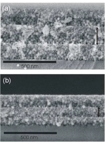
Figure 2. FESEM images showing the cross section of periodic nanoparticle multilayers obtained at final speeds of (a) 2500 rpm and (b) 6000 rpm.
A total of 42 samples, of six layers each one of them, were prepared by an alternated deposition of TiO2 and SiO2 nanoparticle suspensions. The synthesis of
nanoparticles is described in the Appendix. These sols were deposited over glass substrates using a spin coater (Laurell WS-400E-6NPP) in which both the acceleration ramp and the final rotation speed could be precisely determined. The first layer was deposited using 250 ml of SiO2 sol and the substrate was tilted and
final speed) is completed in 60 seconds. Sequentially, another layer of a different type of nanoparticle is deposited following the procedure described above. The process is repeated until a total of six layers have been deposited. Final speed was chosen between nominal values of 2000 and 8000 revolutions per minute (rpm) and accelerations were selected between nominal values of 1950 and 13650 rpm s-1. The precursor suspensions were diluted in methanol to 4 and 2 % wt. for TiO2 and SiO2
particles respectively. These concentrations remain constant along the experiments. The structure of the different sintered 1DPCs was studied by observing the cross sections of multilayers deposited under different conditions. Field emission scanning electron microscopy (FESEM) images of two cleaved films made of three SiO2-TiO2
bilayers are displayed in Figure 2. As expected, increasing the final rotation speed diminishes the final thickness of the layers, as Figures 2(a) and 2(b) illustrates. In each case, the black arrows indicate the thickness of the unit cell. In these examples, the same SiO2 and TiO2 solutions were deposited and spun at 2500 rpm and 6000
rpm, unit cells of 180 nm and 120 nm being obtained respectively. The acceleration used was 8450 rpm s-1 in both cases.
2.b Optical and structural quality.
further improves if steep accelerations ramps are employed. Variations of the reflectance maximum intensity can be directly related to the presence of imperfections in the sample, since they give rise to diffusely scattered light that is actually removed from the reflected and transmitted beams. In this case, regardless of the uniformity of the response, the height of the peaks is never below 60% for 6 layer (3 unit cell) films.
Figure 3. Specular reflectance spectra taken from 1DPCs deposited using different spin coating conditions: (a) ω= 2000 rpm, γ= 3250 rpm s-1; (b) ω= 8000 rpm, γ= 3250 rpm s-1; (c) ω= 2000 rpm, γ= 8450 rpm s-1; (d) ω= 8000 rpm, γ= 8450 rpm s-1. In each case, spectra taken at different distances from the centre of the sample are plotted using a different line colour: ▬ 0 mm, ▬2 mm, ▬4 mm, ▬6 mm,
Figure 4. Optical microscopy images of different multilayer built at different final and ramp accelerations. Each pair of images were obtained from multilayers deposited at the same final rotation speed and accelerations of γ=11050 rpm s-1 and γ=1950 rpm s-1(top and bottom images in each case, respectively). (a) ω=8000 rpm, (b) ω=6000 rpm and (c) ω=2000 rpm.
Among the defects typically observed in films deposited from particle suspensions by spin coating, the most relevant ones are those known as striations and comets. Striations are radially oriented undulations of the film, and are the result of the rotation of a surface cell pattern.3,4 Such pattern may be present in any liquid film with one of its surfaces exposed to air as a result of the Marangoni effect.5 In such films, surface tension gradients, which in this case could be originated by local fluctuations of the suspended particle concentration or the temperature, induce fluid flows that set up a cell surface pattern. Rotation of such pattern gives rise to the elongation of the cells, an effect that is more intense as the distance from the centre increases, which yields the striation pattern typically observed in spin coated films.6
of images of 1DPCs prepared using ω=8000 rpm and ω=6000 rpm and accelerations of γ=11050 rpm s-1 (top images) and γ=1950 rpm s-1 (bottom images). In all cases, the density of comets increases dramatically when slow ramps are used. In this case, the amount of comets observed in films deposited simultaneously onto similar substrates and from the same precursor suspension, changes with the conditions used in the spin coating protocol, as it can seen by comparing each pair of images shown in Figures 4(a), 4(b), and 4(c). This indicates that such comets originate during fluid flow and solvent evaporation from the rotating film. In the case of an impulsive acceleration (higher γ values) solvents abandon the suspension rapidly, which causes an abrupt increase of viscosity and a decrease of fluid flow. Under these conditions, aggregation of the nanoparticles may be hindered and, consequently, the formation of comets.
2.c Control of the optical response.
Figure 5. Reflectance spectra obtained at acceleration ramps (a) γ=1950 rpm s-1 and (b) γ=11050 rpm s-1. Final speeds, ω (rpm) = 2000 (blue), 2500 (red), 3000 (black), 3500 (green), 4000 (cyan), 6000 (pink), 8000 (yellow).
2.d Analysis of the spin parameter
.
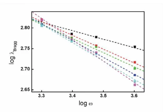
Figure 6. Bragg peak spectral position (nm) versus ramp stage acceleration γ. The different lines correspond to different final rotation speedsω (rpm): 2000 (black), 2500 (red), 3000 (green), 3500 (blue), 4000 (cyan), 6000 (pink), 8000 (yellow).
plotted in Figure 6 can be used as a guide to attain 1DPCs of high structural quality whose Bragg peak precisely matches the desired wavelength range. Hence, it can be seen that worse optical quality is attained when the slowest ramps (γ=1950 rpm s-1 and γ=3250 rpm s-1) are used, independently of the nominal final rotation speed. As the slope of the ramp increases, so too does the optical quality of the multilayer. In general, the optical quality attained is good when ω and γ take values above 2500 rpm and4550 rpm s-1 respectively. Regarding the control of the optical response, the results summarized in Figure 6 clearly show that when the final rotation speed is reached fast, be it due to the large γ (γ>5850 rpm s-1) or the low nominal ω (ω<3000 rpm) employed, then the position of the specular reflectance Bragg peak maximum,
Figure 7. Log-Log graph representation of the Bragg peak position against final rotation speed. Best fitting obtained in ramp, γ (rpm.s-1): 1950 (black), 3250 (red), 4550 (green), 5850 (blue), 8450 (cyan), 11050 (magenta).
b is a constant known as the spin parameter, with a typical value of 0.5 for newtonian fluids. The solutions of nanoparticles used to construct the structures of this study are considered as newtonian fluids, which are defined as fluids whose stress versus strain rate curve is linear, being the viscosity the constant of proportionality. In his work, Meyerhofer also introduced the concept of cross-over point, which is the time at which the contribution of fluid flow becomes, due to the increasing viscosity of the forming film, so small that equals that of evaporation. The relation T~ω-0.5 is obtained considering that thinning is first and foremost caused by viscous fluid flow due to spinning and, to a minor extent, by solvent evaporation. Recently, Birnie et al. have theoretically demonstrated that this expression is only valid if the cross-over point is reached when the fluid is already rotating at the final nominal speed ω.8 After their study, if most film thinning takes place during the ramp stage, i.e., the cross-over point occurs before the nominal ω is reached, then the spin parameters should be
Figure 8. Spin parameter, b, versus ramp acceleration, γ.
average refractive index and the lattice constant of the ordered multilayer. The former is determined by the porosity and refractive index of the layers, which in turn depend on the composition, shape and packing of the nanoparticles that form them, hence being independent of ω and γ. The latter, however, is determined by the thickness of the two types of nanoparticle layers (SiO2 and TiO2), which should depend on ω
thorough the expression T=ω-b. Assuming that both kinds of layers depend on ω on a similar way, then the Bragg peak maximum is expected to follow the expression
λBragg~ω-b. So, it can be estimated the spin parameter of these multilayers by plotting
λBragg versus ω
-b in a logarithmic graph for each acceleration ramp used in these
experiments and extracting their slope. Curves are shown in Figure 7 only for
final speed. In those cases, it is observed a clear correlation between λBragg and ω. Thus, it can be established that precise control of the lattice parameter is attained by varying exclusively ω if the thinning of each layer in the 1DPC due to fluid flow caused by substrate rotation is still larger than the thinning due to solvent evaporation when the final rotation speed is reached. On the contrary, low values of b are attained when small γ are used. For those cases it is observed that λBragg does not depend strongly on ω (see Figure 6). In such cases, the final thickness of each layer in the 1DPC is achieved before the substrate reaches the final rotation speed, i.e., the cross-over occurs during the ramp stage.
3. Dip coating.
3.a Nanoparticle 1DPCs built by dip coating.
The spin coating technique allows building multilayers under strict control over Bragg peak position and over the optical and structural quality, as seen in the previous section. As a consequence, most structures analyzed in this research work have been satisfactorily designed and constructed using this method. Another procedure susceptible of allowing the formation of thin nanoparticle films onto flat substrates is dip coating. Several multilayers have been prepared with this method in order to analyze their optical and structural quality. The results obtained are presented in this section.
The dip coating technique is a method employed to create uniform thin films9,10 that can be deposited onto flat or cylindrical substrates. The dip coating procedure is completed in five steps.11 The first is the immersion. The substrate is immersed in the solution or suspension of the coating material at a constant speed. Then, the start-up, in which, the substrate remains inside the solution for a while and then starts to be pulled up at a constant speed. The third phase is the deposition. A thin layer is deposited on the substrate while it is being lifted. The speed determines the thickness of the coverage (faster extraction speeds leads to thicker films). During
Figure 9. Scheme of the formation of a nanoparticle 1DPC by dip coating.
The dip coating technique, applied to the construction of nanoparticle 1DPCs, is schematized in Figure 9 for the colloidal suspensions used in the experiments of this study. The concentrations of the precursor suspensions were 3.5 % wt. for TiO2
nanocrystals, while concentration of SiO2 particles were 2, 2.5, 3, 3.5, 4, 4.5 % wt.
The following values for the extraction speed were used: 1.25, 1.5, 1.75 and 2 mm/s. The procedure, explained before, was repeated alternating the solutions of SiO2 and
TiO2 nanocrystals to build the whole multilayer.
3.b Optical and structural quality.
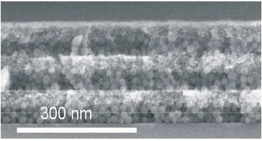
All the samples studied in this section were composed by three unit cells, easily distinguished in the FESEM image of Figure 10. In the image, all the features of nanoparticle 1DPCs observed in the structures constructed following the spin coating procedure are clearly shown. The SiO2 spheres are perfectly distinguished of the
smaller TiO2 nanocrystals with irregular shape. The two types of boundaries typical
of these Bragg stacks can be observed. The border is much smoother when the SiO2
nanoparticles are deposited onto the TiO2 layer. This is because the pores of the latter
are small comparing to the size of the SiO2 spheres, which prevents them to penetrate
the TiO2 layer.
Figure 10. FESEM image of a three unit cell nanoparticle one dimensional photonic crystal. The SiO2 nanospheres are clearly distinguished of the smaller TiO2 nanocrystals
Figure 11. Optical microscopy images 11(a) and 11(b) show surfaces of two multilayers that differ only in the concentration of silica, which are 3.5% wt. and 4.5% wt. respectively. Their corresponding sets of reflectance spectra, 11(c) and 11(d), were obtained from 15 different measurements of the reflectance in 15 different point of each sample. For those samples, in figures 11(e) and 11(f) the position of the maximum of reflectance spectra (units of energy) versus the point, in mm, where these measurements were taken, are plotted. Error bars are the standard deviation of the average value of five measurements taken in a perpendicular line to the direction of growth and separated by 4 mm.
respectively, keeping fixed the rest of experimental parameters. The homogeneous coloured background is a proof of the good uniformity that layers present. This uniformity is only broken by particle aggregates. Most defects are very small and their effect in the uniformity of layers is almost not appreciable. However, larger defects can be easily differentiated. These are minor in number, but their big size influences the uniformity of layers and can lead to dispersion in the measurement of the position of the Bragg peak, deteriorating the optical quality of the materials. By studying carefully both pictures, it can be appreciated that aggregates are slightly bigger when the concentration of the silica suspension is higher and, consequently, the dispersion observed in the Bragg peak position is also going to be higher. To check this, 15 reflectance spectra from 1 mm2 area spots placed at the nodes of a virtual rectangle net and separated from each other by 4 mm were collected. In every case the total area studied was 3 cm2. These spectra are plotted in Figures 11(c) and 11(d). The multilayers were made from suspensions of silica with concentrations of 3.5 and 4.5% wt respectively. The spectral position of the Bragg peak practically does not change in the multilayer with smaller defects, while certain dispersion was measured for some spots in the sample in which the size of aggregates is higher. But, even this dispersion is low since the total area analyzed is very large. The multilayer obtained is endowed with high uniformity. The homogeneity depends on the size of defects and therefore the concentration of silica in the precursor suspension. This dependence is confirmed after carefully studying the Figures 11(c) and 11(d). In Figures 11(e) and 11(f), five Bragg peak position values are plotted, in units of energy for the sake of clarity, since the observed change is then independent of the spectral range in which it takes place, versus the position at which the measurement was taken, separated by 4 mm along the direction of growth. Each data is in turn the average value of five measurements taken in a perpendicular line to the direction of growth and also separated by 4 mm. Error bars are the standard deviation of these values, so their lengths should be interpreted as a measurement of the deviation of each Bragg peak position from its average value and, hence, as an estimation of the uniformity of the optical response of the crystal.
3.c Control of the optical response.
controlling the spin coating parameters i.e., final rotation speed and acceleration ramp. On the other hand, the thickness of films built by using dip coating depends on several parameters as the extraction speed, the concentration and the viscosity of the fluid precursors, the surface tension, the boiling point of the precursor solvent or the kind of substrate employed. In this section, a study about how to control the optical response of nanoparticle Bragg stacks constructed by dip coating is presented. Only two parameters are modified: the extraction speed and the concentration of the SiO2
precursor suspension.
As it was explained before, a change in the thickness of the unit cell leads to a change of the position of the Bragg peak, that is, different colours are reflected by the structure. The figure 12(a) displays a photograph of five samples with an area of 3 cm2 prepared by dip coating. The reflectance spectra of this kind of structures are shown in figure 12(b). These multilayers differ only in the concentration of the precursor suspension of SiO2 nanocolloids in methanol, while extraction speed
remains constant. From left to right, the concentrations used were 2, 2.5, 3, 4, and 4.5 % wt. By increasing this concentration, the thickness of silica layers becomes larger and the position of Bragg peak red-shifts. By using this method, multilayers with optical response over the whole range of visible spectrum were constructed, as the set of spectra of Figure 12(b) confirms. This dependence is also shown in the graph plotted in Figure 12(c). The position of Bragg peak linearly increases with the concentration of the silica solution for a fixed withdrawal speed of 1.5 mm/s.
To study the dependence of the optical response with the deposition parameters, different multilayers were constructed modifying the concentration of the SiO2 precursor suspensions and the available withdrawal speed. Results are
other by 4 mm. As well as before, error bars are obtained from the standard deviation and should be again interpreted as a measure of the homogeneity of layers. It can be seen that the error bars are shorter if multilayers are built from precursor silica suspension with lower concentration. It should be noted that the violet line is drawn without error bars. This is because the system used to measure reflectance spectra, consisting in a microscope attached to a spectrophotometer, introduces noise in measurements of spectra under 400 nm and it is not possible to distinguish accurately positions of Bragg peaks in different points of the sample. However, due to the small size of defects of this set of multilayers made from the lowest concentration silica suspension, it can be predicted that the length of bars must be very short. Clearly, it can be concluded that the position of the Bragg peak is not dependent on the withdrawal speeds in the available range.
Figure 13. Bragg peak spectral position versus extraction speed. The different lines correspond to different concentrations of SiO2suspensions: 4.5 (black), 4 red), 3.5 (green), 2.5 (blue) and 2 wt % (violet). Error bars are the standard deviation of the average value of 25 measurements taken in different points of each sample.