Photoluminescence Properties of Te Doped AlGaAsSb Alloys
D. O. Toginho Filho, I. F. L. Dias, J. L. Duarte, E. Laureto,
Departamento de F´ısica, Universidade Estadual de Londrina, CP 6001, CEP 86051-970, Londrina-Paran ´a, Brazil
and Jean C. Harmand
CNRS, Laboratoire de Photonique et de Nanostructures, Route de Nozay, 91460 Marcoussis, France
Received on 2 August, 2005
A detailed study of the photoluminescence properties in undoped and Te-doped AlGaAsSb alloys lattice matched to InP is presented. Photoluminescent temperature and excitation intensity dependences are employed to discuss the origin of the dominant transition and the influence of the presence of Al and Te on the fluctuation of the electrostatic potential in the epitaxial layers. The behavior of PL dominant transitions is associated with the quasi-donor-acceptor-pair (QDAP) model at a low temperature interval. The temperature dependence of photoluminescence intensities showed characteristics similar to those observed for amorphous semiconductors and disordered superlattices. The presence of two V elements, or the presence of Sb in the ternary and quaternary (III)-III-V-V alloys, causes a reduction in photoluminescence intensity temperature dependence, when compared to (III)-III-III-V alloys.
I. INTRODUCTION
Recently, there has been great interest in the materials belonging to the group of III-V antimonide family such as GaAsSb and AlGaAsSb alloys lattice matched to InP due to its applications in heterojunction structures employed in elec-tronic and optoelecelec-tronic devices in the range of 1,0µm and 2,0µm [1-8]. As different semiconductor materials [9-11], the GaAsSb and AlGaAsSb alloys present fluctuation of the elec-trostatic potential in the epitaxial layers due to compositional inhomogeneity resulting from miscibility gap [10]. Sponta-neous ordering in different planes in GaAsSb alloys prepared by different growth techniques [12,13] has also been reported. Nominally undoped GaAsSb shows non-excitonic resid-ual acceptor impurity [14], related to native defects such as gallium vacancies and gallium on antimony sites (VGaGaSb) [15-17], with concentrations of 1016cm−3. PL measurements on undoped GaAsSb/InP as a function of the temperature and excitation intensity at low temperatures were used by Yu et al [10] to identify a high intensity peak in the GaAsSb layer as a donor-acceptor pair (DAP) [18] transition associated with potential fluctuations in agreement with the quasi-donor-acceptor-pair (QDAP) model [10,19]. In doped and compen-sated materials, the random distribution of donor and acceptor impurities [20,21] also causes a fluctuation of the electrosta-tic potential in the epitaxial layers. Consequently, the random impurity potential disturbs the conduction and valence band edges and the conduction and valence energies are distorted by the random potential. Thus the behaviour of PL transi-tions can be explained by the QDAP model [10]. In undoped quaternary AlGaAsSb alloys lattice matched to InP, the PL spectra can also be explained by the QDAP model [22]. The presence of aluminum in the quaternary alloy increases the fluctuation of the electrostatic potential in the epitaxial layers as compared to the fluctuation current in the ternary GaAsSb alloys [22].
In vertical-cavity surface-emitting layers devices (VC-SELs), a mirror reflectivity exceeding 99% and a low elec-tric perpendicular resistance are required for n-type and
p-type Bragg mirrors. The high reflectivity is accomplished by employing high refractive contrast material systems such as AlGaAsSb/AlAsSb [8] and GaAsSb/AlAsSb [23]. However, these systems present a high band discontinuity, which is un-favorable to the current flow through the heterointerfaces [5]. Then the low electrical resistance requires a relatively high doping level. Therefore, the study of the optical properties of GaAsSb and AlGaAsSb doped alloys is very interesting for the technology of fabrication of structures as VCSELs.
Te is the most common n-type dopant employed in ternary and quaternary arsenide-antimonide alloys [5,8,24,25]. It is possible to obtain high doping levels in GaAsSb, AlGaAsSb and AlAsSb alloys by using the Sb2Te3source [3]. However, despite the large interest on the doped AlGaAsSb alloys, a more systematic study of the influence of electrostatic poten-tials and the effect of the presence of Al and Te on the optical properties of Te doped AlGaAsSb alloys has not been found in the literature yet [26,27].
In this work, the optical properties of Te doped AlGaAsSb layers lattice matched to InP with increasing doping concen-trations are analyzed. The photoluminescence (PL) as a func-tion of temperature and excitafunc-tion power is used to investi-gate the origin of the dominant PL peak in the PL spectra and the influence of aluminum and tellurium on the poten-tial fluctuation in the quaternary layers. Two ternary GaAsSb alloys: one nominally undoped and the other Te doped with a doping level of≈3x1018cm−3– typical value employed in GaAsSb/AlAsSb [23]and AlGaAsSb/AlAsSb [8] Bragg mir-rors – are analyzed to allow a comparison between ternary and quaternary alloys.
II. EXPERIMENTAL DETAILS
der Paw methods. Details of the sample parameters such as al-loy composition and doping levels can be seen in Table I. PL Table measurements were performed in the temperature range of 10 K to 300 K, using the 514.5 nm line of a continuous wave Ar+laser , with different excitation intensities. Temper-ature variation was obtained by a closed-cycle helium cryo-stat. The spectral analysis of the luminescence measurements was carried out by a 0.5 m Jarrel-Ash spectrometer, coupled to a cooled InGaAs photodetector, using the standard lock-in technique.
III. RESULTS AND DISCUSSION
Figure 1 shows the PL spectra of samples with an excita-tion of 532 W/cm2at 10K. The PL peaks of undoped and Te doped ternary alloys are in the lower energy region with dom-inant transitions at 797 meV and 827 meV, respectively. The PL peaks of undoped and Te doped quaternary alloys are in the higher energy region with dominant transitions between 900 meV and 990 meV. The energy shift between ternary and quaternary alloys results from the presence of aluminum in quaternary which increases the forbidden gap [28]. The shift of the PL peaks with increasing doping levels to higher en-ergies results from the penetration of the Fermi level into the conduction band, which is typical for n-type doped semicon-ductor materials [29-31].
FIG. 1: Photoluminescence spectra of GaAsSb and AlGaAsSb sam-ples, obtained at 10 K and laser intensity of 532 W/cm2.
Figure 2 shows the energy of PL peak (Fig. 2a) and the full width at half maximum – FWHM (Fig. 2b) for the doped sam-ples at different doping levels at 10K. The broadening of the emission spectrum in doped samples with increasing doping concentrations is due, at low side energy, to the evolution of impurity levels into the impurity band of impurity states and the transitions involving band tails states [32] resulting from potential fluctuations of band edges caused by the random dis-tribution of charged impurities [26,33] and variations in the al-loy chemical compositions [10]. The higher broadening of the FWHM found in quaternary alloys, when compared to ternary
alloys, results from the higher magnitude of the electrostatic potential fluctuations in samples with Al [22,33,34].
FIG. 2: Donor concentration of PL peak energy (a) and FWHM (b) at 10 K, for GaAsSb and AlGaAsSb samples.
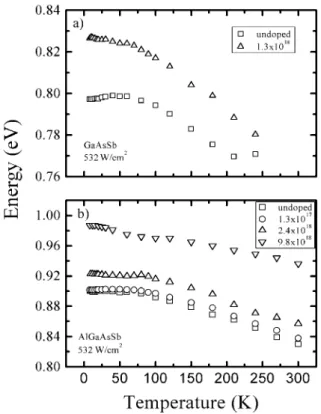
The PL spectra of the Te doped GaAsSb for 1.3x1018cm−3 doping concentration recorded at increasing temperatures from 10K to 210K and of the Te doped AlGaAsSb for 2.4x1018cm−3doping concentration obtained between 10K to 300K temperature range are shown in Fig. 3. The PL spectra show a weak broadening at temperature about 100K , suggest-ing the existence of two recombination channels, one predom-inant at low temperatures (T<100K) and the other dominant at high temperatures.
Table I – Alloy composition and Te doping level in the samples used in this work.
Sample Material Alloy Composition Te Doping Level (cm−3)
x y
#T01
GaAsySb1−y 0.00 0.51
undoped
#66N23 1.3x10¹⁸
#76N46
AlxGa1−xAsySb1−y 0.08 0.51
undoped
#76N43 1.3x10¹⁷
#76N39 2.4x10¹⁸
#76N42 9.8x10¹⁸
FIG. 3: PL spectra obtained at 532 W/cm2laser intensity with tem-perature variation between 10 K and 240 K for GaAsSb samples (a) and between 10 K and 300 K for AlGaAsSb samples (b).
low temperatures. The behavior of the PL peak energy in AlGaAsSb with Te concentration of 2.4x1018 cm−3 is sim-ilar to that observed in the doped ternary alloy with impu-rity concentration of the same order. In the most doped Al-GaAsSb, the behavior of the PL peak is more complex, show-ing a lower variation with the temperature growth. It shows a weak red shift at extremely low temperatures (T<15K), re-maining nearly constant and, finally, dropping with increas-ing temperatures. In general, as the dopincreas-ing concentration in-creases, the anomalous temperature dependence of the dom-inant PL peak energy decreases, as seen in Si doped AlInAs [36]. In this study, the inverted S shaped dependence practi-cally disappears for the doped GaAsSb and doped AlGaAsSb alloys at 2.4x1018cm−3. The weakening of the inverted S –
FIG. 4: Temperature dependence of PL peak energy at several laser intensities for GaAsSb (a) and AlGaAsSb samples (b).
shaped dependence on temperature of the dominant PL peak energy with increasing impurity concentrations cannot be di-rectly associated to a reduction in the disorder of the epitaxial layers. In a process similar to that found for AlInAs:Si [36], the donor binding energy is reduced at high doping levels, causing a higher dopant ionization as the temperature rises. Later in this article, we will discuss the role of the doping level growth and the presence of Al in the order/disorder phe-nomenon.
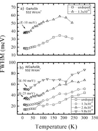
the emission spectrum in an alloy is determined by the im-purity ionization and compositional fluctuations of the epi-taxial layer [38]. The FWHM of the PL peak energy of un-doped GaAsSb shows an increasing broadening (18 meV to 34 meV) in the 10 K to 180 K temperature interval, reaching a maximum at 180K, and a decreasing in higher temperatures. This behavior is similar to that observed for non- intentionally doped In0.52Al0.48As , where the FWHM initially increases due to thermal broadening and, subsequently, decreases due to the gradual ionization of impurities with increasing tempera-tures [37]. The FWHM of doped GaAsSb shows a general be-havior very similar to that observed in the undoped GaAsSb. The FWHM of the doped AlGaAsSb rises in the 10 K to 300 K temperature interval. The presence of Al increases the bind-ing energy in the donor impurity, and the transitions associ-ated with this impurity which is present in the PL spectrum of Te doped AlGaAsSb at room temperature, preventing the FWHM from falling in the temperature interval analyzed.
FIG. 5: Temperature dependence of FWHM peak energy at 532 W/cm2laser intensities for GaAsSb (a) and AlGaAsSb samples (b).
The integrated PL intensity of the dominant transition (I) and the excitation intensity (J) are related by the expression [35]I∝Jk, and for free electron – impurity (electron-acceptor, eA, or donor-hole, Dh) or donor-acceptor pair (DAP) the ex-ponent is less than unity [35]. This analysis was carried out for CdTe, and can be applied to other semiconductor mate-rials with direct band gaps [35,39,40]. Values ofkobtained from the analysis of the integrated PL intensity as function
of intensity excitation can be seen in Table II. These results indicate that the dominant transitions in our PL spectra are re-lated to a band-impurity or donor-acceptor recombination in all samples. In the quaternary doped alloys the acceptor level is probably the same residual acceptor impurity [14] related to native defects such as gallium vacancies and gallium on an-timony sites (VGaGaSb)[16] also found in the GaSb [15] and GaAsSb [17].
Table II – Parameters obtained of the experimental data at 10 K for the PL intensity dependence with the laser intensity, for GaAsSb and AlGaAsSb samples. The fit is carred out using the I =A·
Jkexpression, whereIis the PL peak intensity andJis the laser in-tensity.
Sample Material A k
#T01
GaAsySb1−y
0.13 0.70
#66N23 0.06 0.75
#76N46
AlxGa1−xAsySb1−y
0.26 0.90
#76N43 0.04 0.83
#76N39 0.11 0.67
#76N42 0.06 0.85
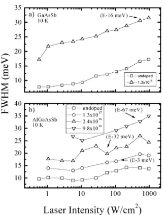
Dominant PL peak (E) energy variations compared to the energies obtained at lower excitation intensities (E0)as a func-tion of power excitafunc-tion at 10 K are shown in Fig. 6. Un-doped GaAsSb PL dominant peak energy shows a blue shift (3.6 meV/decade) as a function of the laser intensity. The be-havior of the PL peak energies for all samples (except the most doped AlGaAsSb) is the same, indicating that the main emis-sion is related to the transition type DAP [35] or QDAP [10]. PL peak energy shifts as a function of excitation intensities of about 3 meV/decade are reported in the literature for strained GaAs0,69Sb0,31 on InP [10], for strongly doped compensated systems [18,41,42] due to the fluctuations of electrostatic po-tential, and also for weak ordered systems [43].
FIG. 6: Laser intensity dependence of peak energy at 10 K for GaAsSb (a) and AlGaAsSb samples (b).
a higher broadening with increasing power excitation (≈5 meV/decade). The growth of FWHM as a function of the dop-ing level indicates the presence of a higher number of ionized impurities, and can be associated to the reduction of the Te donor binding energy involved in the transitions.
Temperature dependence of the integrated PL intensity in the 10 K to 210 K range for the ternary undoped and Te doped ternary alloys are shown in Fig. 8a), and for the undoped and Te doped quaternary alloys in Fig. 8b), at the excitation in-tensity of 532 W/cm2. Due to the presence of localized states, the standard Arrhenius plot cannot be used to fit the integrated PL intensity versus temperature data. The temperature depen-dence of the integrated PL intensity can be fitted well, using an expression deduced from amorphous semiconductors [37,44]:
IPL=I0/[1+A.exp(T/T0)] (1) Where IPLis the normalised intensity of the PL peak, T is the measurement temperature, T0is the characteristic temper-ature associated with the energy depth of localized states, A is the tunnelling factor and I0is the luminescence intensity at the low temperature limit.
The PL intensity as a function of temperature shows a dis-continuity (TD)for all samples similar to that reported in the literature for Al0.5Ga0.5As bulk and disordered superlattices
FIG. 7: Laser intensity of FWHM peak energy at 10 K for GaAsSb (a) and AlGaAsSb samples (b).
[37], for undoped [36,38] and Si doped AlInAs [36] at dop-ing levels between 1x1017cm−3and 4x1018cm−3, and for un-doped GaAsSb and AlGaAsSb [22]. This discontinuity is about TD ≈120 K for the ternary alloys and TD ≈100 K for the quaternary alloys. T0values above and below the discontinuity obtained from the literature and the fitting of the experimental data reported in Figure 8 using the expression (1) are given in Table III.
Table III - Parameters obtained of literature and fitting using theIPL=I0/[1+A.exp(T/T0)]expression in the experimental data for GaAsSb (Fig. 8a) and AlGaAsSb (Fig. 8b) samples, with laser intensity at 532 Watts/cm2.
Alloy Material T0<TD T0>TD Reference
III-III-V undoped
Al0.45Ga0.55As 4.8 - 37
Al0,48In0,52As 17 28 38
Al0,48In0,52As 8 21 36
III-V-V undoped
GaAs0,51Sb0,49 36.6 49.6 22
Al0,07Ga0,93As0,51Sb0,49 30±1 57±2 this work
Al0,12Ga0,88As0,51Sb0,49 20.7 60.3 22
III-III-V doped
AlInAs:Si (1x10¹⁷) 10 37 36
AlInAs:Si (6x10¹⁷) 19 45 36
AlInAs:Si (4x10¹⁸) 40 50 36
III-V-V doped
GaAsSb:Te (1,3x10¹⁸) 38
±1 79±3 this work
AlGaAsSb:Te(1,3x10¹⁷) 48±2 57±2 this work AlGaAsSb:Te(2,4x10¹⁷) 35±2 88±3 this work AlGaAsSb:Te(9,8x10¹⁷) 39±2 124±11 this work
FIG. 8: Temperature dependence of PL intensity for the GaAsSb (a) and AlGaAsSb samples (b) obtained at 532 W/cm2, fitted with equation (1).
temperature variations
Undoped AlGaAsSb samples show a reduction in T0for temperatures below TDwhen Al concentration increases. This behavior can be associated with a growth in binding energy of unknown donor impurity caused by an increase in Al
concen-tration. An increase in donor level energy can have a similar effect to that caused by a decrease in ionization energy with the growth of donor impurities reported by Yoon et al [36] for Si doped AlInAs. In that case, the growth in dopant con-centrations implicates in a higher donor ionization due to the reduction in donor energy and not in disorder. In this work, we believe that a lower donor binding energy of the unknown donor in the GaAsSb gives a similar effect when compared to a higher donor binding energy in AlGaAsSb.
To analyse Te doped GaAsSb and AlGaAsSb epilayers, we need to consider initially that the donor impurity Te (element VI) occupies, preferentially, the As or Sb (elements V) sites in the crystal lattice. For alloys such as AlGaAs and AlInAs, Si (element IV) is the element most employed as donor im-purity, and it occupies, preferentially, the Al, Ga or In (ele-ments III) sites. Table III shows that, for doped AlGaAsSb at temperatures below TD, the T0initially decreases and subse-quently increases with increasing doping levels. This reduc-tion in T0value can be related to a possible contribution of the Te impurities, at moderate concentrations, to the reduction in native defects in alloys of the Sb family, as reported by J.Diaz et al [45] in InGaAsSb alloys prepared by LPE (liquid phase epitaxy). A more systematic work is needed to elucidate this question.
IV. CONCLUSION
alloys show higher potential fluctuation and defect concentra-tions as compared to that observed for ternary alloys type III-III-V. The presence of two V elements or the presence of Sb in alloys (III)-III-V-V reduces the sensibility of the PL intensity to temperature variations. The PL intensity of undoped and Te doped quaternary alloy shows a temperature dependence similar to that found for amorphous semiconductors and dis-ordered superlattices. The presence of Te seems to cause an
increase in the sensibility of the PL intensity to temperature variations at moderate concentrations.
Acknowledgements
The authors wish to thank the financial support granted by the Brazilian agencies CAPES, CNPq, Fundac¸˜ao Arauc´aria and Fundac¸˜ao Banco do Brasil
[1] B. Lambert, Y. Toudic, Y. Rouillard, M. Baudet, B. Guenais, B. Deveaud, I. Valiente, and J. C. Simon, Appl. Phys. Lett.64, 690 (1994).
[2] O.Blum, I.J.Fritz, L.R.Dawson, and T.J.Drummond, Electron. Lett.31, 1247 (1995).
[3] I. F. L. Dias, B. Nabet, A. Kohl, and J. C. Harmand, Electron. Lett.33, 716 (1997).
[4] N.Kuze, H.Goto, M.Matsui, I.Shibasaki, H.Sakaki, J. Cryst. Growth175/176, 868 (1997).
[5] I. F. L. Dias, B. Nabet, A. Kohl, J. L. Benchimol, and J. C. Harmand, IEEE Photon. Technol. Lett.10, 763 (1998). [6] J.C. Harmand, G. Ungaro, I. Sagnes, J.P. Debray, B. Sermage,
T. Rivera, C. Meriadec, J.L. Oudar, R. Raj, F. Olivier-martin, C. Kazmierski, R. Madani, J. Cryst. Growth201/202, 837 (1999). [7] L. Chusseau, G. Almuneau, F. Genty , Recent Research
Devel-opments in Quantum Electronics,Vol. 1, 85 (1999) .
[8] D.O. Toginho Filho, I.F.L.Dias, J.L.Duarte, S.A.Lourenc¸o, L.C.Poc¸as, E.Laureto, J.C.Harmand, Superlattices Microstruct.
31, 277 (2002).
[9] T H Chiu, W.T.Tsang, S.N.G.Chu, J.Shah, and J.A.Ditzenberger, Appl. Phys. Lett.46, 408 (1985).
[10] P.W.Yu, C. E. Stutz, M. 0. Manasreh, R.Kaspi, M.A.Capano, J. Appl. Phys.76, 504 (1994).
[11] B. Shin, A. Lin, K. Lappo, R.S. Goldman, M.C. Hanna, S. Francoeur, A.G. Norman, A. Mascarenhas, Appl. Phys. Lett.
80, 3292 (2002).
[12] J. J. Murgatroyd, A. G. Norman, and G. R. Booker, J. Appl. Phys.67, 2310 (1990).
[13] H R Jen, M. J. Cherng, and G. B. Stringfellow, Appl. Phys. Lett.
48, 1603 (1986).
[14] K.G. Merkel, V. M. Bright, M. A. Marciniak, C. L. A. Cerny and M. O. Manasreh, Appl. Phys. Lett.65, 2442 (1994). [15] P. S. Dutta, H. L. Bhat, and Vikram Kumar, J. Appl. Phys.81,
5821 (1997).
[16] M. Ichimura, K. Higuchi, Y. Hattori, T. Wada, and N. Kitamura, J. Appl. Phys.68, 6153 (1990).
[17] Y.Nakata, T.Jujii, A.Sandhu, Y.Sugiyama, and E.Miyauchi, J. Cryst. Growth91, 655 (1987).
[18] P.W.Yu, C.K. Peng and H.Morkoc¸, J. Appl. Phys. 65, 2427 (1989).
[19] D. R. Chamberlin, S. S. Yi, D. Isaacson, G. Girolami, and N. Moll, Appl. Phys. Lett.83, 2375 (2003).
[20] V.P.Dobrego, I.S.Shlimak, Phys. Stat. Sol.33, 805 (1969). [21] V Swaminathan, V.M.Donelly, and J.Long, J. Appl. Phys.58,
4565 (1985).
[22] D. O. Toginho Filho, I. F. L. Dias, E. Laureto, J. L. Duarte, S. A. Lourenc¸o, L. C. Poc¸as, S. S. Prabhu, and J. Klem, J. Appl. Phys.97, 123702 (2005).
[23] F. Genty, G. Almuneau, L. Chusseau, Wilk, S. Gaillard G. Boissier, P. Grech, J. Jacquet, J. Cryst. Growth201/202, 1024 (1999).
[24] P.S. Dutta, B. Mendez, J. Piqueras, E. Dieguez, and H. L. Bhat, J. Appl. Phys.80, 1112 (1996).
[25] F. Genty, G. Almuneau, L. Chusseau, G. Boissier, J.P. Malzac, P. Salet, and J. Jacquet, Electron. Lett.33, 140 (1997). [26] M.S. Noh, R.D. Dupuis, D.P. Bour, G. Walter, N. Holonyak,
Appl. Phys. Lett.83, 2530 (2003).
[27] C.A. Wang, R.K. Huang, D.A. Shiau, M.K. Connors, P.G. Mur-phy, P.W. O’Brien, A.C. Anderson, D.M. DePoy, G. Nichols, M.N. Palmisiano, Appl. Phys. Lett.83, 1286 (2003).
[28] R. E. Nahory, and M. A. Pollack, Appl. Phys. Lett.27,562 (1975).
[29] Jiang De-Sheng, Y. Makita, K. Ploog, H.J. Queisser, J. Appl. Phys.53, 999 (1982).
[30] Jukka A Lahtinen, Phys. Rev. B33, 2550 (1986).
[31] M. Cardona, K. L. Shaklee, F. H. Pollak, Phys. Rev.154, 696 (1967).
[32] Jacques I. Pankove, Optical Processes in Semiconductors, Dover Publications. Inc., (1971), p10.
[33] E. F. Schubert, I. D. Goepfert, W. Grieshaber, and J. M. Red-wing, Appl. Phys. Lett.71, 921(1997).
[34] E. Iliopoulos, D. Doppalapudi, H. M. Ng, and T. D. Moustakas, J. Appl. Phys.73, 375 (1998).
[35] L.Pavesi, M.Guzzi, J. Appl. Phys.75, 4779 (1994).
[36] S. F. Yoon, Y. B. Miao,K. Radhakrishnan, and H. L. Duan, J. Appl. Phys.78, 1812 (1995).
[37] T. Yamamoto, M. Kasu, S. Noda, A. Sasaki, J. Appl. Phys.68, 5318 (1990).
[38] S.M.Olsthoorn, F.A.J.M Driessen, A.P.A.M. Eijkelenboom, L.J. Giling, J. Appl. Phys.73, 7798 (1993).
[39] T.Schmidt, K.Lischka, and W.Zulehner, Phys. Rev. B45, 8989 (1992).
[40] A. Aydinli, N. M. Gasanly, and K. Goksen, J. Appl. Phys.88, 7144 (2000).
[41] P.W.Yu, J. Appl. Phys.48, 5043 (1977).
[42] H. P. Gislasoh, E, H. Yang, and M. Linnarson, Phys. Rev. B47, 9418 (1993).
[43] M. C. Delong, P. C. Taylor, and J. M. Olson, Appl. Phys. Lett.
57, p620, 1990.
[44] R. A. Street, T. M. Searle, and I. G. Augustine, inAmorphous and Liquid Semiconductors, edited by J. Stoke and W. Brenig (Taylor and Francis, London, 1974), p. 953.
[45] J.Diaz-Reyes, J. L. Herrera-Perez, M. L. Gomez-Herrera, J. A. Cardona-Bedoya, and J. G. Mendoza-Alvarez, Appl. Surf. Sci.

![Table III - Parameters obtained of literature and fitting using the I PL = I 0 /[1+ A.exp(T /T 0 )] expression in the experimental data for GaAsSb (Fig](https://thumb-eu.123doks.com/thumbv2/123dok_br/18981140.457067/6.892.150.767.122.371/table-parameters-obtained-literature-fitting-expression-experimental-gaassb.webp)
