Short Report
S
J. Braz. Chem. Soc., Vol. 22, No. 10, 2013-2017, 2011. Printed in Brazil - ©2011 Sociedade Brasileira de Química 0103 - 5053 $6.00+0.00
*e-mail: [email protected]
Low Temperature Synthesis of CdSiO
3Nanostructures
Leonardo P. Santana, Erick S. de Almeida, Jones L. Soares and Flavio M. Vichi*
Instituto de Química, Universidade de São Paulo, Av. Prof. Lineu Prestes, 748, Bloco 3T, Sala 325, 05508-900 São Paulo-SP, Brazil
Descreve-se a síntese de nanoestruturas de CdSiO3 cristalino como fase única a 580 °C; ao que sabemos, esta é a mais baixa temperatura de formação observada até o presente para este composto. A formação da fase desejada ocorre somente a partir de de 580 °C, já que a 570 °C os picos de difração estão deslocados para menores ângulos em relação ao padrão JCPDS 85-0310. A fonte de silício inluencia diretamente a morfologia do material: Na2SiO3 leva à formação de nanopartículas na forma de agulhas, ao passo que sílica mesostruturada de alta área supericial leva a partículas coralóides. A difratometria de raios X em baixo ângulo mostra que o caráter mesosestruturado da sílica precursora não se mantém no CdSiO3 resultante. A microscopia eletrônica de varredura sugere que, neste caso, haja uma transição da morfologia esférica do precursor para a morfologia em forma de agulhas do material obtido a partir de Na2SiO3. A área supericial do precursor de sílica utilizado tem inluência direta na formação de CdSiO3, pois o uso de sílica comercial de menor área supericial não resulta no produto desejado.
We report the synthesis of single-phase, crystalline CdSiO3 nanostructures at 580 °C; to the best of our knowledge, this is the lowest temperature at which this material is reported to form. The desired phase does not form below 580 °C, since the diffraction peaks are shifted to lower angles in the material treated at 570 °C when compared to JDPDS Card No. 85-0310. The source of silicon has strong inluence on the product morphology: Na2SiO3 yields single-phase CdSiO3 in needle-shaped nanostructures, while high surface area mesostructured SiO2 yields coralloid-shaped particles. Low angle X-ray diffractometry reveals that the mesostructured nature of the silica precursor is not maintained in the resulting CdSiO3. Scanning electron microscopy suggests that in this case a transition occurs between the spherical morphology of the precursor and the needle-shape morphology of the material prepared from Na2SiO3. The surface area of the silica precursor has a strong inluence in the reaction, since the use of commercial silica with a lower surface area does not yield the desired product.
Keywords: cadmium metasilicate, morphology control, molten precursor method
Introduction
In recent years, compounds that exhibit the property of long lasting phosphorescence (LLP) have become of great interest. This phenomenon is observed when a compound is capable of absorbing visible and UV light, storing the energy and releasing it as visible light, resulting in a long lasting afterglow in the dark.1 These materials have
a wide range of applications, such as emergency lighting and road signs, and medicinal applications are possible in principle.2,3 The phenomenon has been known since
ancient times and a good example is the Stone of Bologna, studied by Galileo himself, which shows a yellow-orange
afterglow when exposed to sunlight due to the presence of BaS impurities.4-6
The silicate family is an attractive class of materials for almost any application due to its interesting properties such as water and chemical resistance, visible light transparency, color variety upon doping and especially ease of preparation.7-10 Cadmium metasilicate, CdSiO
3, is
a promising material due to its low dimensional structure, which consists of a one-dimensional chain of edge-sharing SiO4 tetrahedral units with metal cations compensating
the negative charge.11,12 This type of structure permits
easy insertion of ions into the host lattice which can be used to tune the excitation energy storage and subsequent emission at room temperature.13 In the last decade, a
been prepared, with different colors based on the dopant. Examples include CdSiO3:Y, La, Gd, Lu (indigo),
14
CdSiO3:Sm3+ (pink),15 CdSiO3:Pr3+ (reddish-orange),16 and
CdSiO3:Dy
3+ (white).17 Also, different colors have been
obtained through the combination of suitable dopants.18
The so-called conventional solid state route for preparing CdSiO3 consists of thoroughly mixing the precursors
(generally CdCO3, SiO2 and the dopant oxide) followed by
heating this mixture above 1000 °C for at least 3 h.15,18,19
This method has some disadvantages, such as high energy consumption and inhomogeneous mixing, resulting in irregularly shaped and aggregated particles.20 There have
been some recent successful attempts at preparing CdSiO3
at lower temperatures using different precursors. The material has been obtained at 900 °C for 60 min via a sol-gel method21 and CdSiO
3:Mn
2+ has been grown on Si(100)
substrates via a vapor-phase deposition process at 700 °C for 60 min.22 In this case, nanowire bundles attached to the
substrate are obtained, a morphology different from that normally observed when the conventional high-temperature solid state route is employed.
In this contribution we report the synthesis of single-phase CdSiO3 using a molten reactant route in which one of
the reactants is in the molten state, since CdCl2 has a melting
point of 564 °C. Molten salt synthesis is a simple, versatile and cost-effective strategy to prepare high-purity, single crystalline phase materials at lower temperatures and shorter reaction times when compared to conventional solid state methods.23,24 Above the melting point of the salt, the precursor
molecules/units diffuse rapidly through the highly ionic medium, resulting in nucleation and growth of the desired phase. This step is extremely sensitive to reaction conditions such as salt species, amount of salt, reaction temperature and duration.25 Once the reaction is complete, any excess salt can
be easily removed by washing with deionized water. Using this approach, we have obtained CdSiO3 at
580 °C for 60 min using CdCl2 and two different Si sources:
commercial sodium metasilicate, Na2SiO3, and a high
surface area mesostructured SiO2 obtained by a
surfactant-template synthesis. Our synthesis conditions, 580 °C for 60 min represent, to the best of our knowledge, the lowest temperature and the shortest time at which pure, single-phase crystalline CdSiO3 is reported to form.
Experimental
Synthesis of mesostructured silica
Mesostructured silica was prepared as follows: 0.6 g of hexadecyltrimethylammonium bromide (CTAB, Sigma) was added to a mixture of 2.0 mL of 2 mol L-1 NaOH
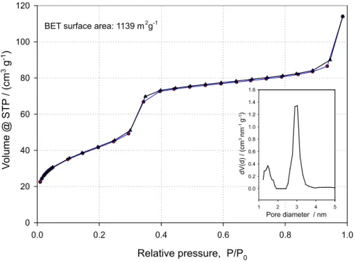
and 180 mL of water at 80 °C. After 30 min, 3.0 mL of tetraethyl orthosilicate (TEOS, Aldrich) were added dropwise under fast stirring and the resulting suspension was kept at 80 °C for 2 h. The suspension was allowed to cool to room temperature and was iltered and thoroughly washed until the pH of the iltrate was between 6.5 and 7. The material was dried overnight at 80 °C and then heated at 550 °C for 3 h to eliminate excess CTAB. This mesostructured silica shows a narrow pore size distribution with an average pore diameter of 4.6 nm, a pore volume of 0.96 cm3 g−1 and a surface area of 1139 m2 g−1.
Synthesis of CdSiO3 nanoparticles
All reagents were used as received. CdSiO3 powders
were prepared using CdCl2 (Merck) as the cadmium source
and two different sources of silicon: commercial sodium metasilicate, Na2SiO3 (Vetec) and a mesostructured silica
obtained by the surfactant-templating route described above. The reagents (1:1 Cd:Si molar ratio) were mixed and ground for 10 min in an agate mortar using small amounts of ethanol to aid in mixing. The resulting thick slurry was dried overnight at 60 °C, after which it was ground again. This dry mixture was heated at 580 °C for 60 min using a 5 °C min-1 ramp, and was allowed to cool
overnight inside the oven. One experiment using CdCl2
and Na2SiO3 was also done at 570 °C. The resulting
CdSiO3 powders were thoroughly washed in deionized
water until no Cd2+ could be detected by addition of
S2−(aq) to the iltrate and no Cl− could be detected by
addition of Ag+(aq). For clarity, the material prepared
using sodium silicate will be called SS-CdSiO3 and the
material prepared using mesostructured silica will be called MS-CdSiO3.
The CdSiO3 nanostructures and the mesostructured
SiO2 precursor were characterized by X-ray diffraction
(XRD, Shimadzu Maxima XRD-7000, CuKα, 15.418 nm, 2°per min), scanning electron microscopy (SEM, JEOL JSM-7401 FESEM, operating in SEI mode at 5 kV), transmission electron microscopy (TEM, Zeiss CTEM 902, operating at 80 kV), and focused ion beam microscopy (FIB, FEI Nova 200 Dual Beam SEM/FIB, 5 kV). The BET surface areas given as Supplementary Information (Figure S2) were determined by nitrogen adsorption (Quantachrome Nova 1000e Surface Area Analyzer).
Results and Discussion
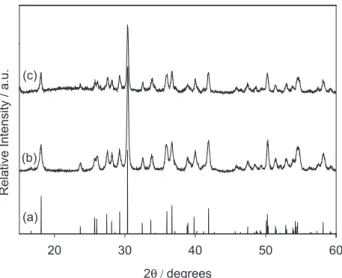
Figure 1 shows the XRD patterns of CdSiO3 (JCPDS
A comparison of the diffractograms with JCPDS Card No. 35-0810 (Figure 1a) conirms that SS-CdSiO3 consists
of pure, single-phase CdSiO3, whose structure is expected
to be similar to that of pseudowollastonite, CaSiO3.10 We
can also see that MS-CdSiO3 is slightly less crystalline
and exhibits a halo between 2θ = 20 and 30°. Sodium metasilicate is sometimes also described as Na2O•SiO2,
and sodium oxide can react with silica to form the silicate structure which, in the presence of molten CdCl2, forms
the desired product. The attack of SiO2 by Na2O prior to
CdSiO3 formation probably leads to higher crystallinity.
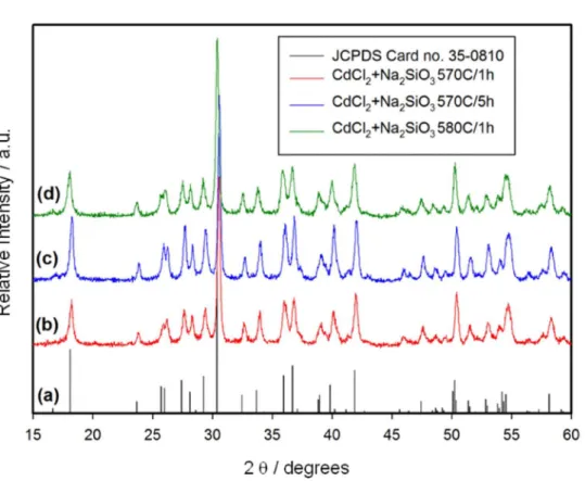
The XRD patterns of the materials obtained from CdCl2
and Na2SiO at 570 °C for 1 and 5 h (Figure S1) are almost
identical to that obtained at 580 °C for 1 h, but are shifted by 0.15° to higher values of 2θ (for example, the strongest peak occurs at 2θ = 30.40° and 30.55° for the samples heated at 580 and 570 °C respectively). This indicates that, although the material forms at 570 °C, that is, soon after the melting of CdCl2, the ordering of the structure is not
complete below 580 °C.
The use of a high surface area mesostructured silica also yields CdSiO3, although with a somewhat lower crystallinity,
as evidenced by the broader, less intense XRD peaks. The broad halo between 2θ = 20 and 30° indicates that the reaction is not complete, and some amorphous SiO2 remains.
However, low-angle X-ray diffraction (Figure 2) shows that the mesostructure of silica is lost upon the partial conversion to CdSiO3. At the reaction temperature, we expect SiO2 to
be less reactive than the Na2O present in the metasilicate
precursor. In this case the precursor surface area does play a fundamental role, allowing a more effective contact between the molten CdCl2 and the Si source. When we used
commercial fused silica with a lower surface area (354 m2 g-1)
as the Si source, no CdSiO3 was formed at 580 °C for 1 h.
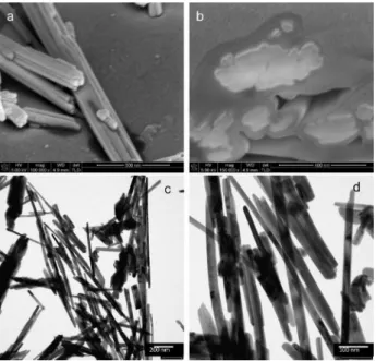
The SEM results are shown in Figure 3. The images show that there is a signiicant inluence of the Si source on the morphology of the resulting product which, in
Figure 1. XRD patterns for (a) JCPDS Card No. 35-0810; b) SS-CdSiO3; c) MS-CdSiO3.
Figure 2. Low angle X-ray diffractograms of MS-CdSiO3 (a) and of the
mesostructured silica used in this work (b). For comparison, the JCPDS card for MCM-41 silica is also shown (c).
both cases, is very different from the large aggregates seen when the conventional solid state route is used. The material SS-CdSiO3 (Figure 2 a-c) is composed
of needle-shaped nanoparticles which relect the low dimensionality of the crystal structure. The individual needles are 1-4 µm long by 50-100 nm wide and can be arranged in bundles forming long wires with diameters in the micrometer range, as shown in Figure 2c. This type of morphology cannot be observed in CdSiO3 prepared
by the conventional high-temperature solid state reaction because the high temperatures and long heating times favor particle coalescence into irregular agglomerates. In contrast, the material MS-CdSiO3 (Figure 3 d-f) shows
a coralloid morphology with approximate diameters around 100 nm. The coralloid shape is an indication that CdSiO3 forms initially in the spherical shape of the
precursor silica particles (Figure S3). This means that molten CdCl2 diffuses into the mesostructures, covering
their surface and reacting to form CdSiO3. The presence
of elongated structures in Figure 3f suggests that heating at higher temperatures may lead to the formation of the elongated structures seen in SS-CdSiO3. This morphology
control may have important implications when using these materials as a matrix for long lasting phosphorescence, especially for medical applications, where the shape and size of the particles may determine their path through the human body. To check if these needle-shaped particles are nanotubes, which should be hollow, SS-CdSiO3
was observed by FIB microscopy and TEM as shown in Figure 4. The FIB images (Figure 4 a-b) show that the individual nanoparticles have an approximately circular cross-section, diameters as small as 25 nm,
and are not hollow, which means that they are best described as nanorods. Transmission electron microscopy (Figure 4 c-d) shows that the primary nanoparticles are 500-700 nm long by 20-50 nm wide, with high aspect ratios, varying from 10:1 to 35:1.
Conclusions
CdSiO3 nanostructures have been prepared at the lowest
temperature and shortest reaction times known to us, using two very simple synthetic routes. The use of molten CdCl2 as a reagent in a molten salt-type approach yields
pure, single-phase nanorods when Na2SiO3 is used as the
Si source, while a coralloid morphology, representing a transition from spherical to needle-like form, is observed when the Si source is high surface area mesostructured SiO2. In this case, the conversion is not complete and
amorphous silica is still present. This is a very promising method because it is simple, straightforward and cost-effective. The choice of an adequate precursor allows a morphology control of the resulting particles, with possible implications in medical applications.
Supplementary Information
Supplementary data are available free of charge at http://jbcs.sbq.org.br as PDF ile.
Acknowledgments
We would like to acknowledge the Centro de Componentes Semicondutores (CCS) at the University of Campinas (UNICAMP), especially Prof. Oswaldo Luiz Alves and Alfredo Rodrigues Vaz for the FIB images, and Dr. Carlos Alberto de Paula Leite and Prof. Fernando Galembeck (UNICAMP) for the TEM images. This work is funded in part by the Conselho Nacional de Desenvolvimento Cientíico e Tecnológico (CNPq), Brazil, and by the Fundação de Amparo à Pesquisa do Estado de São Paulo (FAPESP), Brazil.
References
1. Chang, C. K.; Mao, D. L.; Shen, J. F.; Feng, C. I.; J. Alloys Compd. 2003, 348, 224.
2. Lin, L.; Shi, C. S.; Wang, Z. F.; Zhang, W. P.; Yin, M.; J. Alloys Compd. 2008, 466, 546.
3. Lin, L.; Yin, M.; Shi, C. S.; W. Zhang, W. P.; J. Alloys Compd.
2008, 455, 327.
4. Gary, E. N.; A History of Luminescence; American Philosophical Society: Philadelphia, PA, 1957, p. 18.
5. Gubelin, E.; International World of Gemstones; ABC-Verlag: Zurich, 1974.
6. Feldman, C.; Justel, T.; Ronda, C. R.; Schmidt, P. J.; Adv. Funct. Mater.2003, 13, 511.
7. Green, W. H.; Lee, K. P.; Grey, J.; Au, T. T.; Sailor, M. J.; Science 1997, 276, 1826.
8. Wang, X.; Zhuang, J.; Chen, J.; Zhou, K. B.; Li, Y. D.; Angew. Chem., Int. Ed. 2004, 43, 2017.
9. Wang, X.; Zhuang, J.; Peng, Q.; Li, D.; J. Solid State Chem. 2005, 178, 2332.
10. Ferracin, L. C.; Davolos, M. R.; Nunes, L. A. O.; J. Lumin. 1997,72-74, 185.
11. Dent, L. S.; Glasser, F. P.; Inorg. Chem.1964, 3, 1228. 12. Barboza, C. A.; Henriques, J. M.; Albuquerque, E. L.; Caetano,
E. W. S.; Freire, V. N.; da Costa, L. A. O.; Chem. Phys. Lett. 2009, 480, 273.
13. Zhang, L.; Hong, G. Y.; Sun, X. I.; Chin. Chem. Lett.1999, 10, 799.
14. Lei, B.; Liu, Y.; Ye, Z.; Shi, C.; Chem. Lett.2003, 32, 904. 15. Lei, B.; Liu, Y.; Ye, Z.; Shi, C.; J. Solid State Chem.2004, 177,
1333.
16. Kuang, J.; Liu, Y.; Chem. Phys. Lett. 2006, 424, 58. 17. Liu, Y.; Lei, B.; Shi, C.; Chem. Mater.2005, 17, 2108. 18. Liu, Y.; Kuang, J.; Lei, B.; Shi, C.; J. Mater. Chem. 2005, 15,
4025.
19. Lei, B.; Liu, Y.; Ye, Z.; Shi, C.; J. Lumin.2004, 109, 215. 20. Parhi, P.; Manivannan, V.; Mater. Lett.2008, 62, 3468. 21. Qu, X.; Cao, L.; Liu, W.; Su, G.; Qu, H.; Xu, C.; J. Alloys
Compd. 2009, 484, 641.
22. Wang, J.; Ge, J.; Zhang, H.; Li, Y.; Small2006, 2, 257. 23. Mao, Y.; Park, T. -J.; Zhang, F.; Zhou, H.; Wong, S. S.; Small
2007, 3, 1122.
24. Hayashi, Y.; Kimura, T.; Yamaguchi, T.; J. Mater. Sci.1986, 21, 757.
25. Yoon, K. H.; Cho, Y. S.; Kang, D. H.; J. Mater. Sci.1998, 33, 2977.
Submitted: January 25, 2011
Published online: August 9, 2011
Supplementary Information
S
I
J. Braz. Chem. Soc., Vol. 22, No. 10, S1-S2, 2011. Printed in Brazil - ©2011 Sociedade Brasileira de Química 0103 - 5053 $6.00+0.00
*e-mail: [email protected]
Low Temperature Synthesis of CdSiO
3Nanostructures
Leonardo P. Santana, Erick S. de Almeida, Jones L. Soares and Flavio M. Vichi*
Instituto de Química, Universidade de São Paulo, Av. Prof. Lineu Prestes, 748, Bloco 3T, Sala 325, 05508-900 São Paulo-SP, Brazil
Figure S1. X-ray diffractograms. (a) JCPDS Card 35-0810 (CdSiO3); (b) material resulting from heating stoichiometric amounts of CdCl2 and Na2SiO3
at 570 °C for 1 h; (c) material resulting from heating stoichiometric amounts of CdCl2 and Na2SiO3 at 570 °C for 5 h; (d) material resulting from heating
Figure S2. Nitrogen adsorption / desorption isotherm and BJH pore size distribution (inset) for the mesostructured silica used in this work.