The Double Gaussian Distribution of Inhomogeneous Barrier Heights in Al/GaN/p-GaAs (MIS)
Schottky Diodes in Wide Temperature Range
S. Zeyrek1∗, M. M. B¨ulb¨ul2, S¸. Altındal2, M. C. Baykul3, and H. Y¨uzer4
1Department of Physics, Faculty of Arts and Sciences, Dumlupınar University, 43100, K ¨utahya-Turkey 2Department of Physics, Faculty of Arts and Sciences, Gazi University, 06500, Ankara–Turkey
3Department of Physics, Osmangazi University, 26480, Eskis¸ehir-Turkey 4Material and Chemical Technologies Research Institute,
Marmara Research Center, P.O. Box 21, 41470 Gebze-Kocaeli, Turkey
(Received on 18 September, 2008)
The current-voltage (I-V) characteristics of metal-insulator-semiconductor (Al/GaN/p-GaAs) Schottky bar-rier diodes (SBDs) were investigated over a wide temperature range of 80-380 K. By using the thermionic emission (TE) theory, the zero bias barrier heightΦB0calculated from I-V characteristics was found to increase with increasing temperature as the ideality factor n decreases with increasing temperature, and especially the activation energy plot is nonlinear at low temperatures. The observed variation in theΦB0and n is attributed to the spatial barrier inhomogeneities in SBD by assuming a Gaussian distribution (GD) of barrier heights (BHs). The experimental I-V-T characteristics of the SBDs have shown a double Gaussian distribution having mean barrier heights ¯ΦBof 0.854 eV and 0.395 eV and standard deviationsσsfor 0.142 V and 0.059 V, respectively. The modified ln(Io/T2)-q2σo2/2(kT)2vs q/kT plot givesΦB0and Richardson constant A∗as 0.858 eV and 0.364 eV, and 78.5 and 128 A/cm2K2, respectively, without using the temperature coefficient of the barrier height. Hence, the results have shown that the I-V-T characteristics of the Al/GaN/p-GaAs SBDs can be successfully explained on the basis of TE mechanism with a double Gaussian distribution of the barrier heights.
Keywords: MIS diode; Barrier inhomogeneities; Double Gaussian distribution; Temperature; Dependence; Nitride passivation
1. INTRODUCTION
Metal-semiconductor (MS) and metal-insulator-semiconductor (MIS) Schottky barrier diodes (SBDs) play a very important role in the micro electronic devices. These type devices have important application in a wide vari-ety of the optoelectronic, bipolar integrated circuits and high frequency applications. There are currently a vast number of experimental studies on diode characteristics parameters such as Schottky barrier heights (SBHs), ideality factor n, series resistance Rs and surface states Nssin a great variety of MS and MIS type SBDs [1-17]. The performance and reliability of these devices especially depends on formation of insulator layer between metal and semiconductor interface, the density of interface states distribution between semiconductor and insulator layer, series resistance and inhomogeneties of Schottky barrier contacts.
The characterization of a SBD with an interface layer does not obey the ideal Schottky theory. Especially understanding Schottky barrier formation between metal and semiconductor interface on a fundamental basis still remains a challenging problem. Also, Schottky barrier height, and ideality factor are the fundamental parameters of the MS or MIS structures and strongly effected devices performance.
Also, in a broad temperature range or at room tempera-ture current-voltage (I-V) measurements alone do not pro-vide detailed information about the nature of barrier forma-tion between metal and semiconductor and current-transport mechanisms. The analysis of the I-V characteristics of MS or MIS SBDs at wide temperature range allows us to understand
∗E-mail address: [email protected]
different aspects of barrier formation and current-transport mechanisms [9,15-18]. In general, the I-V-T characteristics of SBDs based on Thermionic Emission (TE) usually reveal an abnormal increase in the SBH and a decrease in the ideal-ity factor n with decrease in temperature [9,18-20]. In addi-tion, the decrease in the BH at low temperatures leads to non-linearity in the activation energy plot ln (Io/T2)vs 1/T plot. This abnormal behaviour of SB at low temperature has been attributed to be the spatial variation of BHs in the Al/GaN/p-GaAs (MIS) Schottky diodes. Recently, the spatial barrier ho-mogeneities in MS and MIS type SBDs are described mainly by a Gaussian distribution function and is widely used to ex-plain the experimental I-V characteristics [11,16, 20,22,23].
Gallium arsenide is one of the advantageous semiconduc-tors for high-speed and low-power devices [1]. The formation of a direct on GaAs by traditional ways oxidation or depo-sition cannot completely passivate the active dangling bonds at the semiconductor surface. Thus, various non-traditional approaches for surface passivation sulfide, selenide layer and nitride formation have been a subject of increasing interest in recent years [37-48,50].
As known, there are many techniques for nitridation process. Electrochemical anodization technique is an economical and practical way to produces a very thin film on the GaAs sub-strate [17,37-40,50]. We used same technique in our previous work, too [17].
We present, in this work, non-aqueous ammonium polyni-tride ((NH4)2(NH2)x) electrolyte was employed to grow a Gallium nitride layer on the GaAs surface as a new method of nitride passivation. Nitridation of GaAs surface was also performed by electrochemical anodization technique. The I-V characteristics of Al/GaN/p-GaAs SBDs were investigated over a wide temperature range of 80-380 K. The tempera-ture dependence of barrier height (SBHs) characteristics of Al/GaN/p-GaAs (MIS) diodes were interpreted on the basis of the existence of Gaussian distribution of the BHs around a mean value due to barrier height inhomogeneities prevailing at the metal-semiconductor interface.
2. EXPERIMENTAL PROCEDURE
Al/GaN/p-GaAs (MIS) Schottky barrier diodes were fabri-cated on 2 inch diameter float zone (100) p-type (Zn doped) single crystal GaAs wafer having thickness of 280µm. The sample was ultrasonically cleaned in trichloroethylene and ethanol, etched by H2SO4/H2O2/H2O=5:1:1 (weight ratio) so-lution for 30 s., rinsed by propylene glycol and blown with dry nitrogen gas. The back contacts of the electrodes were formed by evaporating Al in high vacuum (P=10−6 Pa) and subse-quently to form ohmic contact annealing them for a few min-utes at 450oC. After making of electrical contact, the walls and under side of the GaAs wafer were insulated with the high-quality wax. The nitridation set-up, using in the study is the electrochemical anodization cell which consists of a p-GaAs anode and Pt cathode. An agitation of the electrolyte is achieved by magnetic stirrer. Electrolyte used in the experi-ment was obtained by sequentially mixing of propylene gly-col with ammonia (NH3)and hydrazine (NH2-NH2)at 21:3:1 weight ratio, respectively. Preceding each of cleaning step, the wafer was rinsed thoroughly in de-ionized water with re-sistivity of 18 MΩcm.
Immediately after that, the substrate was immersed in elec-trolytical cell. Anodic nitridation was performed using a con-stant current source at different current densities, under light and N2flow, at room temperature (293 K). The potential dif-ference between the electrodes normalized to calomel elec-trode was measured with an x-t recorder. The anodization was stopped, when the cell voltage reached about the 25 V. After, the sample was immediately rinsed in propyl alcohol and blown dry nitrogen and left in a desiccators. The Schottky contacts were formed by evaporating of Al dots with diameter of about 1.0 mm and 2500 ˚A thick in high vacuum (P=10−6 Pa). The metal thickness of layer and the deposition rates were monitored with the help of quartz crystal thickness monitor. In this way, metal-interfacial insulator layer-semiconductor (Al/GaN/p-GaAs) MIS Schottky barrier diodes were fabri-cated on p-type GaAs wafer. The interfacial insulator layer thickness (GaN) was estimated to be about 63 ˚A from
mea-surement of the insulator capacitance in the strong accumula-tion.
The current-voltage (I–V) measurements were performed by the use of a Keithley 220 programmable constant cur-rent source, a Keithley 614 electrometer. I-V characteristics were measured in the temperature range of 80-380 K using a temperature controlled Janes vpf-475 cryostat, which en-ables us to make measurements in the temperature range of 77-450 K. The interfacial layer thickness was estimated to be about 63 ˚A from the oxide capacitance measurement in the strong accumulation region at high frequency (1MHz). The sample temperature was always monitored by using a copper-constantan thermocouple close to the sample and measuring with a dmm/scanner Keithley model 199 and a Lake Shore model 321 auto-tuning temperature controllers with sensitiv-ity better than±0.1 K. All measurements were carried out with the help of a microcomputer through an IEEE-488 ac/dc converter card.
3. RESULTS AND DISCUSSIONS
3.1. Temperature dependence of the forward bias I-V characteristics
The current-voltage (I-V) measurements of the Al/GaN/p-GaAs (MIS) Schottky diodes were performed in the temper-ature range of 80-380 K . For a MIS Schottky diode, it is as-sumed that the current of the device is due to TE theory and it can be expressed as [1,2]
I=Ioexp
µqV nkT
¶ · 1−exp
µ −qVkT
¶¸
(1)
where Iois the reverse saturation current derived from the for-ward bias semi-logarithmic lnI-V plots and expressed as
Io=A A∗T2exp
µ −qΦkTB0
(2)
where q is the electronic charge,A∗is the effective Richardson constant and equals 74.4 A cm−2K−2for p-type GaAs [25],A is the effective diode area, k is the Boltzmann constant, T is the temperature in K,ΦBo(I-V) is the zero bias barrier height andn is the ideality factor. The ideality factor is calculated from the slop of the linear region of the forward bias ln(I)-V plots and can be written from Eq.(1) as
n= q kT
µ dV
d(lnI) 
(3)
The zero-bias barrier heightΦB0(=ΦB(I-V)) is determined from the extrapolated Ioand is given by
ΦB0= kT
q ln
·AA∗T2 I0
¸
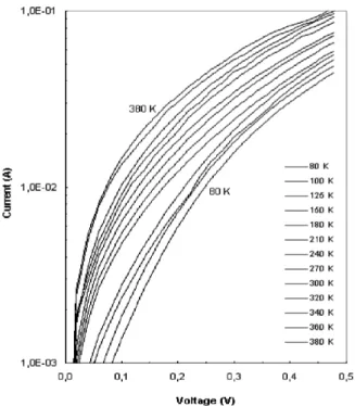
FIG. 1: Experimental forward bias current-voltage (I-V) character-istics of the Al/GaN/p-GaAs (100) Schottky MIS diode at various temperatures.
The forward bias semi-logarithmic lnI-V characteristics for Al/GaN/p-GaAs Schottky diode in the temperature ranging from 80 K to 380 K are shown in Fig. 1. The I-V plots shift towards the higher bias side with decreasing tempera-ture. The experimental values of the barrier heightΦB0and the ideality factor n for the devices were determined from in-tercepts and slopes of the forward-bias ln(I) versus V plot at each temperature, respectively. The values of n andΦBowere calculated from Eq.(3) and (4), respectively, at each tempera-ture and shown in Table 1and Figs. 2 and 3, respectively. As shown in Table 1, the experimental values ofΦB0and n for the Al/GaN/p-GaAs (100) Schottky diodes ranged from 0.562 eV and 1.64 (at 380 K) to 0.115 eV and 8.16 (at 80 K), respec-tively. The Al/GaN/p-GaAs Schottky diode with the ideal-ity factor value of 2.39 at 300K obey a metal-insulator layer-semiconductor (MIS) structure. This ideality factor value is significantly larger than an ideality Schottky diode. Such be-havior of ideality factor has been attributed to particular dis-tribution of interface states and insulator layer between metal and semiconductor [4,15]. This indicates that formed of an insulator layer (GaN) on the p-GaAs surface. Also, the val-ues of ideality factor n was found to increase, while theΦB0 decrease with decreasing temperature, as can be seen Figs. 2 and 3, respectively.
As explained in refs.[11,17,26-30], since the current trans-port across the metal-semiconductor (MS) interface is a temperature-activated process; electrons at low temperatures are able to surmount the lower barriers. Therefore, the current transport will be dominated by the current flowing through the
FIG. 2: Temperature dependency of the ideality factor for Al/GaN/p-GaAs (100) Schottky MIS diodes.
FIG. 3: Temperature dependency ofΦB0 (I-V) obtained from I-V characteristics for Al/GaN/p-GaAs (100) Schottky MIS diodes.
patches of lower Schottky barrier height (SBH), leading to a larger ideality factor. In other words, more and more electrons have sufficient energy to overcome the higher barrier build up with increasing temperature and bias voltage. An apparent in-crease in the ideality factor and a dein-crease in the barrier height at low temperatures are caused possibly by other effects such as non-uniformity of thickness and the interfacial charges.
3.2. Barrier heights inhomogeneities
TABLE I: Temperature dependent values of various parameters determined from I-V characteristics of Al/GaN/p-GaAs(100) Schottky MIS diodes in the temperature range of 80-380 K.
T(K) 80 100 125 150 180 210 240 270 300 320 340 360 380
n 8.16 6.67 5.69 4.55 4.15 3.52 3.06 2.73 2.39 2.35 2.32 2.10 1.64
ΦB0 0.115 0.145 0.182 0.221 0.261 0.308 0.354 0.401 0.444 0.475 0.504 0.532 0.562
while the ΦB0 decreases with decreasing temperature [20] and this behaviour lead to nonlinearity in the activation en-ergy plot. Here, we show the conventional enen-ergy variation of ln(Io/T2) versus 1/T for Al/GaN/p-GaAs metal-insulator-semiconductor MIS Schottky barrier diodes. According to Eq.(2), one obtains
ln µI
0 T2
¶ =ln¡
AA∗T2¢−qΦBo
kT (5)
The temperature dependency of experimental ln(Io/T2) ver-sus 1/T plot was found to be non-linear in the tempera-ture range measured (not shown here). The deviation in the Richardson plots may be due to the spatial inhomo-geneities of the barrier height and potential fluctuations at the interface that consist of low and high barrier areas [9-12,16,18,20,26,33-35]. That is, the carrier transport mecha-nism across MS contact would flow preferentially through the lower barriers in the potential distribution [9-12,16,18,20,33-35]. As was explained by Horvath [28], the A∗value obtained from the temperature dependency of the I-V characteristics may be affected by the lateral inhomogeneity of the barrier.
The commonly observed deviation of classical thermionic emission theory can be explained by a recent model based on the assumption of a spatial fluctuation of the BH at in-terface. Namely, depending on temperature, the observed changes may be interpreted satisfactorily by incorporation of the concept of barrier inhomogeneities into thermionic emis-sion theory [30]. In a real Schottky diode, the barrier height may not be the same over the entire area of contact due a varia-tion in the thickness and/or composivaria-tion of the interfacial layer and non-uniformity of the interfacial charges, etc [22,33].The barrier inhomogeneity approach mainly assumes that there is a distribution of barrier heights over the rectifying contact. Various types of distribution functions are suggested for de-scribing barrier height inhomogeneities, for example Gaus-sian [16,22,23] and log-normal [49].
In order to explain the abnormal behavior between the the-oretical and experimental values of Richardson constant A*, let us assume a barrier height with a mean value ¯ΦB0and stan-dard deviationσs, which can be given as [1,10-12,15,17,18].
P(ΦB) = 1
σs √
2πexp
·
−(ΦB−Φ¯B) 2
2σ2
s
¸
(6)
where 1/σS √
2π is the normalization constant of the Gaus-sian barrier height distribution. Under forward bias, the total current I(V) across a Schottky diode containing barrier inho-mogeneities can be expressed as
I(V) =
Z +∞
−∞
I(ΦB,V)P(ΦB)dΦ (7) where I(ΦB,V) is the current at a bias V for a barrier height based on the ideal thermionic-emission-diffusion (TED) the-ory and P(ΦB)is the normalized distribution function giving the probability of accuracy for barrier height.
Now, introducing I(ΦB,V) and P(ΦB)from Eq.(1) and (6) into Eq.(7), and performing integration from -∞to +∞, one can obtain the current I(V) through a Schottky barrier at a for-ward bias V, similar to Eq.(1) and (2) but with the modified barrier
I(V) =AA∗T2exp ·
−kTq µ
−
ΦB−
qσ2S
2kT ¶¸
exp µ
qV napkT
¶ · 1−exp
µ −qVkT
¶¸
(8)
with
Io=A A∗T2 exp
µ −qΦkTap
(9)
whereΦapand napare the apparent barrier height and appar-ent ideality factor, respectivelyΦapis given by [14,18],
Φap=Φ¯B0(T=0) − qσ2s
2kT (10)
The temperature dependency ofσsis usually small and can be neglected [33]. In addition, the observed variation of the apparent ideality factor n with temperature T in the model is given by [16].
µ 1 nap−
1 
=ρ2− qρ3
2kT (11)
It is assumed that the mean SBH, ¯ΦB, and σs are linearly bias dependent on Gaussian parameters, such as ¯ΦB=Φ¯B0+
low temperatures. Fitting of the experimental data in Eq.(2) or (9) and in Eq.(3) gives Φap andnap, respectively, which should obey Eq. (10) and (11).
The continuous curves in Figs. 2 and 3 and the linearity of the apparent barrier height and ideality factor versus q/2kT curves in Figs. 4 and 5 show that the temperature depen-dence experimental data of Al/GaN/p-GaAs (100) Schottky contact are in agreement with the recent model which is re-lated to thermionic emission over a Gaussian BH distribution. Thus, the plot ofΦapversus q/2kT (Fig. 5) is expected to be a straight line with the intercept at the ordinate determining the zero-bias mean BH ¯ΦB0and the slope giving the zero-bias standard deviation σs. The experimental Φap versus q/2kT andnap versus q/2kT plots (Figs. 4 and 5) drawn using the data obtained from Fig. 1 respond to two lines instead of a sin-gle straight line with transition occurring at 180 K. These two different slopes at the lower and higher temperatures indicate two activated process with different mean barrier heights. The above observations show the existence of two Gaussian distri-butions of barrier heights in the contact area. Two sets of val-ues of ¯ΦB0andσsare obtained from the intercepts and slopes of these straight lines as 0.854 eV and 0.142 V in the tem-perature range of 210-380 K (distribution 1), and as 0.395 eV and 0.059 V in the temperature range 80-180 K (distribution 2). Moreover, the values ofΦapestimated from equation (4) over the entire temperature range curves 1 and 2 can be seen in Fig. 3. The existence of a double Gaussian in the metal-semiconductor (MS) contacts can be attributed to the nature of their inhomogeneities in the two cases. This may involve variation in the interface composition/phase, interface qual-ity, electrical charges, nonstoichiometry, etc.. They electri-cally influence the I-V characteristics of the Schottky diodes, at particularly low temperatures. Hence, I-V measurements at very low temperatures can show the nature of barrier inhomo-geneties existing in the contact area. That is, the presence of a second Gaussian distribution at very low temperatures may possibly occur due to some phase change taking place on cool-ing below a certain temperature. Furthermore, the temperature range covered by each straight line suggests the regime where the corresponding distribution is effective [30,33].
The above results have shown that the I-V-T characteristics of the Al/GaN/p-GaAs SBDs can be successfully explained on the basis of TE mechanism with a double Gaussian distri-bution of the barrier heights.
The plot ofnapvs q/2kTshould be a straight line that gives voltage coefficientsρ2andρ3from the intercept and slope, re-spectively (Fig. 5). The values ofρ2obtained from the inter-cepts of the experimentalnapvs q/2kTplot (Fig. 5) are -0.154 V in 210-380 K range (distribution 1) and -0.643 V in 80-180 K range (distribution 2), whereas the values ofρ3 from the slopes are - 0.0213 V in 210 - 380 K range and - 0,0034 V in 80 - 180 K range. The linear behavior of this plot demon-strates that the ideality factor does indeed express the voltage deformation of the Gaussian distribution of the Schottky BH. According to these results, this inhomogeneity and potential fluctuation dramatically affect low temperature I-V character-istics.
The computed values exactly coincide with the
experimen-FIG. 4: The zero-bias apparent barrier height (ΦB0 (I-V)) versus q/2kT plot for Al/GaN/p-GaAs(100) Schottky MIS diode according to double Gaussian distribution.
tal results in the respective temperature ranges for two differ-ent distributions. As can be seen from thenapvs q/2kT plot, ρ3value or the slope of the distribution 1 is larger than that of distribution 2. Therefore, the distribution 2 at very low tem-peratures may possibly take place due to some phase change on cooling below a certain temperature.
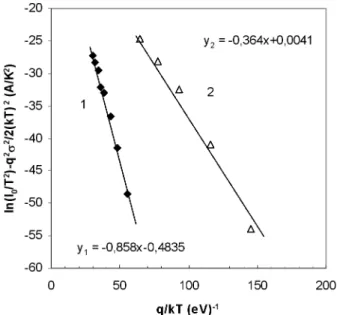
FIG. 6: Temperature dependence of ln(Io/T2)-q2σ02/2(kT)2) versus
q/kT for Al/GaN/p-GaAs (100) Schottky MIS diodes.
The conventional Richardson plot is now modified by com-bining Eqs. (10) with (11) as follows
ln µ
I0 T2
¶ −
µ q2σ2o 2k2T2
=ln(AA∗)− qΦkT¯B0 (12)
The plot of a modified ln(I0/T 2) - q2σ2o/2k2T 2 vs q/kT according to Eq.(12) should give a straight line with the slope directly yielding the mean ¯ΦB0and the intercept (=lnAA*) at the ordinate determining A* for a given diode area A. Fig. 6 shows this plot.
The ln(Io/T 2) - q2σ2o/2k2T 2 values were calculated for both values ofσo obtained for the temperature range of 80-180 K and 210-380 K. The open triangles and closed squares in Fig. 6 have given the modified ln(I0/T 2) - q2σ2o/2k2T 2 vs q/kT plots for both values of σoand zero-bias mean BH
¯
ΦB0 obtained 0.364 eV in 80-180 K range ( distribution 2)
and 0,858 eV in 210-380 K range (distribution 1). These val-ues match exactly with the mean BHs obtained from theΦap versus q/2kT plots in Fig. 6. The intercepts at the ordinate give the Richardson constant A* as 128 A/cm2K2in 80-180 K range and 78.5 in 210-380 K range without using the temper-ature coefficient of the BHs. The Richardson constant value of 78,5 A/cm2K2 for the range of 210-380 K is almost the same as the value of 74.4 A/cm2K2known for holes in p-type GaAs. As can be seen, the values of ¯ΦB00.858 eV and 0.364 eV from this plot is in close agreement with the values of ¯ΦB0 0.854 eV and 0.395 eV from the plot ofΦapversus q/2kT.
4. CONCLUSION
Current-voltage (I-V) characteristics of Al/GaN/p-GaAs SBDs were measured in the temperature range of 80-380 K. The results underline the importance of investigations in a wide temperature range since I-V measurements at room tem-perature alone do not provide satisfactory insights. The ex-perimental results have showed the non-ideal behavior of the current-transport over the barrier expressed by ideality factors, significantly larger than unity at lower temperatures and an in-creasingly effective SBH with rising temperature. The high value ofnis attributed to the potential drop in the interfacial insulator layer and recombination through the interface states. In order to obtain evidence of single or double/multiple Gaus-sian distribution of the BHs, we have drawn Φap vs q/2kT plot. We obtained two straight lines with negative slope for double Gaussian distribution of BHs. While the slope of each straight line gives the standard deviation, the intercept at the ordinate yields the mean of the Gaussian distribution. Then, the values of Richardson constant A∗ were obtained from a modified ln(Io/T2)-q2σ2o/2(kT)2vs q/kT plot as 128 A/cm2K2 in 80-180 K and 78.5 A/cm2K2 in 210-380 K. It has been concluded that the I-V-T characteristics of Al/GaN/p-GaAs SBDs can be satisfactorily explained on the bases of TE mech-anism with two Gaussian distributions of the Schottky barrier heights in the temperature range of 80-380 K. In this study has not been described in detail of properties of nitridation layer (GaN). However, in this study indicates existence of an insulator layer (GaN) because the behavior of ideality factor and double Gaussian distribution of barrier height has been attributed insulator layer between metal and semiconductor.
5. ACKNOWLEDGEMENT
This work is partly supported by Turkish of Prime Ministry State Planning Organization Project Number 2001K120590.
[1] S. M. Sze,Physics of Semiconductor Devices, 2nd Edn. Willey, New York 1981, p.850.
[2] E. H. Rhoderick, R. H. Williams, Metal-Semiconductor Con-tacts,2nd Ed. Clarendon Press, Oxford, 1988.
[3] C. R. Crowell and S. M. Sze, J. Appl. Phys.36, 3212 (1965). [4] H. C. Card, E. H. Rhoderick, J. Phys. D: Appl. Phys.4, 1589
(1971).
68(7), 3475 (1990).
[6] P. Cahttopadhyay, A. N. Daw, Solid-State Electron. 29, 555 (1986).
[7] P. Cova and A. Singh, Solid-State Electron.33, 11 (1990). [8] M. O. Aboelfotoh, J. Appl. Phys.69, 3351 (1991).
[9] S¸. Karatas¸, S¸. Altındal, A. T¨ur¨ut, and A. ¨Ozmen, Appl. Surf. Sci.217, 250 (2003).
[10] M. K. Hudait, P. Venkateswarlu, and S. B. Krupanidhi, Solid-State Electron.45, 133 (2001).
[11] S. Chand, Semicond. Sci. Technol.19, 82 (2004).
[12] S. Zhu, R. L. Van Meirhaeghe, C. Detavernier, G. P. Ru, B. Z. Li, and F. Cardon, Solid-State Comm.112, 611 (1999). [13] J. P. Sullivan, R. T. Tung, M. R. Pinto, and W. R. Graham, J.
Appl. Phys.70, 7403 (1991).
[14] B. Akkal, Z. Benemara, A. Boudissa, N. B. Bouiadjra, M. Am-rani, L. Bideux, and B. Gruzza, Mater. Sci. And Eng. B,55, 162 (1998).
[15] S¸. Altındal, S. Karadeniz, N. Tuˇgluoˇglu, and A. Tataroˇglu, Solid-State Electron.47, 1847 (2003).
[16] J. H. Werner and H. H. G¨uttler, J. Appl. Phys.69, 1522 (1991). [17] S. Zeyrek, S¸. Altındal, H. Y¨uzer, and M. M. B¨ulb¨ul, Appl. Surf.
Sci.252, 2999 (2006).
[18] S. Zhu, R. L. Van Meirhaeghe, C. Detavernier, F. Cardon, G. P. Ru, X. P. Qu, and B. Z. Li, Solid-State Elecron.44, 663 (2000). [19] S. Hardikar, M. K. Hudait, P. Modak, S. B. Krupanidhi, and N.
Padha, Appl. Phys. A68, 49 (1999).
[20] A. G¨um¨us¸, A. T¨ur¨ut, and N. Yalc¸ın, J. Appl. Phys.91, 245 (2002).
[21] K. Yasui, T. Arayama, S. Okutani, and T. Akahane, Appl. Surf. Sci.212-213, 619 (2003).
[22] Y. P. Song, R. L. Van Meirhaeghe, W. H. Laflere, and F. Cardon, Solid-State Electron.29, 633 (1986).
[23] P. G. McCafferth, A. Sellai, P. Dawson, and H. Elabd, Solid-State Electron.39, 583 (1996).
[24] V. L. Berkovits, T. V. L’vova, and V. P. Ulin, Vacuum57, 201 (2000).
[25] E. H¨okelek, Y. Robinson, Solid-State Electron.24, 99 (1981). [26] S¸. Karatas¸, S¸. Altındal, and M. C¸ akar, Physica B357, 386
(2005).
[27] A. T¨ur¨ut, N. Yalc¸ın, and M. Saˇglam, Solid-State Electron.35, 835 (1992).
[28] Zs. J. Horvarth, Solid-State Electron.39, 176 (1996).
[29] F. A. Padovani, R. Stratton, Solid-State Electron.9, 695 (1966). [30] A. F. ¨Ozdemir, A. T¨ur¨ut, A. K¨okc¸e, Semicond. Sci. Technol.
21, 298 (2006).
[31] A. S. Bhuiyan, A. Martinez, and D. Esteve, Thin Solid Films
161, 93 (1988).
[32] S¸. Karatas¸ and A. T¨ur¨ut, Physica B381, 199 (2006).
[33] S. Chand and J. Kumar, Semicond. Sci. Technol. 11, 1203 (1996).
[34] S. Chand and J. Kumar, Appl. Phys. A.65, 497 (1997). [35] K. Maeda, Surf. Sci.493, 644 (2001).
[36] S. Zhu, C. Detavernier, R. L. Van Meirhaeghe, F. Cardon, G. P. Ru, X.P. Qu, and B. Z. Li, Solid-State Electron.44, 1807 (2000).
[37] H. Y¨uzer, H. Doˇgan, J. K¨oroˇglu, and S. Kocakus¸ak, Spec-trochimica Acta Part B55, 991 (2000).
[38] X. Y. Hou, W. Z. Cal, Z. Q. He, P.H. Haı, Z. S. Li, X. M. Ding, and X. Wang, Appl. Phys. Lett.60, 2252 (1992).
[39] H. Sik, Y. Feurprier, C. Cardinaud, G. Turban, and A. Scaven-nec, J. Electrchem. Soc.114, 2106 (1997).
[40] K. Tsuchiya, M. Sakata, A. Funyu, and H. Ikoma, J. Appl. Phys.
34, 5926 (1995).
[41] V. L. Berkovits, T. V. L’vova, and V. P. Ulin, Vacuum57, 201 (2000).
[42] J. Riikonen, J. Sormunen, H. Koskenvaara, M. Matilla, M. Spo-nen, and H. LipsaSpo-nen, J. Crys. Grow.272, 621 (2004). [43] K. Yasui, T. Arayama, S. Okutani, and T. Akahane, Appl. Surf.
Sci.212-213, 619 (2003).
[44] Y. G. Li, A. T. S. Wee, C. H. A. Huan, and J. C. Zheng, Appl. Surf. Sci.174, 275 (2001).
[45] K. Yasui, T. Arayama, S. Okutani, and T. Akahane, Appl. Surf. Sci.175-176, 585 (2001).
[46] J. Lu, D. I. Westwood, L. Haworth, P. Hill, and J. E. Macdonald, Thin Solid Films343-344, 567 (1999).
[47] Y. Ould-Metidji, L. Bideux, D. Baca, B. Gruzza, and V. Ma-tolin, Appl. Surf. Sci.212-213, 619 (2003).
[48] S. S. Hullavarad, S. V. Bhoraskar, S. R. Sainkar, S. Badri-narayanan, A. B. Mandale, and V. Ganesan, Vacuum.55, 121 (1999).