J
OURNAL OFN
ANO-
ANDE
LECTRONICP
HYSICS А А-
АVol. 8 No 3, 03023(4pp) (2016)
Т
8
№
3, 03023(4cc) (2016)
2077-6772/2016/8(3)03023(4)
03023-1
2016
Sumy State University
Practical Analysis of the Properties of Nanoscale Electronic Elements Aimed at their
Application when Designing Parallel Architecture Computing Systems
M.V. Makarov
*Murom Institute of Vladimir State University, 23, Orlovskaya st., 602264 Murom, Russia
(Received 22 April 2016; published online 03 October 2016)
This article presents an approach to the practical analysis of nanomaterials which determine the relia-bility parameters of nanoscale electronic hardware components when they are used in developing fault-tolerant high-performance computing systems. We propose a methodology of theoretical and experimental study of the reliability values of the memristor models used as the synaptic connections of an artificial neural network that approximate a differential equation.
Keywords: Nanoscale electronics, Properties of nanomaterials, Memristors, Parallel computing, Fault tol-erance.
DOI: 10.21272/jnep.8(3).03023 PACS numbers: 61.46. – w, 81.07. – b
*
[email protected]
1.
INTRODUCTION
A need in the further efficient development of
nano-technologies and, in particular, nanoscale engineering
has resulted in a new direction forming in the field of
information technologies
–
nanoscale information
tech-nologies [1].
Some recent research shows that nanoscale
infor-mation technologies can be used as an indispensable
tool during one of the most important stages in the
practical application of nanoparticles, nanoscale
mate-rials and nanoscale systems. This stage is considered as
the study of their properties without separation from
the future functional ownership. In other words, this
stage enables us to answer the following questions:
which properties of the system elements are formed by
the system’s performance characteristics and how does
it happen when this system runs on a real time basis?
The analysis of the properties of nanoscale objects
with the use of information technologies includes at
least three main phases: object modeling, object display
and experimental data analysis. Each phase completes
tasks which stand out for their dimensionality,
com-plex, non-uniform structure and a big amount of
pro-cessed data. However, the final phase is the targeted
one. In this phase the analysis of object properties is
carried out within the nanometer range, so it can
facili-tate the development of new engineering methods for
constructing various technical objects with the specified
technical parameters.
Nanoscale electronics is a new and most promising
direction for the development of hardware components
of high-performance parallel architecture computing
systems [2]. Obviously, the development of neural
net-work computing devices and the next generation neural
chips will be based on the homogeneous nanoscale
hardware components and pulse frequency modulation
with hybridization of the CMOS-technology and
na-noscale electronic elements [3].
The theory and practice of engineering design of
hardware implementations of neural network
compu-ting systems with the specified reliability parameters
with the use of nanoscale electronic hardware
compo-nents are being formulated and developed. One of the
most crucial and unsolved problems is the development
of methods for providing the required fault-tolerance
level which is not achieved automatically within the
specified tolerance, and in some cases it cannot be
achieved in principle due to some physical features that
show up within the nanometer range.
Thus, this research is mainly aiming to develop a
general approach to analyzing the properties of
na-noscale electronic elements used in the engineering
design of neural computers as well as separate neural
network and neuromorphic components in the data
processing systems which possess maximum operation
and fault tolerance reliability parameters. The methods
based on this approach are designed to determine the
correlation between the fault tolerance parameter of
neural network devices based on nanoscale electronic
elements and the internal and external factors which
predetermine its alteration.
2.
METHODS
The analysis of research and technology publications
[4-8] enabled us to reveal some downsides in the
exist-ing, few in number methods for analyzing the properties
of nanoscale electronic elements for their further
appli-cation in the facilities with neural network architecture
or the ones which operate in the neural network logical
basis. They would help achieve maximum reliability
parameters with regard to the operation and fault
toler-ance of the system in question.
Here we are proposing a new approach to solving
this problem. This approach integrates the potential of
the theoretical and experimental analysis of the
proper-ties of nanoscale electronic elements in order to provide
main technical parameters of the neural network
facili-ties designed on their basis.
G.A. M
ELNIKOV,
N.M. I
GNATENKO,
V.G. M
ELNIKOVJ.
N
ANO-
E
LECTRON.
P
HYS.
8, 03023 (2016)
03023-2
system’s re
action in the shape of alteration in the values
of its parameters.
The theoretical part fulfils an analytical function
and determines qualitative and quantitative
dependen-cies between the change in the system element
parame-ters and the properties of its elements which
predeter-mine this change. The quantitative dependencies will
help get the tolerance limits on the change of element
parameters, and the qualitative will make it possible to
determine mechanisms for influencing the physical
properties of elements with the aim of optimizing the
system’s technical parameters.
Let us make use of the tools of system-oriented
analysis in order to develop practical methods (based on
the proposed approach) for analyzing the properties of
nanoscale elements. According to our approach which
integrates the theoretical and experimental research,
the correlation of an introduced operational hypothesis
with the experimental data of observations shall be
con-sidered as the basis of integrated analysis of the system.
In this instance, the proposed approach constitutes a
particular case of implementing a theory of experiment
planning, where the experimentally obtained data about
the system operation is the basis for theoretical
calcula-tions and deductive outcomes.
The classifications and terminology used in the
pro-posed theoretical and experimental approach are
regu-lated by a number of standards on the basis of which
the methods for doing a theoretical and experimental
research can be divided in accordance with the research
goal and form of reporting the results. The methodology
used in this study belongs to a quantitative experiment
that both registers the result and determines the
corre-lation between the quantitative characteristics of a
phenomenon and the way of external action.
The factor, used for conducting such an experiment,
is a result of the task that is being completed by the
methods based on the given approach and it is the
quantitative value of various properties of the nanoscale
electronic elements which constitute the system. The
variable parameter that serves as a reflection of various
parameters of the optimized values is basically a
multi-tude of factor levels.
The final object (fault tolerance parameter) depends
statistically on a selected response factor. As the main
numerical characteristic of the system’s fault tolerance,
a fixed accuracy level (with specified tolerance) or faults
(errors
) in the system’s operation based on the results of
experimental research will serve as the response.
The experiment has a searching (extreme) nature
and is aimed at finding the correlation of levels of the
controllable factors when an optimal (extremely
maxi-mum or minimaxi-mum) value of the response function is
achieved. The resultant dependency cannot be
present-ed as a mathematical formula, however, it shows the
extent of optimization potential and respectively the
efficiency of the methods for engineering fault-tolerant
neural network computing systems based on nanoscale
electronic hardware components.
Availability of a multitude of factor levels is a
neces-sary condition. This type of research belongs to the
ac-tive experiment class. It has its own data set that
de-termines the number, conditions and procedure of
im-plementing tests. This fact proves that the proposed
theoretical and experimental approach to analyzing the
properties of nanoscale electronic elements as part of
the parallel computing systems is based on the global
and scientifically incontestable approach experimental
design theory.
In the course of work we will develop some
computa-tional models of nanoscale electronic elements
integrat-ed into a system aimintegrat-ed at converting data and it has a
characteristic which is of a particular interest for us
–
accuracy of operation (errors of operation). The given
models will be used for conducting an experiment and
processing the research results.
The technology for analyzing the properties of a
na-noscale object comes down to a number of procedures:
synthesis of the computational models of nanoscale
elements which meet the specified technology
require-ments;
development of the system in the shape of a
compu-tational parallel architecture on the basis of the
availa-ble limitations, in order to convert the data that has the
best accuracy of operation;
setting a goal of the experiment and making a plan
of the experiment taking into account the tasks in hand;
q
uantitative estimation of the system’s tec
hnical
parameters and generation of statistical data showing
alteration of element parameters where the levels of
factor are different;
analytical estimation and recognition of the desired
dependencies of alterations in the system’s a
ccuracy of
operation from alterations of the element parameters
caused by the impact on their properties.
3.
RESULTS
A crossbar array neural network computing
architec-ture with the use of nanoscale elements
–
memristors
acting as connection (synapses) among the neuron layers
[8] was simulated as an experimental study of the
meth-odology proposed in this research.
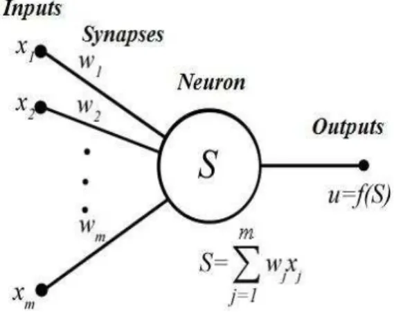
A synapse is an element that performs a weighed
signal transfer (1) from the neuron of one layer to the
neuron of the next layer within an artificial neural
net-work (figure 1).
f
(
x
)
w
∙
x
,
(1)
where
f
(
x
)
–
input of the neuron,
w
–
weights of the
synapse,
x
–
output of the previous neuron.
G.A. M
ELNIKOV,
N.M. I
GNATENKO,
V.G. M
ELNIKOVJ.
N
ANO-
E
LECTRON.
P
HYS.
8, 03023 (2016)
03023-3
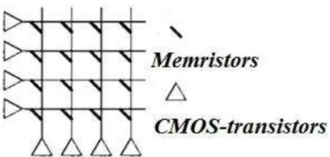
Fig. 2 – A fragment of the computing memristor crossbar ar-ray controlled by CMOS transistorsA memristor is a passive element in
microelectron-ics; its resistance depends on a charge that has passed
through it. When a voltage in the circuit is turned off, a
memristor doesn’t change its state and it registers the
last resistance value [9]. The following equations
de-scribe the voltage-current characteristic (2) and
re-sistance (3) of a memristor:
( )
( )
( )
Ron w t
1
w t
( )
v t
Roff
I t
D
D
,
(2)
d
R
S
,
(3)
where
v
(
t
)
–
voltage,
I
(
t
)
–
current,
w
(
t
)
–
thickness of
memristor’
s doped region,
D
–
total thickness of a
memristor,
Ron
–
the minimum resistance value of a
memristor,
Roff
–
the maximum resistance value of a
memristor,
R
–
resistance, ρ
–
resistivity of the
materi-al,
d
–
thickness of the active layer,
S
–
contact surface.
As for an environment for the experiment, we chose
a tool for modeling and simulating physical objects
–
the
«
Simscape
»
application software package that is
controlled by the
«
Matlab
»
. We synthesized simscape
memristor models (figure 3) which constituted a
two-layer feedforward neural network in the shape of a
crossbar array; its schematic visualization is shown in
figure 2. Its function is to approximate the differential
equation (4):
( )
ln( )
f x
a b
x
.
(4)
The artificial neural network was trained with the
help of Neural Network Toolboxes, after that the
ob-tained weighing coefficients were recorded in the
syn-apse model, so that the crossbar array could be used as
a computing system. The system’s maximum accur
acy
of operation was achieved when there were 17 neurons
in the first layer and one output neuron in the second
layer. The neuron activation functions
–
the hyperbolic
tangent sigmoid transfer function in the first layer and
the linear transfer function in the second one. The
training algorithm
–
Levenberg-Marquardt
backpropa-gation. Approximate error (sum squared error
perfor-mance function) amounted to 8.52
10
– 13.
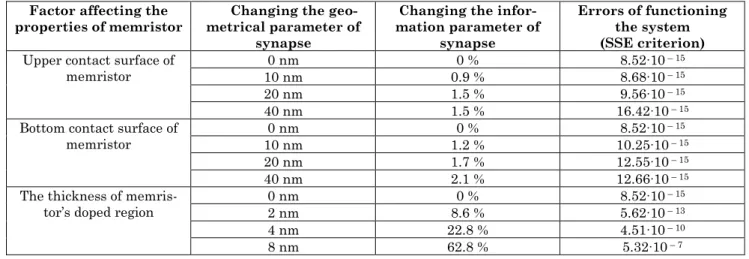
We revealed a number of factors impacting the
ma-terial properties: the top contact surface, the bottom
contact surface and the thickness of the dielectric layer.
The array was programmatically exposed to alteration
of the qualitative value of the factors at various levels.
On each stage of alteration of the properties of the
memristors
the qualitative alteration of the system’s
element parameters and the fault tolerance parameter
of the system as a whole were registered.
The research findings show that the
above-mentioned physical phenomena and processes in
na-noscale electronic elements which carry information in
the simulated artificial neural network, determine the
fault tolerance parameter of the system in question.
This is due to the fact that the element properties
im-pact their information parameters that determine the
system’s accuracy of operation. Therefore, analysis of
the properties, which characterize the reliability of
na-noscale electronic elements used for constructing data
processing systems, based on the idea that data should
be considered as an object for the conversion in the
stated systems, is the most promising and it enables us
to take into account all the factors that predetermine
the reliability parameter under examination. Table 1
shows the general research results.
G.A. M
ELNIKOV,
N.M. I
GNATENKO,
V.G. M
ELNIKOVJ.
N
ANO-
E
LECTRON.
P
HYS.
8, 03023 (2016)
03023-4
Table 1 – The experimental results of studying the proposed methodology using the model of an artificial neural network approx-imating a deferential equation as an example
Factor affecting the
properties of memristor
Changing the
geo-metrical parameter of
synapse
Changing the
infor-mation parameter of
synapse
Errors of functioning
the system
(SSE criterion)
Upper contact surface of
memristor
0 nm
0 %
8.52
∙
10
– 1510 nm
0.9 %
8.68
∙
10
– 1520 nm
1.5 %
9.56
∙
10
– 1540 nm
1.5 %
16.42
∙
10
– 15Bottom contact surface of
memristor
0 nm
0 %
8.52
∙
10
– 1510 nm
1.2 %
10.25
∙
10
– 1520 nm
1.7 %
12.55
∙
10
– 1540 nm
2.1 %
12.66
∙
10
– 15The thickness of
memris-tor’s doped region
0 nm
0 %
8.52
∙
10
– 15
2 nm
8.6 %
5.62
∙
10
– 134 nm
22.8 %
4.51
∙
10
– 108 nm
62.8 %
5.32
∙
10
– 74.
CONCLUSIONS
In the course of the research we achieved its goal
and met all the set targets. Here are some of the main
findings:
we proposed a theoretical and practical approach to
the practical analysis of the properties of nanoscale
electronic hardware components in order to determine
the quantitative and qualitative correlation among
them and technical parameters of the facilities made on
their basis;
we developed a methodology which makes it
possi-ble to determine the correlation between the fault
tolerance of a parallel computing system and a number
of properties of nanoscale electronic elements that are
present in the system in question.;
we experimentally examined the proposed
method-ology and as a result we determined the characteristics
of the nanoscale memristors, used as the synaptic links
of a neural network computing system, which
deter-mine the fault tolerance parameter.
ACKNOWLEDGEMENTS
The reported study was funded by RFBR, according
to the research project No. 16-37-60061 mol_
а
_dk.
REFERENCES
1. Л.А. и е , .А.Шах в, р ы р а :
а а а . 6, 57 (2013) (L.A. Zinchenko,
V.A. Shakhnov, Inzhenernyy zhurnal: nauka i innovatsii 6, 57 (2013)).
2. А. . а у и , р р а « р а в
ы ». Condens. Matter. 3 (2012) (A.I. Galushkin, Prilozheniye k zhurnalu «Info
r-matsionnyye tekhnologii»г Condensг Matterг 3 (2012)).
3. А. . а у и , р а ы 4, 2 (2014)
(A.I. Galushkin, Informatsionnyye tekhnologi 4, 2 (2014)). 4. S. Spiga, International Interconnect Technology Conference
and Materials for Advanced Metallization Conference (IITC/MAM), 213 (Grenoble: IEEE: 2015).
5. R.P. Shukla, G. Jain, S. Chandra, A. Ranjan, Futuristic Trends on Computational Analysis and Knowledge Man-agement (ABLAZE), 102 (New Delhi: IEEE: 2015). 6. D. Newberry, Nanotechnology (IEEE-NANO), 800
(Port-land: IEEE: 2011).
7. C. Yakopcic, R. Hasan, T.M. Taha, National Aerospace and Electronics Conference (IEEE-NAECON 2014), 243
(Dayton: IEEE: 2014).
8. K.-H. Kim, S. Gaba, D. Wheeler, J.M. Cruz-Albrecht, T. Hussain, N. Srinivasa, W. Lu, Nano Lett. 12, 389
(2012).