Brazilian Microwave and Optoelectronics Society-SBMO received 21 Dec 2016; for review 22 Dec 2016; accepted 29 Jan 2018 Abstract—We use the two dimensional finite element method
(2D-FEM) in the frequency domain to characterize the transmission properties of 900-bend periodic segmented waveguides (PSWs). We investigated the dependence of the transmission coefficient and the mode profile of PSWs on the bending radius, the waveguide duty cycle, and the operating wavelength. We show that 900-bend PSWs can be designed in photonic integrated circuits with a curvature radius as small as three times the wavelength to achieve transmission coefficient greater than 0.8.
Index Terms—Bend waveguide, finite element, mode profile, periodic segmented waveguide.
I. INTRODUCTION
Waveguide bending is necessary in the interconnections of photonic integrated circuits. Photonic
crystal waveguides (PCW) are good candidates for the design of photonic integrated circuits because
PCWs can be designed to guide light [1] with low losses. However, PCWs also have some limitations.
Since guiding path of a PCW is restricted by the periodicity of its geometry, it cannot be bent
arbitrarily [1]. On the other hand, it has been demonstrated that periodic segmented waveguides
(PSW) with sub wavelength periodicity exhibit high transmission and low losses [2-9]. A 900-bend
PSW can be manufactured with arbitrary shape while preserving high transmission [10-11].
In previous studies, we showed that the two dimensional finite element method (2D-FEM) in the
frequency domain can be used to efficiently model the transmission characteristics of the PSWs
[11,13]. We have studied the transmission characteristics of straight PSWs and compared them
against their equivalent straight continuous waveguide (CWG). In this paper, 900-bend PSWs are
Analysis of the Propagation Properties of 90
0
-bend Periodic Segmented Waveguides Using
the 2D Finite Element Method
C. E. Rubio-Mercedes,
State University of Mato Grosso do Sul, Mathematics and Engineering Physics Programs, Dourados, MS, Brazil, 79804-970, E-mail: [email protected]
V. F. Rodríguez-Esquerre,
Federal University of Bahia, Department of Electrical Engineering, Salvador, BA, Brazil, 40210-630, E-mail:[email protected]
I. T. Lima Jr.,
North Dakota State Universit, Department of Electrical and Computer Engineering,Fargo, ND, USA, 58108– 6050, E-mail: [email protected]
H. E. Hernández-Figueroa
simulated using the 2D-FEM in the frequency domain [11-14]. In contrast to the 900-bend PCW, the
light in a 900-bend PSW is confined to the core, which has an average refractive index higher than that
in the cladding material as in conventional 900-bend CWG structures.
II. SYSTEM DESCRIPTION AND METHOD OF ANALYSIS
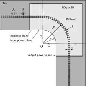
The Schematic of a 2D 900-bend PSW structure is shown in Fig. 1. R is the curvature radius, Λ is
the periodicity of the PSW, a represents the segment length, and the duty cycle η is defined as the
ratio between the length of the high index segment and the period, η = a/Λ. The Perfectly Matched
Layers (PML) for periodically varying structures [14] is used to limit the computational domain.
Λ a SiO2or SU
PML
O
y
z
R
r
Si
w
output power plane input power plane
incidence plane
90obend
Fig. 1 Schematic of 2D 900-bend PSW structure. Λ is the period, η is the duty cycle, and R the curvature radius of the 900 -bend PSW.
The material refractive indices of the 900- bend PSW are nSi = 3.476 for the waveguide core
segments, and nSi02 = 1.444 or nSU-8 = 1.577 for the waveguide cladding [2]. The periodicity of the
PSW is Λ = 300 nm, with segment width w = 300 nm, and segment length a = 150 nm (duty cycle η =
0.5).
The computational domain is on the plane z×y = (R + 4 µm + dPMLleft+ dPMLrigth) × (R + 4 µm +
dPMLtop+ dPMLbottom) where the PML thicknesses are 4.05 µm at the input and output ports, dPMLleft and
dPMLbottom, respectively, and 0.5 µm at the top and the right boundaries, dPMLtop.and dPMLrigth,
respectively. The point O is located at the coordinates (z, y) = (0, 5 µm - R). The center of the
horizontal and vertical PSWs are located along y = 5 µm and z = R, where r = R - 2 µm. The
excitation signal to the PSW is the fundamental mode of the equivalent CWG, which is placed at the
center of the closest segment to the left PML. The input and output mode fields and powers are
monitored at the planes located at the center of the second segment before the beginning of the 900-
bend, and at the center of the segment before the bottom PML, respectively.
Wave propagation in a PSW, such as the one schematically shown in Fig. 1 is described by the
Brazilian Microwave and Optoelectronics Society-SBMO received 21 Dec 2016; for review 22 Dec 2016; accepted 29 Jan 2018 (1)
where for TM waves φ = Ex, p = 1r, q = n2 and for TE waves φ = Hx , p = 1/n2, q = 1 and n(z,y) is
the refractive index of the waveguide that has an abrupt longitudinal variation in 900-bend PSWs.
For wavelengths far away from the band gap, a structure of 900-bend PSW, as given in Fig. 1, is
equivalent to a 900-bend CWG with the same depth and same width but with refractive index given
by[2], [6-8], [11-12]
(2)
where nclad is the cladding index, η is the duty cycle and ∆n = nmax - nclad, is the refractive index
contrast.
Applying the Galerkin procedure [13-14] to (1), the following matrix equation is obtained
(3)
where [A] is the resulting assembled global matrix of the 2D-FEM given by
(4)
where β is the effective propagation constant of the waveguide, and [B] is the resulting matrix of
the one dimensional (1D) FEM applied in the incidence plane, which is given by
(5)
{φinc} is the incident field, and the parameters sz, sy, and s are constants due to the use of PML
domains [13-14].
The meshes used are dependent on the bending radius, which lies in the interval from 3 µm to 10
µm. The meshes have between 37,000 and 47,000 triangular quadratic elements and between 77,000
and 95,696 nodes. The convergence in each simulation was verified for each mesh used to discretize
the simulation domain.
III. NUMERICAL RESULTS
We study the transmission properties of a 900-bend PSW and compared it against the equivalent
CWG calculating the overlap integral and the confinement factor of the modes. In all the cases
simulated we consider silicon (Si) for the core segments and silica (SiO2) or SU-8 for the cladding in
the waveguides.
First, we calculate the mode profiles of 900-bend PSWs, with curvature radius R = 5 µ m, operating
[ ]
{ } { }
{ } { }
k qs{ }{ }
N N dydzy N y N s s p + z N z N s s p = A e e Ω T T y T z
− ∂ ∂ ∂ ∂ ∂ ∂ ∂ ∂ 2 0 2 2[ ]
{ }{ }
e e z ' dy N N s s p = B 2 0 = φ qsk + z φ s p z s + y φ s p ys 02
z z y y ∂ ∂ ∂ ∂ ∂ ∂ ∂ ∂
[ ]
A
{ }
φ
=
−
2
j
β
[ ]
B
{ }
φ
incηΔ
n
+
n
=
wavelength λ = 1550 nm, and TE polarization. The refractive indexes of the equivalent CWG are neq = 2.46 for
silica cladding and neq = 2.5265 for SU-8 cladding, respectively [2]. We compare the mode profiles of the 900
-bend PSWs with the mode profiles of their equivalent 900-bend CWGs by calculating the overlap integral, the
confinement factor, and the transmission coefficient of the modes. We consider silicon (Si) for the core
segments and silica (SiO2) or SU-8 for the cladding in the waveguides. The refractive index of the equivalent
CWG is calculated using the same procedure applied in previous studies [2-5]. We calculate the overlap integral
of the 900-bend PSW mode profile with a wire CWG (equivalent to a straight PSW with duty cycle η = 1.0)
mode profile with widths varying from 160 nm to 300 nm. The results are shown in Figs. 2 and 3. The overlap
integral of the mode profiles of 300 nm wide 900-bend PSW and the mode of the equivalent 160 nm wide CWG
is approximately equal to 96% for silica and SU-8 cladding materials with the confinement factor Г = 51% for
both cases. If we consider a CWG of width w = 300 nm, the overlap integral is equal to 83% and 85% for SU-8 for silica and SU-8 cladding, respectively, and the confinement factor Г = 75% for both claddings. In Fig. 2, we
also show the overlap integral of the mode in the 300 nm wide 900-bend PSW with the mode of an equivalent
wire CWG (equivalent to a straight PSW with duty cycle η = 0.5) with widths varying from 160 nm to 300 nm.
We observe that the overlap integral of the mode profile of the 300 nm wide 900-bend PSW with the mode of
the equivalent CWG with the same width (300 nm) is equal to 98% and 97% for silica and SU-8 cladding,
respectively, while the overlap integral drops only to 84%, for both cladding materials, when the 300 nm wide
PSW mode profile is compared with the mode of a 160 nm wide equivalent CWG. In Fig. 4, we show the
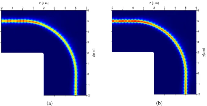
simulated results of the intensity of the propagating field in the 900-bend PSW structure for (a) silica cladding
and for (b) SU-8 cladding.
160 190 220 250 280 310 340
81 84 87 90 93 96 99
CWG (ncoore= nSi) CWG (ncoore= neq)
O
v
e
rl
a
p
I
n
te
g
ra
l
(%
)
Waveguide width w [nm]
Cladding Silica SU-8
Fig. 2 Overlap integral of the output 900- bendPSW mode profile with a CWG mode profile with different waveguide widths and considering its core as being Si or being the equivalent material of the PSW (neq = 2.46 for silica cladding and neq =
Brazilian Microwave and Optoelectronics Society-SBMO received 21 Dec 2016; for review 22 Dec 2016; accepted 29 Jan 2018
160 180 200 220 240 260 280 300 320 50
55 60 65 70 75 80
C
o
n
fi
n
e
m
e
n
t
F
a
c
to
r
Γ
(%
)
Waveguide Width W[nm] Cladding
Silica SU-8
Fig. 3 Confinement factor of the steady-state 900- bend PSW mode profile as a function of the waveguide width.
-2 -1 0 1 2 3 4 5 6
z [µ m]
-2 -1 0 1 2 3 4 5 6
y
[
µ
m
]
-2 -1 0 1 2 3 4 5 6
z [µ m]
-2 -1 0 1 2 3 4 5 6
y
[
µ
m
]
(a)
(b)
Fig. 4 Intensity field profiles along 900-bend PSWs. R = 5 µm, Λ= 300 nm, η= 0.5, and w = 300 nm with Si in the core and (a) Silica and (b) SU-8 in the claddings.
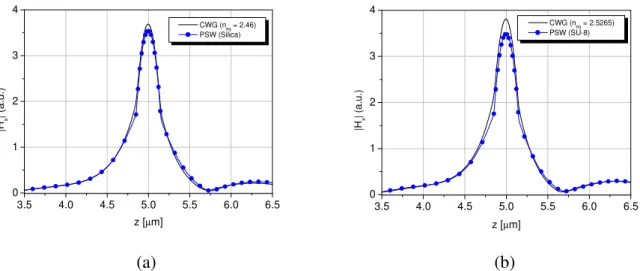
In Fig. 5, we show the transversal mode profiles at the output of 900-bend PSWs with their
equivalent 900-bend CWGs using (a) silica and (b) SU-8 claddings. The black line in Fig. 5 represents
the equivalent 900-bend CWG mode profile whereas the blue line in Fig. 5 (a) and (b) represent the
silica and SU-8 claddings, respectively. The transmission coefficients, calculated as the ratio of the
output and input powers, are 0.8 for silica cladding and 0.7 for SU-8 cladding for the parameters used
in Fig. 5. These results indicate that, for the duty cycle η = 0.5, the 900-bend PSW with silica cladding
can be better approximated by their equivalent 900-bend CWG than the 900-bend PSW with SU-8
3.5 4.0 4.5 5.0 5.5 6.0 6.5 0
1 2 3 4
|H
x
|
(a
.u
.)
z [µm]
CWG (neq = 2.46)
PSW (Silica)
3.5 4.0 4.5 5.0 5.5 6.0 6.5
0 1 2 3 4
|H
x
|
(a
.u
.)
z [µm]
CWG (neq = 2.5265)
PSW (SU-8)
(a)
(b)
Fig. 5 Transversal output field profiles o 900-bend PSWs and their equivalent 900-bend CWG using refractive indexes (a) nclad = 1.444, ncore = 2.46 for silica cladding and (b) nclad = 1.577, ncore = 2.5265 for SU-8 cladding, respectively.
We then compared the transmission properties of 900-bend PSWs with their equivalent 900-bend
CWGs as a function of the period Λ the duty cycle η and the radius R. To do so, we carried out three
parameter studies:
Variation of period Λ from 280 nm to 440 nm for η = 0.5 and radius R = 5 µm
Variation of the duty cycle η from 0.1 to 1.0 for period Λ =300 nm and radius R = 5 µm
Variation of the curvature radius R from 3 µm to 10 µm for duty cycle η = 0.5 and period Λ =300
nm.
A. Dependence on period
In Fig. 6, we show the transmission coefficients of 900-bend PSWs as a function of the period for
the wavelength λ =1550 nm for silica cladding (red line) and SU-8 cladding (blue line). In this study,
the curvature radius and duty-cycle of the 900-bend PSWs are fixed at R = 5 µm and η = 0.5. The
period Λ of the PSWs varies from 280 nm to 440 nm, the waveguide width is w = 300 nm, and the
refractive indexes of the segments are nSi = 3.476. We observed that the transmission coefficient of
the 900-bend PSW starts decreasing slowly when the period increases and it rapidly decays when the
period Λ is longer than 340 nm for SiO2 cladding and longer than 360 nm for SU-8 claddings. These
results suggest that the subwavelength operation regime is no longer satisfied when the period Λ
exceeds the respective threshold for each of these two cases, since the waveguides reached the Bragg
condition in these cases.
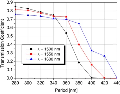
In Fig. 7, we show the transmission coefficient as a function of the period for three different
wavelengths: λ = 1500 nm (black line), λ = 1550 nm (red line), and λ = 1600 nm (blue line), in which
only silica cladding 900-bend PSWs are considered. We observed that the transmission coefficient in
the 900-bend PSWs with silica cladding rapidly reduces for periods Λ larger than about 340 nm when
Brazilian Microwave and Optoelectronics Society-SBMO received 21 Dec 2016; for review 22 Dec 2016; accepted 29 Jan 2018 to drop when Λ = 380 nm. This behavior can be explained as follow: In general, power confinement
into the core of the 900-bend PSW increases as the wavelength λ decreases (silica cladding). This
means that the light propagating through the core of the 900-bend PSW is more likely to be diffracted
as the wavelength λ decreases. Therefore, the smaller the wavelength λ, the more sensitive to the
period Λ the field is. The results shown in Fig. 6 and 7 indicate that it is desirable to keep the 900
-bend PSW period Λ lower than about 300 nm to obtain a transmission coefficient greater 0.8 for silica
claddings at wavelengths λ smaller than 1550 nm.
280 300 320 340 360 380 400 420 440 0.0
0.1 0.2 0.3 0.4 0.5 0.6 0.7 0.8 0.9
T
ra
n
s
m
is
s
io
n
C
o
e
ff
ic
ie
n
t
Period [nm] Silica
SU-8
Fig. 6 Transmission coefficient of the 900-bend PSWs as a function of the period Λ. η= 0.5, R = 5 µm, w = 300 nm, core index nSi = 3.476, and wavelength λ = 1550 nm. Two different cladding materials are considered: Silica (red line) and SU-8
(blue line).
280 300 320 340 360 380 400 420 440 0.0
0.1 0.2 0.3 0.4 0.5 0.6 0.7 0.8 0.9
T
ra
n
s
m
is
s
io
n
C
o
e
ff
ic
ie
n
t
Period [nm] λ = 1500 nm
λ = 1550 nm λ = 1600 nm
B. Dependence on duty cycle
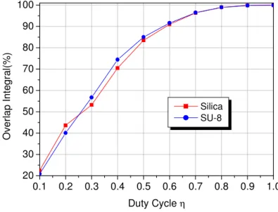
In Fig. 8, we show the overlap integral between the modes of 900-bend PSW (φPSW) and CWG
(φCWG) as a function of the duty cycle for the wavelength λ = 1550 nm for two different cladding
materials: Silica (red line) and SU-8 (blue line). The curvature radius and period of 900-bend PSW are
fixed R = 5 µm and Λ = 300 nm. Therefore, total number of segments is kept constant when the duty
cycle varies from η = 0.1 to 1.0. We observe that the overlap integral for duty cycles between η = 0.3
and η = 0.6 the SU-8 cladding is larger than the overlap integral of silica cladding. However, we
observed that the power loss increases rapidly in both cases with the decrease of the duty cycle.
0.1 0.2 0.3 0.4 0.5 0.6 0.7 0.8 0.9 1.0 20
30 40 50 60 70 80 90 100
O
v
e
rl
a
p
I
n
te
g
ra
l(
%
)
Duty Cycle η
Silica SU-8
Fig. 8 Overlap integral between φPSW and φCWG modes as a function of the duty cycle. Λ = 300, R = 5 µm, and w = 300 nm. Two different cladding materials are considered: Silica (red line) and SU-8 (blue line).
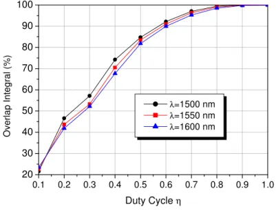
In Fig. 9, we show the overlap integral between 900-bend φPSW and φCWG modes as a function of the
duty cycle for tree different wavelengths: λ = 1500 nm (black line), 1550 nm (red line), and 1600 nm
(blue line), in which only silica cladding 900-bend PSWs are considered. We observed in Figs. 8 and 9
that the overlap integral between 900-bend PSW and the CWG modes increases to 100% with the duty
cycle and rapidly reduces for duty cycles shorter than 0.6. Therefore, 900-bend PSWs with larger duty
cycle are more effective. We did not observe a significant dependence of the overlap integral and,
Brazilian Microwave and Optoelectronics Society-SBMO received 21 Dec 2016; for review 22 Dec 2016; accepted 29 Jan 2018
0.1 0.2 0.3 0.4 0.5 0.6 0.7 0.8 0.9 1.0 20
30 40 50 60 70 80 90 100
O
v
e
rl
a
p
I
n
te
g
ra
l
(%
)
Duty Cycle η
λ=1500 nm λ=1550 nm λ=1600 nm
Fig. 9 Overlap integral between φPSW and φCWG modes as a function of the duty cycle. Λ = 300, R=5 µm, and w = 300 nm. Three different wavelengths are considered: λ = 1500 nm (black line), λ = 1550 nm (red line) λ = 1600 nm (blue line).
C. Dependence on the curvature radius
In Fig. 10 we show the overlap integral between 900-bend PSW and CWG modes and the
transmission coefficient as a function of wavelength for two different cladding materials: Silica and
SU-8. In this parameter study, the period Λ = 300 nm, segment width w = 300 nm, duty cycle η= 0.5,
and R = 5 µm are fixed. The blue line represents the overlap integral of the 900-bend PSW with silica
cladding and the black lines represent the overlap integral as a function of wavelength for SU-8
cladding. For λ = 1420 nm and λ = 1600 nm, the overlap integral values are 98% and 93% for both
silica and SU-8 cladding materials, respectively
.
1.40 1.42 1.44 1.46 1.48 1.50 1.52 1.54 1.56 1.58 1.60 84
86 88 90 92 94 96 98 100
O
v
e
rl
a
p
I
n
te
g
ra
l
(%
)
Wavelength [µm]
Silica SU-8
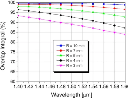
In Fig. 11, we show the overlap integral as a function of wavelength for Silica cladding and
five curvature radius values. The curvature radius values are R = 10 µm (blue line), R = 7 µm (red
line), R = 5 µm (green line), R = 4 µm (black line), and R = 3 µm (magenta line). The material
refractive indices are: nSi = 3.476 for the core segments, and nSiO2 = 1.444 for the waveguide
claddings. We observed that, for the entire wavelengths range shown in Fig. 11, the overlap integral is
greater than 97% for curvature radii R equal to 7 µm and 10 µm, while the overlap integral is greater
than 93% for curvature radius R = 5 µm. When the curvature radius is as small as 3 µm, the overlap
integral drops down to 84% at λ = 1600 nm. Therefore, PSWs can tolerate sharp bends with relatively
low losses
.
1.40 1.42 1.44 1.46 1.48 1.50 1.52 1.54 1.56 1.58 1.60
60 65 70 75 80 85 90 95 100
O
v
e
rl
a
p
I
n
te
g
ra
l
(%
)
Wavelength [µm]
R = 10 mm R = 7 mm R = 5 mm R = 4 mm R = 3 mm
Fig. 11 Overlap integral between φPSW and φCWG modes as a function of wavelength. η = 0.5, Λ=300, and w = 300 nm. Five different curvature radius values are considered: R = 10 µm (blue line), R = 7 µm (red line), R = 5 µm (green line), R = 4 µm
(black line) and R = 3 µm (magenta line) for SiO2 cladding.
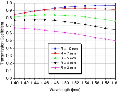
In Fig. 12, we show the transmission coefficient of 900-bend PSWs for five curvature radius values:
R = 10 µm (blue line), R = 7 µm (red line), R = 5 µm (green line), R = 4 µm (black line), and R = 3
µm (magenta line), as a function of wavelength for Silica cladding. In this figure, we observed that, at
the wavelength λ = 1600 nm, the transmission coefficients are 0.97 and 0.91 for curvature radii R = 10
µm and R = 7 µm, respectively. For a curvature radius R = 5 µm and for the wavelengths λ = 1400
nm and λ = 1600 nm, the transmission coefficient values are 0.81 and 0.76, respectively, and with the
maximum value of 0.84 at λ = 1460 nm. We concluded that the curvature radius of the 900-bend PSW
Brazilian Microwave and Optoelectronics Society-SBMO received 21 Dec 2016; for review 22 Dec 2016; accepted 29 Jan 2018
1.40 1.42 1.44 1.46 1.48 1.50 1.52 1.54 1.56 1.58 1.60 0.0
0.1 0.2 0.3 0.4 0.5 0.6 0.7 0.8 0.9 1.0
T
ra
n
s
m
is
s
io
n
C
o
e
ff
ic
ie
n
t
Wavelength l[mm]
R = 10 mm R = 7 mm R = 5 mm R = 4 mm R = 3 mm
Fig. 12 Transmission coefficient of 900-bend PSWs as a function of wavelength and for η = 0.5, Λ=300, and w = 300 nm. Five different curvature radius values are considered: R= 10 µm (blue line), R = 7 µm (red line), R = 5 µm (green line), R =
4 µm (black line), and R = 3 µm (magenta line) for SiO2 cladding.
IV. CONCLUSIONS
We used the 2D-FEM in the frequency domain to show that PSWs can be used to design photonic
integrated circuits with sharp 900-bends. To demonstrate the effectiveness of PSWs, we calculated the
overlap integral and the confinement factor of 900-bend PSWs mode profile with equivalent wire
CWGs mode profile with widths varying from 160 nm to 300 nm. We showed that the mode profile of
a 900-bend PSW is comparable to the mode profile of the equivalent 900-bend CWG even for
relatively high values of averaged refractive index contrast. We also calculated the transmission
coefficient as a function of the period Λ and the overlap integral as a function of the duty cycle η for
900-bend PSWs with two different cladding materials: Silica and SU-8. In the waveguides that we
studied, we concluded that the period Λ should not exceed 320 nm for λ ≈ 1500 nm to obtain a
transmission coefficient greater than 0.8, and that the optimum value to be chosen for the duty cycle is
η = 0.5 for silica cladding and η = 0.6 for SU-8 cladding [2]. We also concluded that the curvature
radius of a 900-bend PSW should be larger than 3λ to obtain a transmission coefficient greater than
0.8. We observed that the transmission coefficients of a 900-bend PSWs is 0.91 at λ = 1600 nm for a
curvature radius as small as R = 7 µm.
The simulation of crossings and the nonlinear formulation of PSW are under analysis and results
will be report in a near future.
ACKNOWLEDGMENT
This work was supported in part by the CAPES (Process number 3724/10-7), CNPq (INCT Fotonicom
REFERENCES
[1] K. Sakoda, Optical Properties of Photonic Crystals, Springer Verlag, New York (2001).
[2] P. J. Bock, P. Cheben, J. H. Schmid, J. Lapointe, A. Delâge, S. Janz, G. C. Aers, D-X Xu, A. Densmore and T. J. Hall, Subwavelength grating periodic structures in silicon-on-insulator: a new type of microphotonic waveguide, Opt. Express, 18 (2010) 20251.
[3] M. Gnan, S. Thoms, D. S. Macintyre, R. M. De La Rue, and M. Sorel, Fabrication of low-loss photonic wires in silicon-on-insulator using hydrogen silsesquioxane electron-beam resist, Electron. Lett. 44 (2008) 115.
[4] W. Śmigaj, P. Lalanne, J. Yang, T. Paul, C. Rockstuhl and F. Lederer, Closed-form expression for the scattering coefficients at an interface between two periodic media, Appl. Phys. Lett. 98 (2011) 111107.
[5] Z. Weissman and A. Hardy, Modes of Periodically Segmented Waveguide, J. Ligthwave Technol. 11 (1993) 1831. [6] D. Nir, Z. Weissman, S. Ruschin and A. Hardy, Periodically segmented waveguide in Ti: LiNbO3, Opt. Lett. 19 (1994)
1732.
[7] D. Ortega, R. M. De la Rue, and J. S. Aitchison, Cutoff Wavelength of Periodically Segmented Waveguides in Ti:LiNbO3, J. Ligthwave Technol. 16 (1998) 284.
[8] D. Ortega, J. M. Aldariz, J. M. Arnold and J. S. Aitchison, Analysis of “Quasi-Modes” in Periodic Segmented Waveguides, J. Ligthwave Technol. 17 (1999) 369.
[9] P. Luan and K. Chang, Transmission characteristics of finite periodic dielectric waveguides, Opt. Express, 14 (2006) 3263.
[10]K-Y Lee, C-N Chen, Y-J Lin, Transmission characteristics of various bent periodic dielectric waveguides, Opt. Quant. Electron, 40 (2008) 633.
[11]C. E. Rubio-Mercedes, Ivan T. Lima, Jr, H. E. Hernández-Figueroa, and V. F. Rodríguez-Esquerre, Periodic segmented waveguide analysis by using the 2D finite element method, in SBMO/IEEE MTT-S International Microwave & Optoelectronics Conference (IMOC), (2011) 876 [doi:10.1109/IMOC.2011.6169297].
[12]C. E. Rubio-Mercedes, V. F. Rodríguez-Esquerre, Ivan T. Lima, Jr and H. E. Hernández-Figueroa, Analysis of straight periodic segmented waveguide using 2D finite element method, J. Lightwave Technol. 32 (2014) 1114.
[13]C. E. Rubio-Mercedes e H. E. Hernández-Figueroa, Padé boundary conditions for the finite-element solution of arbitrary planar junctions, J. Lightwave Technol. 22 (2004) 669.