Planar Non-volatile Memory based on Metal Nanoparticles.
Journal: 2011 MRS Spring Meeting Manuscript ID: MRSS11-1337-Q10-05.R1 Manuscript Type: Symposium Q
Date Submitted by the Author: n/a
Complete List of Authors: Kiazadeh, Asal; Algarve university, CEOT
Gomes, Henrique; Algarve university, CEOT; Algarve university, CEOT
Da costa, Ana; Algarve university, CEOT Rocha, Paulo; Algarve university, CEOT Chen, Qian; Algarve university, CEOT Moreira, Jose; Algarve university, CEOT de Leeuw, Dago; Philips
Meskers, Stefan; TUe, Chemical eng. Keywords: electrical properties, nanostructure, Ag
Planar Non-Volatile Memory based on Metal Nanoparticles
A. Kiazadeh1, H. L. Gomes1, A. R. Da Costa2, J. A. Moreira2, D. M. De Leeuw3 and S. C. J. Meskers 4
1
Center of Electronics Optoelectronics and Telecommunications (CEOT)
2
Centro de Investigação em Química do Algarve
Universidade do Algarve, Campus de Gambelas, 8000-139 Faro, Portugal,
3 Philips Research Laboratories, High Tech Campus 4 WAG 11, 5656 AE Eindhoven, The
Netherlands
4 Molecular Materials and Nanosystems, Eindhoven University of Technology, P.O. Box 513,
5600 MB Eindhoven, The Netherlands ABSTRACT
Resistive switching properties of silver nanoparticles hosted in an insulating polymer matrix (poly(N-vinyl-2-pyrrolidone) are reported. Planar devices structures using interdigitated gold electrodes were fabricated. These devices have on/off resistance ratio as high as 103 , retention times reaching to months and good endurance cycles. Temperature-dependent measurements show that the charge transport is weakly thermal activated (73 meV) for both states suggesting that nanoparticles will not aggregate into a metallic filament.
INTRODUCTION
Metal-Insulator-Metal (MIM) structures where the insulator layer is comprised of metal nanoparticles (Nps) or nanostructured metal films embedded in semiconductive or semi-insulating host matrices have attracted considerable attention due to their interesting electrical properties and because of their potential for high density non-volatile memory applications. These devices show dramatic changes of the electrical resistance, so-called resistive switching effect. Current-voltage characteristics switch reversibly between a low conductance off-state and a high conductance on-state [1-7]. This phenomenon has being intensively investigated
worldwide for developing Resistive Random Access Memories (RRAMs), a possible competitor, and even replacement for flash memory and hard-disk drives. It is relatively easy to produce
colloidal solutions a well-defined contribution of nanoparticles and polymers, and it is the advantage of nanoparticles based systems. Thin films can be deposited by spin-coating, printing, or dip-coating techniques offering the prospect of low fabrication cost, mechanical flexibility and light weight.
In spite of intense efforts, the detailed physics of the resistive switching is still not elucidated. The majority of the work reported in literature, is for sandwich type structures where one of the electrodes is often a reactive metal such as aluminum [8]. This makes difficult to discriminate interfacial effects occurring at the electrode/material interface from bulk process. In this contribution, we fabricate a planar structure using interdigitated gold electrodes. The resistive switching channel is comprised of silver nanoparticles embedded into an insulating polymer matrix. This planar structure is much simpler than sandwich structures and may contribute to elucidate the detailed physics of the resistive switching phenomena. Furthermore, planar structures have a significant lower intrinsic capacitance than sandwich structures, therefore, they should have a faster dynamic response. In addition, planar structures have the active layer
directly exposed and can be probed by a number of surface analytical techniques to identify and characterize topographical, morphological changes that occur in the devices upon resistive switching.
EXPERIMENT
Poly (N-vinyl-2-pyrrolidone) (PVP, MW=25000) was supplied by Fluka. Other chemicals were purchased from Merck and used without any further purification. Ultraviolet absorption spectrum measurements were carried out with an (Shimadzu-UV 2550-8030) Spectrophotometer. Transmission Electron Microscopy (TEM) was performed with a CM-200 FEG Philips apparatus.
Silver nanoparticles were prepared by reducing the silver nitrate in poly-vinyl-pyrrolidone (PVP) aqueous solution. Dimethylformamid DMF was used as a reducing agent. The PVP solution was prepared by dissolving PVP in DMF and stirred at 300 rpm then AgNO3 solution with
considering 1:4 molar ratio of silver to PVP was added into the solution. The formation of silver nanoparticles was confirmed by UV-Vis spectrophotometer. The average size (25 nm) was estimated by transmission electron micrograph TEM. Figure 1 show the device test structure used to measure the electrical properties of the system comprised of nanocrystals in a semi insulating or insulating host matrix. A thin film is formed between the two gold electrodes on top of the insulating silicon dioxide surface by spin coating. Prior to electrical measurements the samples were also pumped in vacuum to remove further any residual solvent. Electrical measurements were carried out using a Keithley 487 picoammeter/voltage source in dark and in high vacuum conditions. To test the electrical properties of these structures we applied symmetrical voltage ramps with increasing voltage. During all the measurement the conductive silicon substrate is kept grounded to prevent charging of the SiO2 layer.
Figure 1 (a) TEM image of PVP capped silver nanoparticles (b) and planar device structure with 10 µm separated gold electrodes.
DISCUSSION
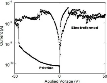
Initially, the system comprised of silver nanoparticles embedded in the PVP matrix behaves as an insulating or semi-insulating material. The corresponding current-voltage-characteristic is the lower curve represented in figure 2. The resistance at 10 V is approximately 10 G . This insulating state of the sample is named pristine state. Then suddenly, near 45 V the current rises dramatically and switch to the upper I-V characteristic represented in figure 2. This state is named electroformed state.
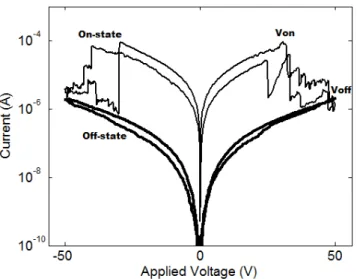
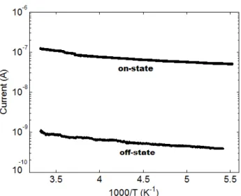
Figure 2 Current-voltage characteristics for the Pristine and the electroformed states. The change in device electrical properties from pristine state to more conductive state is irreversible if the device is kept under vacuum. This permanent modification corresponds to an electroforming process [9]. The nature of the electroforming process in nanoparticles-based systems is still not clear. After subsequently I-V loops the noisy I-V characteristic observed immediately after the switch from a pristine to an electroformed state (see figure 2), evolves to a noise free on-state characteristic with well-defined negative differentially resistance (NDR) regions located at around |35| V as represented figure 3. The local maximum and local minimum of its current is indicated as Von and Voff, respectively. The programming of the two conductive states is done by a voltage pulse with a length of a few seconds. The on and off-state can be set by voltages pulses of either polarity. A pulse near Voff will bring the device to the low conductance state or off-state. The high conductance curve (on-state) is restored by using a pulse near Von which is typical 30 V. The on/off ratio is almost 3 orders of magnitude as shown in figure 3. The memory is non-volatile. The retention time of both states was measured for a period of 10 days as shown in figure 4(a). The on/off ratio does not degrade with time. The cycle endurance represented in figure 4(b) was measured by programming successively the memory. The voltage pulse sequence used was as follow: write voltage (W) is 30 V and the erase (E) is 50 V. For both states the read voltage (R) is 3 V. The temperature dependence of the on and off states was measured in the temperature range of [320-200 K] with a continuous applied voltage of 3V after pulses near to Voff and Von for each state. The Arrhenius plot in figure 5 shows that the current is weakly thermally activate with single activation energy for both states of only ~73 meV.
Figure 3 Current-voltage characteristics for the on and off states. The on-state shows negative differential regions (NDR).
(a) (b)
Figure 4 (a) Retention time for both states measured at 3V (b) Cycles of endurance to show the programmable device at both on and off states. The write voltage (W) is 30V and the erase voltage (E) is 50V, for both states the read voltage (R) is 3V.
Although, it is low activation energy, it still suggests that metallic paths are not established between the electrodes; otherwise we would expect a non-activated behavior or even a positive temperature coefficient for the change in current. Switching has been reported in sandwich structures of AgI by Liag et al. [10] and for Ag2S by Waser and Aono [11]. Both reports treated the switching layer as a solid electrolyte where silver ion migration is claimed to occur with an electroactive electrode. Resistive switching is then readily explained by formation and rupture of metallic filaments. The findings in planar structures reported here seems to discharge this process, because the electrodes are considerable apart (10 µm).
Figure 5 Temperature dependence of the current for the on and off states measured at 3V. Furthermore, they are non-reactive gold electrodes; migration of metallic species from electrodes is unlikely to occur. It is interesting to point out that the switching behavior of these planar memory devices is similar to the switching behavior of sandwich type metal-oxide polymer diodes [12]. Both systems need an electroforming process; they show almost undistinguishable electrical properties, similar current-voltage characteristics with NDR regions, and equal programming features. This suggests that the underlying resistive switching mechanism is also similar. It is possible that the silver nanoparticles may form silver oxide clusters distributed within the polymer matrix. Therefore, the two switching systems become also physically similar. CONCLUSIONS
The electrical switching and memory effects of the device made from AgNPs/PVP film are investigated. The device can be switched between high and low conductance states by voltage pulses. The endurance characteristics were obtained for ~ 1000 programmed cycles with write and erase voltages of 30 V and 50 V, respectively. The retention time measurements show the memory states are stable for months when kept under vacuum. The on and off-states are stable for months as long as the device is kept under vacuum. Under ambient atmosphere it shows different switching hysteresis (unpublished data). The respective conductance states are volatile and unreliable, suggesting that they are related with surface electrical conduction mediated by moisture. The temperature measurements show that for both on and off states the current is weakly thermal activated, suggesting that metallic conduction does not occur in this structure. These devices are free of complex electrode interfaces, they have the conduction channel accessible to surface analytical techniques, therefore, they are an ideal tool to get insight into the fundamental aspects related how metallic nanoparticles contribute for the charge carrier trapping and transport in a insulating matrix.
ACKNOWLEDGMENTS
We gratefully acknowledge the financial support received from the Dutch Polymer Institute (DPI), project n.º 703, from Fundação para Ciência e Tecnologia (FCT) through the research Unit, Center of Electronics Optoelectronics and Telecommunications (CEOT), REEQ/601/EEI/2005 and the POCI 2010, FEDER
REFERENCES
1. L. D. Bozano, B. W. Kean, M. Beinhoff, K. R. Carter, P. M. Rice, J. C. Scott, J. Adv. Fun. Mater. 15, 1933 (2005)
2. G. Liu, Q. D. Ling, E. T. Kang, K. G. Neoh, D. J. Liaw, F. C. Chang, C. X. Zhu, D. S. H. Chan, J. Appl. Phys. 102, 024502 (2007)
3. S. Paul, A. Kanwal, M. Chhowalla, J. Nanotechnology, 17, 145 (2006)
4. H. S. Majumdar, J. K. Baral, R. Österbacka, O. Ikkala, H. Stubb, J. Org. Electron. 6, 188 (2005) 5. H.T. Lin, Z. Pei, Y. J. Chan, IEEE Electron Dev. Lett. 28, 569 (2007)
6. B. Pradhan, S. K. Batabyal, A. J. Pal, J. Phys. Chem. B. 110, 8274 (2006)
7. B. Cho, T. W. Kim, M. Choe, G. Wang, S. Song, R. Lee, J. Org. Electron. 10, 473 (2009) 8. J. C. Scott, L. D. Bozano, J. Adv. Mater. 19, 1452 (2007)
9. J. G. Simmons and R. R. Verderber, Proceedings of the Royal Society of London, Series A. 301, 77 (1967) 10. X. F. Liang, Y. Chen, L. Shi, J. Lin, J. Yin and Z. G. Liu, J. Phys. D: Appl. Phys. 40, 4767 (2007) 11. R. Waser and M. Aono, J. NatureMaterials. 6, 833 (2007)
12. F. Verbakel, S. C. J. Meskers, R. A. J. Janssen, H. L. Gomes, M. Cölle, M. Büchel, D. M. de Leeuw, J. Appl. Phys. Lett. 91, 192103 (2007)