Abstract— DC photocurrent gain properties of planar metal-semiconductor-metal (MSM) optical sensor structures on have been investigated experimentally. The test structure has two co-planar Mo/n-Si Schottky-barrier junctions on silicon of resistivity 9-12 Ω-cm and the electrode separation is 20 μm. The current-voltage (I-V) characteristics measurements under illumination in visible range showed a rapid increase in photocurrent at higher biases examined. From the temperature, the dependence of I-V characteristics and noise measurements, such photocurrent increase was ascribes to avalanche multiplication of carriers photogenerated in the Schottky junction reversed-biased. From low-frequency (10-50kHz) signal measurements, it was found that multiplication factor larger than 100 at 10kHz and 30 at 50kHz was achieved.
Index Terms— Planar metal-semiconductor-metal, Optical sensor, Photocurrent control, Shot noise.
I. INTRODUCTION
With an increasing demand of optical signal processing, planar metal-semiconductor-metal (MSM) optical sensor structures have attracted much attention as a viable structures for application to optoelectronics systems [1]. This structure provides some essential advantages: simpler fabrication process due to simple planar structure as well as ease for integration with other functions such as FETs. In addition, since silicon is the most extensively employed material for semiconductor devices, an internal photocurrent gain provided by avalanche multiplication is of interest for higher optical responsively. In the communication system, we have examined simple Si-based MSM optical sensor structures, aiming at static (dc) photocurrent enhancement.
II. EXPERIMENTAL
The samples were prepared as follows. We performed electron-beam evaporation of Mo film 3000 Å thick onto an n-type silicon of resistivity of 10 Ω-cm at an initial vacuum of evaporation was about 3×10⁻⁴ Pa onto an n-type silicon of resistivity of 10 Ω-cm. Mo film so formed works as Schottky-barrier metal to silicon and electrodes as well. The inset in Figure 1 shows the configuration of the sample, which was completed by photolithography lift-off technique. The size of both electrodes is the same (symmetrical) and of 3×3mm2.
Manuscript received December 24, 2008.
N. Atiwongsangthong and W. Titiroongruang are with Department of Electronics, Faculty of Engineering, King Mongkut's Institute of Technology Ladkrabang, Charongkrung Road, Ladkrabang, Bangkok, 10520 Thailand.
2 V 1
V 〈
Depleted Region
ELECTRODE SPACING
V
n-Si
CATHODE(Mo) ANODE(Mo)
INCIDENT LIGHT
9-12Ω−cm Neutral Region
Fig. 1. Schematic illustration of MSM structure having widely-separated electrodes under a bias.
The sample is single slit type (not interdigitated). The separation between the electrodes is 20 μm, which is wide enough for the two depletion regions of both junctions not to contact each other even when dc bias voltage is applied. Under a bias, the anode is forward-biased and the cathode is reversed-biased. Thus, the band diagram of the structure under a bias much larger than its built-in voltage is assumed a single junction. From the forward current-voltage (I-V) characteristics and capacitance-voltage (C-V) characteristics under dark of independent Schottky-barriers, the barrier height and built-in voltage were estimated to lie around 0.70 eV and 0.23 eV, respectively [2].
III. MEASUREMENT
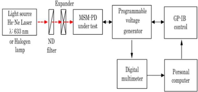
The current versus applied bias (I-V) characteristics were measured under optical illumination and in the dark conditions. The block diagram of the set up for measurements of I-V characteristics is shown in Figure 2. A neutral-density (ND) filter was used to control the device under test.
MSM-PD under test
Programmable voltage generator
GP-IB control
Digital multimeter Expander
ND filter Light source He-Ne Laser
λ: 633 nm
Personal computer or Halogen
lamp
Fig. 2. Block diagram of current-voltage I-V characteristic measurement system PC- controlled.
Multiplication Photocurrent Gain in Silicon
Planar Metal-Semiconductor-Metal Structures
N. Atiwongsangthong and W. Titiroongruang
Proceedings of the International MultiConference of Engineers and Computer Scientists 2009 Vol II IMECS 2009, March 18 - 20, 2009, Hong Kong
IV. RESULT AND DISCUSSION
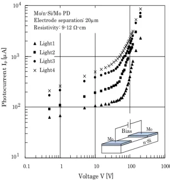
Figure 3 shows the typical photocurrent versus relations at room temperature under different illumination levels from a halogen lamp. Here the photocurrent component was obtained by subtracting the current under dark from the device current at each corresponding bias voltage. Each plot seems to be divided into two regions: the gradually increasing and rapidly increasing regions with bias. Since the present sample has the electrodes widely separated to avoid electronic interference between two junctions, the lateral separated in the depleted region would be more efficient to contribute to the photocurrent than the carriers optically generated in the residual undepleted neutral region. This would be the reason why the total photocurrent shows gradual increase with bias. The other region showing rapid increase in the photocurrent above about 12V seems to be under the onset of avalanche breakdown of the Schottky-junction reversed-biased, where the junction on the other side is, of course, forward-biased and it band structure is almost flattened.
It has generally been accepted that, for a semiconductor junction, the breakdown characteristic at voltages smaller than 6Eg qare attributed to the tunneling, where Egis the band-gap of the semiconductor considered and q is the elementary charge [3].
0.1 1 10 100 1000
Voltage V [V]
P
h
ot
oc
u
rr
e
n
t I
p
[
μ
A]
Mo/n-Si/Mo PD
Electrode separation: 20μm Resistivity: 9-12 Ω-cm
Light1 Light2 Light3 Light4
101 102 103 104
Bias
n-Si
Mo
Mo
Fig. 3. Photocurrent-voltage characteristics of a Mo/n-Si/Mo structure having 20μm electrode separation.
Incase of silicon at room temperature, 6Eg qis estimated
to be about 6.7 V. Therefore, the second region (larger than 30V) showing rapid increase might be the reflection of the onset of avalanche multiplication of carriers [4]. To confirm the idea above, we performed current-voltage characteristics measurements of this sample at different temperature. The result showed that the build-up voltage increases with temperature, that is, the temperature coefficient of build-up voltage is positive 2 o
[1.28 10 V/ C]× − .
10-04
10-03
10-02
10-01
1.0 10 102
103
0.1 1 10 100 1000
Voltage V [V]
Cu
rr
en
t[
u
A
]
T=300K T=99K T=77K
Mo/n-Si/Mo PD
Electrode separation : 20μm
Resistivity : 9-12 Ω-cm
Fig. 4. Photocurrent-voltage characteristics at different temperature which temperature coefficient is positive 2 o
[1.28 10 V/ C]× − .
Figure 4 shows the I-V characteristics of Mo/n-Si/Mo under in the dark conditions at different temperature. This charge in build-up voltage suggests that the avalanche breakdown process is sustainable in this structure [5].
As is well known, the avalanche process is inherently noisy process coming from stochastic ionization of carriers in high field [6]. To more clarify the onset and sustaining of avalanching, we also carried out shot noise measurements at frequencies 10-50 kHz. The noise measurements were performed using the system pictured in Figure 5(a). The noise to be detected was introduced into a 2kΩ load resistor series-connected with the device under test, the voltage drop across the load was then introduced to a low-noise
preamplifier and finally detected by a lock-in voltmeter. To check the system characteristic, a white noise generator was used. To irradiate the device, a xenon lamp dc-operated was used as a light source, the intensity of which was controlled by an ND filter.
ND
FILTER SW
ACOUSTO-OPTIC MODULATOR
SIGNAL GENERATOR
DC POWER SUPPLY SAMPLE
UNDER TEST OSCILLOSCOPE
FFT ANALYZER
He-Ne LASER λ : 633 nm
SW.1 SW.2
XENON LAMP
SAMPLE UNDER TEST ATTENUATOR
LOW NOISE PRE-AMP
OSCILLOSCOPE LOCK-IN VOLTMETER
DC POWER SUPPLY WHITE NOISE
GENERATOR
(a)
(b)
Fig. 5.
(a) Block diagram of noise measurement system. For calibration of the system and noise observation in time domain, sw.1 and sw.2 are switched, respectively. (b) Schematic diagram of the setup for photoresponse
measurements.
Proceedings of the International MultiConference of Engineers and Computer Scientists 2009 Vol II IMECS 2009, March 18 - 20, 2009, Hong Kong
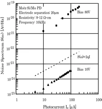
Figure 6 shows the 10kHz current noise versus photocurrent relationship on log-log scale at two biases 10V and 80V, where dashed line indicates full shot noise, the corresponding noise factor is unity. At low frequencies where the noise is independent of the frequencies, the current noise spectral density associated with the average current I is usually formulated as already given in Eq.(1).
2 2
( ) 2 (A /Hz) [1]
Sω = qIΓ
whereΓ2is the noise ratio or the noise factor representing
the ratio of the noise to full shot noise. One finds that the noise at 10V is proportional to the photocurrent, showing the noise is sub-shot noise and thus the noise factor of which is smaller than unity 2
[Γ <1]. Incase of the bias of 80V, however, proportionality relation still holds up its level becomes much higher than the full shot noise observed originates from the avalanche multiplication of the photocurrent [7].
10-25
10-24
1 10 100 1000
Photocurrent Ip[μA]
N
o
is
e
Sp
ec
tr
u
m
S(
ω
) [
A
2/H
z
]
Bias 10V Bias 80V
S(ω)=2qI
10-23
10-22
10-21
10-20
10-19
Mo/n-Si/Mo PD
Electrode separation: 20μm
Resistivity: 9-12 Ω-cm
Frequency: 10kHz
Fig. 6.Noise spectral density at 10 kHz versus photocurrent of Mo/n-Si/Mo structure, taking the bias voltage as a parameter.
The purpose of this section is to present the influence of operating condition on applied bias at the low frequency (50kHz) photoelectric response of planar Mo/n-Si/Mo structure with long neutral region. Optical response was measured using sinusoidal modulated He-Ne laser signal via an acousto-optic modulator (AOM). Figure 5(b) shows the block diagram for measurements of ac characteristics. An ND filter was used to control the light intensity and thus the photocurrent of the device.
The signal to be detected was fed to a load of 2 kΩ connected in series with the device under test. Then, the voltage drop across the load was conducted to an oscilloscope to observe instantaneous demodulated signals or to a Fast Fourier Transform (FFT) spectrum analyzer to view the signals received in frequency domain at biases 10 V to 30V as shown in Figure 7.
10 100
0.1 1
Ma
g
n
it
u
d
e
o
f
s
ig
n
a
l
[m
V
]
Voltage V [V]
200 Mo/n-Si/Mo PD
Electrode separation: 20μm
Resistivity: 9-12 Ω-cm
Frequency: 50kHz
Fig. 7. Spectra of the demodulated signals at biases V=10V to 180V(b) at 50 kHz for the same device in frequency domain by an FFT spectrum analyzer.
It was found that before breakdown (10-30V) the magnitude of output signal is dependence of applied bias. When the bias is towards near breakdown voltage (30-180V), the level of output signal much higher level is due to avalanche multiplication at high fields or hole injection from the anode. Because of the carrier multiplication due to impact ionization, the current entering the depletion layer is multiplied by factor, M, known as the multiplication factor, as it crosses the layer.
10 20 30 40 50 60 70 80 90 100
0
Frequency[kHz]
Ma
g
n
it
u
d
e
[
mV
]
0 40 80 120 160 200 240 280 320 360 400
Ma
g
n
it
u
d
e[
m
V
]
Frequency[kHz] 20μs
2 [
m
V
]
20μs
(a) Bias=10V (b) Bias=80V
Magnitude=29.05 μV Bias voltage=10V
0 40 80 120 160 200 240 280 320 360 400
10 20 30 40 50 60 70 80 90 100
0
Magnitude=289.7 μV Bias voltage=80V
10 [
m
V
]
Peak-to-peak=20mV Bias voltage=80V Peak-to-peak=2mV
Bias voltage=10V
(c) Bias=10V (d) Bias=80V
Fig. 8. Detected signal waveform at 50kHz under 10V pre-breakdown (a) and 80 V post-breakdown (b) conditions. (c) and (d) are the detected signals in frequency domain corresponding to biases in (a) and (b), respectively.
Proceedings of the International MultiConference of Engineers and Computer Scientists 2009 Vol II IMECS 2009, March 18 - 20, 2009, Hong Kong
Optical signal sinusoidal intensity-modulated was detected by the structures under pre-breakdown and post-breakdown regions. Figure 8(a) and (b) show the typical oscilloscope traces of the output signal versus bias voltage characteristics at frequency 50 kHz detected at two biases, 10Vand 80V, respectively. In this figure the amplitude of the demodulated waveform increases from 2.0mV (peak-to-peak) at a bias V=10V to 20mV at V=80V apparently showing the bias controlled iris effect is occurring.
Apparently the amplitude observed under breakdown condition (bias: 80V) is approximately one decade (40dB) larger than that below the breakdown voltage (bias: 10V). Even at 50kHz, 30dB gain was obtained. Figure 8 (c) and (d) show the frequency spectra of the detected signals under pre-breakdown and post-breakdown conditions corresponding to (a) and (b), respectively. Although that the increase in amplitude by the avalanche multiplication is observed, the width of the spectrum remains substantially unchanged at this frequency. Furthermore, the narrow line spectrum is obtained at two biases and thus no spurious effect was introduced in the demodulating process of the signal in time domain.
V. CONCLUSION
In conclusion, we observed dc photocurrent gain properties in silicon-based planar Mo/n-Si/Mo (MSM) structures. It was confirmed from the measurement of photocurrent versus voltage characteristics that an appreciable photocurrent enhancement was achieved. The rapid increase in photocurrent at higher biases is attributed to the effect of avalanche multiplication. Low frequency noise measurement was consistent with such avalanche multiplication.
ACKNOWLEDGMENT
The authors would like to express their sincere thanks to Dr.S.Supadech of King Mongkut’s Institute of Technology Ladkrabang for keen reading the manuscript and to Dr.F.Shishido of Kanagawa Institute of Technology for fruitful discussion. The authors are also thankful to T.Aoki of Tokai University for technical assistance throughout this work.
REFERENCES
[1] C. S. Harder, B. J. Van Zeghbroeck, M. P. Kesler, H. P. Meier, P. Vettiger, D. J. Webb, P. Wolf “High-speed GaAs/AlGaAs
optoelectronic devices for computer applications”, IBM J.Res.Develop, High-speed semiconductor devices, Vol.34, 1990, pp. 568-584.
[2] K. Sato and Y. Yasumura “Study of forward I-V plot for Schottky diodes with high series resistance”, J.App.Phys, Nov. 1, 1985,Vol. 58, Issue 9, pp. 3655-3657.
[3] S.M Sze, “Physics of Semiconductor Devices, 2nd ed. John-Wiely, New York, 1981.
[4] H. Melchior and W.T. Lynch, “Signal and. Noise Response of High Speed Germanium Avalanche Photodiodes,” IEEE. Trans. Electron Devices, vol. ED-13, Dec. 1966, pp. 829-838.
[5] A. Goetzberger, B. McDonald, R. H. Haitz, and R. M. Scarlett “Avalanche Effects in Silicon p—n Junctions. II. Structurally Perfect Junctions”, J. Appl. Phys. 34, 1963, pp. 1581
[6] R.J. McINTRYRE “Multiplication Noise in Uniform Avalanche Diodes”, IEEE. Trans. Electron Devices, vol. ED-13, Dec. 1966, pp. 164-168.
[7] T. Igo and K. Sato “Noise Characteristics in Silicon Photodiodes”, Jpn. J. Appl. Phys, Dec.1969, No. 12, Vol. 8 , pp.1481-1491.
Proceedings of the International MultiConference of Engineers and Computer Scientists 2009 Vol II IMECS 2009, March 18 - 20, 2009, Hong Kong