*e-mail: [email protected]
1. Introduction
In the last two decades, research directed at obtaining and characterizing nanometric coatings has been one of the most attractive subjects in the area of the science and engineering of surfaces. One of the applications that has been developed in the electrical sector especially is porcelain electrical insulators that are used in electrical energy transmission and distribution networks1-3.
An electrical insulator is a device used to guarantee the insulation of energized wires or cables from their adjacent support points. A premise of the functionality of these devices, which are made with materials of elevated mechanical strength and electrical resistance, is the ability to oppose the passage of an electrical current4.
The insulation used in high-power electrical networks can be made primarily using materials such as glass, polymeric materials or porcelain4. Porcelain is widely used in transmission and distribution networks.
Structurally, porcelain insulators consist of a dense body with an elevated dielectric rigidity and a glassy isolating layer coating, whose primary objective is to eliminate the surface porosity of the ceramic body to prevent trapping of water inside the pores. Even with the glassy coating, however, the accumulation of dirt on its surfaces can lead
to surface electrical conduction (leakage current) and a dielectric breakdown to the ground. This process generates heat and its magnitude depends on the nature of the adhered material, given that the predominance of the contaminating elements on the insulator will depend on the region in which it is located5-7.
The practical procedure currently performed to eliminate these surface pollutants is mechanical washing with water jets. However, this technique is not highly eficient because it is highly dependent on the insulator’s design and in addition requires special care regarding safety issues. Furthermore, it must be performed periodically7.
As a technical, scientiic and economically viable alternative, this study involves the development of nanometric ilms with hydrophobic and anti-adherent characteristics deposited by cold plasma on the surface of porcelain insulators from a titanium target. Materials with hydrophobic properties minimize leakage current, reducing surface wettability and promoting the low of water in which contaminating and conducting particles are carried.
Surfaces that repel water particles are designated as hydrophobic and occupy an important position in surface treatments8. Wettability is a property for the analysis of hydrophobicity. It is associated with the tendency of a liquid to
Nanostructured Titanium Film Deposited by Pulsed Plasma Magnetron Sputtering (Pdms)
on a High Voltage Ceramic Insulator for Outdoor Use
Kleber Franke Portellaa,b*, Priscilla Mengardab, Mariana d’Orey Gaivão Portella Bragançaa,
Sebastião Ribeiro Júniora, Jose Sergio Santos de Meloc, Dailton Pedreira Cerqueirac,
Sidnei Antonio Pianarod, Maurício Marlon Mazurb
aInstituto de Tecnologia para o Desenvolvimento, Institutos Lactec, Centro Politécnico,
Universidade Federal do Paraná – UFPR, Rodovia BR-116, Km 98, 8813, Jardim das Américas, CEP 81531-980, Curitiba, PR, Brazil
bUniversidade Federal do Paraná – UFPR, Av. Cel. Francisco H. dos Santos, 100,
Jardim das Américas, CEP 81531-980, Curitiba, PR, Brazil
cCompanhia de Eletricidade do Estado da Bahia – COELBA, Av. Edgar Santos, 300,
Cabula VI, CEP 41181-900, Salvador, BA, Brazil
dUniversidade Estadual de Ponta Grossa – UEPG, Av. Carlos Cavalcanti nº 4748,
Uvaranas, CEP 84030-900, Ponta Grossa, PR, Brazil
Received: June 22, 2015; Revised: August 10, 2015
In this study, the cold plasma technique was used to produce nanometric titanium ilms with hydrophobic and anti-fouling properties. The ilms where deposited on porcelain electrical insulators surfaces to minimize the effects of leakage current. The magnetron sputtering technique was used with a target of pure titanium sheet, and argon as the ionization gas. The deposited ilms present an average thickness of 58 to 350 nm. After coating the insulators, the assays performed indicated a greater degree of hydrophobicity and maintenance of leakage current after exposure to salt spray. Lower leakage current values were observed in both natural and saline environments compared with the uncoated device.
Portella et al.
854 Materials Research
spread on a surface and is characterized by a parameter called the contact angle (θ). This angle corresponds to the extent to which water can spread on a surface9-11. Materials with a
contact angle less than 45° are classiied as hydrophilic, and materials with angles greater than 45° are hydrophobic12,13.
Another characteristic related to surface wettability is the self-cleaning effect, which can be explained by contact angle hysteresis and low adhesion. When hysteresis is low, the drop tends to roll on the surface and carry the particles. For droplets that have kinetic energy, such as raindrops, hydrophobic surfaces are easily cleaned14.
Hydrophobic coatings favor the formation of droplets on their surface in which dust particles and impurities tend to adhere, favoring their cleaning. These coatings are normally used on glass surfaces in nanometric dimensions to reduce the liquid surface tension15.
The insulator surface glassy layer shows chemical heterogeneity due to its composition and open chemical bonds on its surface. These bonds are Si-O- and Si- type with other elements. When the glass enters into contact with the atmosphere, OH- groups are adhered to it, and a lower energy and greater stability is obtained. This adhesion makes the surfaces prone to showing a hydrophilic character16.
Various organic and inorganic materials have been studied with the objective of altering the properties of glassy surfaces. Polymers such as acrylic, polyester, polyurethane, and silicon are among the organic materials that have been tested as electrical insulator coating with a hydrophobic functionality. However, some limitations are still observed in these types of materials such as degradation by electrical tracking and erosion that can cause failures and limit the materials useful lifespan17.
Metallic materials, especially titanium, deposited under speciic conditions in which the chemical and structural nature of the substrate must be analyzed, can also be used for the surface recombination of glassy layers (Ti-O-Si). Such coatings can alter the wetting properties of the surface formed once the OH- groupings are substituted. Additionally,
titanium ilms have high mechanical strength, excellent thermal stability and good corrosion resistance in highly aggressive environments18-20.
In processes that involve cold plasmas, some determining factors must be deined: the energy source, feed system and the choice of the precursor gases, reactor type and the types of substrates, with the latter and the geometric factors related to the surroundings of the plasma phase being crucial to the eficiency of these processes21. In cold plasma whose gas is
conined in a controlled environment under pressures on the order of 10–3 Pa, to guarantee greater ionization eficiency for the species, energy sources such as luminescent discharges of direct current and radiofrequency discharges are widely used22,23.
One of the processes used for the deposition of nanometric ilms on substrates is sputtering, which promotes the disarrangement and removal of atoms from the surface of the material (target) for deposition on another (substrate)24.
In the majority of cases that involve deposition by sputtering, a magnetron is coupled that consists of magnets close to the target that promote the accumulation of electrical charges and favor greater bombardment of the species in
the region. Through this process, high-quality, thicker, and uniform ilms can be produced when the application requires these characteristics, such as in the coating industry, in which the ilm formed requires high resistance to wear, weathering and corrosion25-28.
2. Experimental Design
2.1. The substrate preparation
A ceramic insulator of commercial porcelain measuring 132.8 mm in height with a base 182.6 mm in diameter was used as the substrate (Figure 1a). Deposition on the insulator was performed in four steps: irst upon the face shown in Figure 1b. Then, another with the sample turned 90°. The third deposition on the face shown in Figure 1c, and again one with this face turned 90°. In each step the vacuum was broken with the injection of argon.
The insulator was prepared initially by washing with water and detergent, followed by cleaning with acetone (PA) and isopropyl alcohol (PA). Drying was performed in an oven at 100 °C for one hour. After drying, the substrate was placed in the center of the plasma reactor.
2.2. Cold plasma reactor and deposition
parameters
The deposition equipment schematic drawing is shown in Figure 1d. The monitoring system consists of a programmable logic controller whose monitors are actuated when there is a failure in the refrigeration of the diffusion pump or in the absence of the magnetron refrigeration system. From this set up, pressures about 0.13 Pa can be achieved using the mechanical pump, and pressures up to 1.3×10⁻³ Pa can be achieved using a diffusion pump. The vacuum system also serves to close the chamber. In the system, the working gas inlet (in this study, argon 99.999% purity), was controlled by valves that were also present in the chamber. The structure of the reactor was made of aluminum, and the plasma was conined in borosilicate glass supported by stainless steel. Inside the reactor, a cathode was developed containing a balanced magnetron with a hollow body made of copper through which cooling water circulated. A 99.999% purity planar titanium target was placed in the cathode with dimensions of 80 × 245 mm. The entire internal region of the chamber consisted of the anode. The feed system consisted of a direct current source, with a voltage signal modulated by a pulse width. A frequency source of 25 kHz with 30% duty cycle was employed. The inal working current was 1.2 A. The source power during deposition was 0.65 KW.
In each step, the inal pressure obtained after generation of the vacuum was 5.5 × 10⁻³ Pa, and the working pressure after the insertion of argon gas was 0.82 Pa. The deposition time was 20 s after activating the energy source.
2.3. Characterization of the material
For the analysis of the ilm’s roughness and thickness, the samples were subjected to atomic force microscopy (AFM) in contact mode using an SPM-9600 microscope from Shimadzu.
Hydrophobicity was evaluated in samples from the insulator using the contact angle and pulverization methods12,13. The leakage current test of insulators with and without deposition was also performed before and after being subjected to artiicial salt spray weathering for alternating current systems with nominal voltages higher than 1000 V13-29.
3. Results and Discussion
3.1. Characterization by SEM/FEG and AFM
Two different regions of the coated substrate cross-section were examined with SEM/FEG, as shown in Figure 2a and Figure 2b, with ilm average thickness of 58 and 350 nm, respectively. The comparison of these regions demonstratesan irregularity in the deposition; it is due to the distance between the different substrate sections and the titanium target.
The elemental analysis measurement (EDS) was performed on the sample of Figure 2b, in the region of substrate and deposited ilm (analysis 1 and 2, respectively). The EDS spectra and quantitative analysis are indicated in Figure 2c and Figure 2d.
The element titanium was identiied, corroborating the deposited ilm. Additionally, the presence of the elements silicon, aluminum, and oxygen was veriied; their presence was attributed to the silicates and aluminates present in the glass that covered the porcelain30.
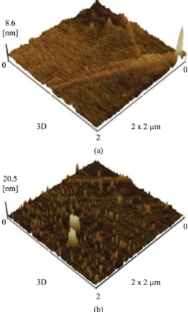
Atomic force microscopy (AFM) was performed on the samples before and after the ilm deposition. Figure 3a shows a three-dimensional image of the original surface, showing its irregularities descendant from the fabrication process. Figure 3b shows the three-dimensional aspect of the deposited ilm, indicating a complete change on its aspect,
Portella et al.
856 Materials Research
when compared to the original substrate. The presence of small peaks throughout the sample surface indicate that the deposited ilm was not continuous. This can be related to a nucleation process that occurred at isolated areas on the substrate during the deposition time of 20 seconds. Regarding the average roughness (Rx), the uncoated material showed a value of 0.6 nm, and the coated material showed 1.2 nm. Although the Rx value for the insulator with deposition was double the value for the uncoated insulator, this parameter may not be suficiently expressive for the analysis because the glass of the sample itself had an irregular surface.
3.2. Hydrophobicity - contact angle method and
sprayer method
The sample without deposition (Figure 4a) had a contact angle of 38.2°. The sample with the nanometric titanium ilm (Figure 4b) had a contact angle of 73.4°. The irst surface was classiied as hydrophilic (angle less than 45°), and the second one was classiied as hydrophobic (angle between 45° and 90°)12,13.
Regarding the hydrophobicity analysis using the sprayer method, the insulator without ilm deposition was classiied as CM4, and the other insulator was classiied as CM3. The angle calculated for this classiication was that of the indentation, which was evaluated as being between 0° and 50°. This result signiies that the insulator with the nanometric coating showed greater hydrophobicity because the classiication goes from CM1 (most hydrophobic) to CM7 (most hydrophilic)12,13.
Figure 2. (a, b) Deposited ilm cross section SEM/FEG images, deposited on the insulator surface. (c, d) Elemental chemical analysis by EDS.
Figure 3. Three-dimensional AFM images in contact mode.
3.3. Leakage current test
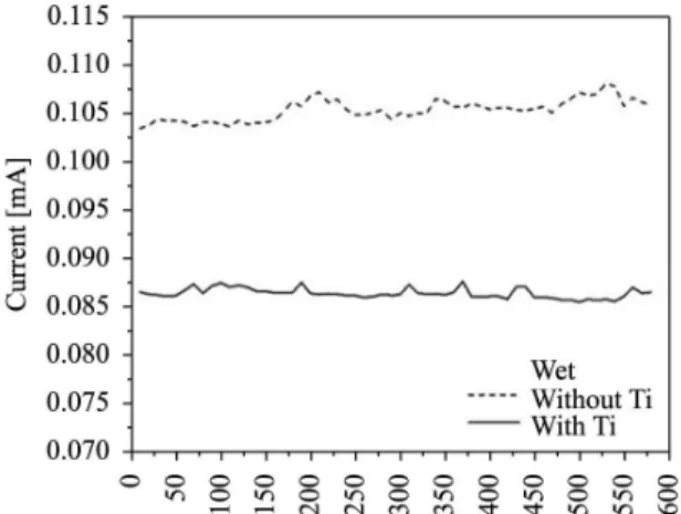
The results for leakage current are shown in Figure 5 (maximum current obtained relative to the time of exposure to artiicial weathering) in the insulators with and without deposition of a nanometric titanium ilm, before (a) and after the salt spray test (b). The insulator with the nanometric ilm with and without exposure to accelerated weathering showed lower leakage current values over time when compared with the insulator without deposition (regardless of exposure to the salt spray).
The results indicate that the hydrophobicity achieved by the deposition of nanometric titanium ilms using cold plasma contributed to the minimization of the leakage current on the surface of the insulator over time. This evidence is highlighted in Figure 6. In the salt spray exposure condition, the insulator with deposition showed an average decrease in current of 8.4% compared with the insulator without deposition.This degree of decrease is signiicant in high- and medium- voltage electrical networks.
The variation in the comparison of the leakage current between the insulators before and after exposure to artiicial weathering was more tenuous for the coated material. This result was attributed to the fact that, even when exposed to an environment that could favor surface electrical conduction, the modiied material had lower current values, and the ilm formed showed suficient hydrophobicity to promote a self-cleaning effect to repel the saline particles from its surface.
Figure 6. Comparison of the maximum leakage current obtained during the salt spray test on the insulators with and without
nanometric ilm deposition.
4. Conclusion
Nanometric ilms were deposited on glass surfaces of high-electrical-voltage porcelain insulators from a titanium target by sputtering in cold plasma. The results indicated characteristics of increased hydrophobicity and chemical resistance to weathering by chlorides with a reduction of leakage current, even on wetted surfaces.
Figure 4. Image of the insulator sample for calculating the contact angle by the addition of a water droplet on the surface using a goniometer. (a) Sample without deposition. (b) Sample with deposition.
Figure 5. (a) Maximum leakage current obtained on an insulator without deposition before and after accelerated aging; and (b) on
an insulator with nanometric ilm deposition before and after
Portella et al.
858 Materials Research
Acknowledgements
The authors thank the LACTEC Institutes, the Electrical Company of the State of Bahia (Companhia de Eletricidade do Estado da Bahia (COELBA)) and the Brazilian National Agency of Electrical Energy (Agência Nacional de Energia
Elétrica (ANEEL)), P&D 0047-0047/2011, and CNPq/Lei 8010/90 and CNPq/PIBITI, for their contribution in this project. We also thank the Multiusers Laboratory of the State University of Ponta Grossa for performing the FEG, FTIR and AFM measurements.
References
1. Averback RS, Höfler HJ, Hahn H and Logas JC. Sintering and grain growth in nanocrystalline ceramics. Nanostructured Materials. 1992; 1(2):173-178. http://dx.doi.org/10.1016/0965-9773(92)90072-6.
2. Rao CNR, Muller A and Cheetham AK. Nanomaterials Chemistry recent developments and new directions. 1st ed. Weinheim: Wiley-VCH; 2007.
3. Brechignac CP and Lahmani HM. Nanomaterials and nanochemistry. New York: Springer; 2006.
4. Saraiva DB. Isolantes e dielétricos. In: Saraiva DB, editor. Materiais elétricos. Rio de Janeiro: Guanabara Koogan; 1988. p. 98-107.
5. Su H, Jia Z, Guan Z and Li L. Mechanism of contaminant accumulation and flashover of insulator in heavily polluted coastal area. IEEE Transactions on Dielectrics and Electrical Insulation. 2010; 17(5):1635-1641.
6. Reddy BS and Nagabhushana GR. Study of temperature distribution along an artificially polluted insulator string. Plasma Science and Technology. 2003; 2(2):1715-1720. http://dx.doi. org/10.1088/1009-0630/5/2/006.
7. Portella KF, Piazza F, Cabussú MS, Inone PC, Cerqueira DP and Chaves CS. Estudo dos efeitos da poluição atmosférica em isoladores de distribuição e métodos alternativos para minimizá-los [Relatório Final de Projeto LACTEC/COELBA]. Curitiba: Institutos Lactec; 2007.
8. Yao L and He J. Recent progress in antireflection and self-cleaning technology – from surface engineering to functional surfaces. Progress in Materials Science. 2014; 61:94-143. http://dx.doi.org/10.1016/j.pmatsci.2013.12.003.
9. Koch K and Barthlott W. Superhydrophobic and superhydrophilic plant surfaces: an inspiration for biomimetic materials. Philosophical Transactions of the Royal Society of London. Series A, Mathematical and Physical Sciences. 2009; 367(1893):1487-1509. http://dx.doi.org/10.1098/rsta.2009.0022. PMid:19324720.
10. Gennes P, Brochard-Wyard F and Quéré D. Capillarity and wetting phenomena: drops, bubbles, pearls, waves. New York: Springer-Verlag; 2003.
11. Roach P, Shirtcliffe N and Newton MI. Progress in superhydrophobic surface development. Soft Matter. 2008; 4(2):224-240. http:// dx.doi.org/10.1039/B712575P.
12. Shaowu W, Xidong L, Zhicheng G, Jun Y and Qinghe S. Investigation on hydrophobicity and pollution status of composite insulators in contaminated areas.In: Annual Report Conference on Electrical Insulation and Dielectric Phenomena; 2001; Kitchener, Ontario. Kitchener: IEEE; 2001. p. 628-631.
13. Gao H, Jia Z, Guan Z, Mao Y, Wang L and Zhu K. Evaluation of electrical insulator proprieties on aged composite insulator in heavily contaminated areas. In: Conference Record. International Symposium on Quality Electronic Design; 2006; Toronto, Ontario. Toronto: IEEE; 2006. p. 197-200.
14. Lai Y-K, Chen Z and Lin C-J. Recent progress on the superhydrophobic surfaces with special adhesion: from natural to biomimetic to functional. Journal of Nanoengineering and
Nanomanufacturing. 2011; 1(1):18-34. http://dx.doi.org/10.1166/ jnan.2011.1007.
15. Berto AM. Revestimentos cerâmicos: acima e além das aplicações tradicionais. Cerâmica Industrial. 2008; 13:7-12.
16. Doremus RH. Glass Science. New Jersey: John Wiley& Sons; 1994.
17. Meyer LH, Jayaram SH and Cherney EA. A novel technique to evaluate the erosion resistance of silicone rubber composites for high voltage outdoor insulation using infrared laser erosion. In: Proceedings of the 12th IEEE International Symposium on Quality Electronic Design; 2005; Santa Clara, USA. Santa Clara: IEEE; 2005. p. 1201-1208.
18. Zhang L, Shi LQ, He ZJ, Zhang B, Lu YF, Liu A et al. Deposition of dense and smooth Ti films using ECR plasma-assisted magnetron sputtering. Surface and Coating Technology. 2009; 203(22):3356-3360.
19. Jeyachandran YL, Karunagaran B, Narayandass SK, Mangalaraj D, Jenkins TE and Martin PJ. Properties of titanium films deposited by dc magnetron sputtering. Materials Science and Engineering A. 2006; 431(1-2):277-284. http://dx.doi. org/10.1016/j.msea.2006.06.020.
20. Mahmoud S. Structure and optical properties of thin titanium films deposited on different substrates. Journal of Materials Science. 1987; 22(10):3693-3697. http://dx.doi.org/10.1007/ BF01161479.
21. Cho DL and Yasuda H. Influence of geometric factors of the substrate on hydrophilic surface modification of polyurethane sponges by plasma treatment. Journal of Vacuum Science & Technology. A, Vacuum, Surfaces, and Films. 1986; 4(5):2307-2316. http://dx.doi.org/10.1116/1.574068.
22. Conrads H and Schmidt M. Plasma generation and plasma sources. Plasma Sources Science & Technology. 2000; 9(4):441-454. http://dx.doi.org/10.1088/0963-0252/9/4/301.
23. Bogaerts A, Neyts E, Gijbels R and Van der Mullen J. Gas discharge plasmas and their application. Spectrochimica Acta Part B. Acta5. 2002; 57(4):609-658. http://dx.doi.org/10.1016/ S0584-8547(01)00406-2.
24. Ait Djafer AZ, Saoula N, Madaoui N and Zerizer A. Deposition and characterization of titanium carbide thin films by magnetron sputtering using Ti and TiC targets. Applied Surface Science. 2014; 312:57-62. http://dx.doi.org/10.1016/j.apsusc.2014.05.084.
25. Kelly PJ and Arnell RD. Magnetron sputtering: a review of recent developments and applications. Vacuum. 2000; 56(3):159-172. http://dx.doi.org/10.1016/S0042-207X(99)00189-X.
26. Karthikeyan S, Hill AE, Cowpe JS and Pilkington RD. The influence of operating parameters on pulsed D.C. magnetron sputtering plasma. Vacuum. 2010; 85(5):634-638. http://dx.doi. org/10.1016/j.vacuum.2010.09.007.
28. Bulír J, Novotný M, Lancok J and Fekete L. Nucleation of ultrathin silver layer by magnetron sputtering in Ar/N2 plasma. Surface and coating technology. 2013; 228(Suppl 1):586-590.
29. Muncivi A, Sarkar P and Haddad A. Tracking wheel test facilities.
In: Proceedings of the 44th International Universities Power
Engineering Conference; 2009; Glasgow. Glasgow: IEEE; 2009. p. 1-5.