Ricardo Caranicola Caleffo
Department of Electronic Systems Engineering Polytechnic School, University of São Paulo (USP)
Av. Prof. Luciano Gualberto, Trav. 3, nº 380, SP - São Paulo, Brazil [email protected]
Abstract— Normally the physical dimensions of the taper transition
that realizes the impedance matching between the impedance of the feeding line built in microstrip line technology and the impedance of the component built in Substrate Integrated Waveguide (SIW) technology are obtained by computational optimization processes due the difficulty of analytical treatment. This research work presents a new empirical approach to determine all the physical dimensions of this particular planar transition without using any computational optimization process. The well-defined design procedure is based on an approximation according with electromagnetic simulations and electromagnetic theory. The main goal is to facilitate the integration between SIW technology and planar circuits. The whole design procedure considers central frequency for the recommended bandwidth in the TE10 propagation
mode and power-voltage impedance definition for the SIW. Two structures are designed on RT/duroid 5880 to operate in the X band and Ku band, and the frequency response for both structures are compared by electromagnetic simulation and experimental results. The structure operating in X Band demonstrated return loss better than 10.0 dB at 61.67% of the considered bandwidth and the structure operating in Ku Band demonstrated return loss better than 10.0 dB at 72.88% of the considered bandwidth.
Index Terms— Planar circuits, SIW technology, Taper transitions. I. INTRODUCTION
Rectangular Waveguides (RWG) are widely applied in the microwave frequencies due a low power
dissipation and high quality factor. In contrast, shows as disadvantage a high fabrication cost and the
integration with planar circuits require sophisticated transitions. To avoid these problems, has been
proposed a structure called Substrate Integrated Waveguide (SIW). The components built using SIW
technology are designed and fabricated on a planar dielectric substrate low losses and having
periodical metalized vias that replaces the side walls of the traditional RWG, confining the
electromagnetic wave inside the dielectric substrate, allowing in this way an easy integration with
planar circuits [1]. The SIW technology can be employed in applications to operate since the S band
until Ka band. The frequency limitation in SIW technology occurs due the dielectric loss affects
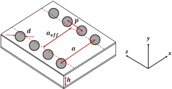
strongly the electromagnetic wave propagation. Fig. 1 shows a generic SIW.
Fig. 1. Generic substrate integrated waveguide.
Where is the effective width, ℎ is the dielectric substrate thickness, is the diameter of
metalized vias, is the periodical spacing between two consecutives metalized vias, and is the
spacing between the two rows of metalized vias. Due the side walls are replaced by metalized vias,
the longitudinal electrical current is not allowed, so the SIW support just the TE propagation mode
[1], [2]. The absence of TM propagation mode creates a favorable condition for design bandpass
filters [1], [3]. The electromagnetic waves propagation in SIW technology is affected by the insertion
of periodical metalized vias and some studies and analyses has been done for understanding the
operation of this technology [4], [5]. Due the difference of propagation modes and guided modes,
modeling of conductor, dielectric, and radiation losses in SIW technology is also a target of study [6].
The SIW technology can be applied in many applications, such as traditional structures of power
dividers/combiners [7] and dividers/combiners based on directional couplers [8], [9]. Normally the
components built in SIW technology are fed by a microstrip line with a characteristic impedance of
Ω and the integration between them can be made by a taper transition, such as [7]-[9]. The taper transition realizes the impedance matching between the impedance of the feeding line and the
impedance of the SIW component. Due the difficult of analytical treatment, computational
optimization processes has been widely used to determine the physical dimensions of this planar
transition. There are some studies that provide an appropriate treatment for analyze the taper transition
and some examples have been demonstrated [10], [11].
This research work presents a new empirical approach to determine all the physical dimensions of
the taper transition in an easy way without using any computational optimization process. The main
aim is to obtain return loss better than 10.0 dB and low insertion loss in the recommended bandwidth
for the SIW. The paper is organized according with the next description: Section II presents the main
design considerations for the SIW component and the main characteristics for the feeding line.
Section III presents the well-defined design procedure based on an approximation according with
electromagnetic simulations and electromagnetic theory to determine the physical dimensions of the
taper transition. Section IV presents two application examples using the design procedure established
in this paper in the X band and Ku band. Both application examples consider TE10 propagation mode
and are designed and fabricated on a RT/duroid 5880. Finally the Section V shows the main
II. DESIGN CONSIDERATIONS
An important design factor is know how the impedance of each element of the whole structure
operate as a function of frequency to realize the impedance matching between the impedance of the
feeding line and the impedance of the SIW component. The dielectric substrate loss is also an
important design factor and the � must be as low as possible. The dielectric substrate thickness
provides the height of the SIW component and the feeding line, being in this way, the only design
parameter that does not allow changes after the choice of the dielectric substrate.
A. Substrate Integrated Waveguide
The RWG concepts and theory can be directly applied in studies and projects involving SIW
technology. Generally the component built in SIW technology operates in TE10 mode and higher
modes are not considered due the undesirable electric field configuration. But is necessary knowing
the operation frequency of TE20 propagation mode to avoid the SIW component operates in this
particular propagation mode. The cutoff frequencies for the SIW are written as a function of the
effective widths [1].
� � = √��( � ) (1)
Where ≥ , is the relative dielectric constant, and is the speed of light. According with
[1], [2] the equations of the cutoff frequencies for the TE10 and TE20 propagation modes are given by
(2)-(3).
� � = √��( ) = √�� − . + .
−
(2)
� � = √��( ) =√�� − . + . .
−
(3)
The parameters , , and determine the effective widths for the TE10 and TE20 propagation
modes, which these determine the cutoff frequencies. The choice for these three parameters is not
random and depends on four rules for the SIW operate as a waveguide [1]. After determine the cutoff
frequencies for the TE10 and TE20 propagation modes, it is possible determine a bandwidth for the
component built in SIW technology. According with the recommended bandwidth for the RWG [12],
the recommended bandwidth for the SIW that guarantees the operation exactly in the TE10
propagation mode and low losses is given by (4).
. ∙ �
� < < . ∙ � � (4)
The central frequency of the recommended bandwidth given by (4) can be written by (5).
= . ∙� � � + .9 ∙� � � (5)
With the recommended bandwidth (4) and central frequency (5) obtained it is possible evaluate the
cross-section impedance of the SIW component in the TE10 propagation mode. The cross-section
This research work employs the power-voltage (P-V) impedance definition due the majority of
electromagnetic simulators using this impedance definition. The power-voltage (P-V) impedance
definition can be written by (6),
� �− = .
∗
� (6)
where � is the voltage drop between the top and the bottom metallic walls of the SIW component, �∗
is the conjugated of �, and � is the incident power at the cross-section of the SIW component given
by the Poynting theorem. For the TE10 propagation mode, the cross-section impedance can be written
according with the SIW physical dimensions in the same way as given by the RWG [1], [12],
� �− = ℎ √���[ − � ]
−
(7)
where ℎ is the dielectric substrate thickness, is the effective width for the TE10 propagation
mode, is the intrinsic impedance of the free space, is the relative dielectric constant of the
substrate, is the cutoff frequency, and is the operation frequency. At the central frequency of the
recommended bandwidth for TE10 propagation mode (5), the cross-section impedance of the SIW
component can be expressed by (8).
� �− = ℎ √���[ − . � � �
� � � + .9 � � � ]
−
(8)
B. Feeding line
The feeding line used in this work is built in microstrip line technology and has Ω of impedance
characteristic and it is designed at the central frequency of the recommended bandwidth by (5).
III. DESIGN PROCEDURE FOR TAPER TRANSITION
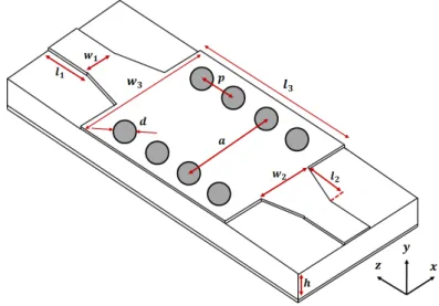
The Fig. 2 shows a symmetric structure used in this research work containing two microstrip lines
that feeds the whole structure with same physical dimensions, a substrate integrated waveguide, and
two taper transitions that realizes the impedance matching with same physical dimensions.
The taper transition in Fig. 2 is responsible to realize the impedance matching between the
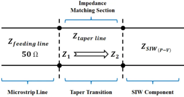
impedance of the feeding line and the impedance of the SIW component. The Fig. 3 shows a
schematic of impedance matching considered in this research work.
Fig. 3. Schematic of impedance matching between feeding line and SIW component.
The cross-section impedance between the feeding line and the taper transition is defined as
= Ω and the cross-section impedance between the taper transition and the SIW component is defined as . For a good impedance matching must be closest possible of � �− . The
impedance value is given by the microstrip line impedance [13], where the cross-section physical
dimensions are given by � and ℎ. For this work is valid the relation � /ℎ > .
= �
√� { �ℎ + . 9 + . ∙ [�ℎ + . ]} (9)
where is the effective dielectric constant for a microstrip line with physical dimensions � and ℎ
[13].
The physical dimension also makes a contribution for the impedance matching. According
with [14], the reflection coefficient for a triangular taper is a function of .
� = | [ � / � / ] | − � (10)
where � is the propagation constant of the tapered line [14].
In many cases, the taper transition physical dimensions are obtained by computational optimization
processes due the difficult of an analytical treatment. One of the factors that increase the difficulty of
analytical treatment is the difference of field configuration between SIW component and microstrip
line. The substrate integrated waveguide support just TE propagation mode [1], [2] and the microstrip
line technology in many practical applications has a quasi-TEM propagation mode [13].
According with Fig. 2, the taper transition physical dimensions are given by � , � , and , whence
the physical dimension � is given by the feeding line. Therefore, the physical dimensions � and
are the dimensions to be determined. In this section will be demonstrated a new empirical approach
for determine these two physical dimensions.
The taper transition is a microstrip line with variable width, beginning with a width � and
finishing with a width � , therefore, an effective dielectric constant value cannot be applied directly
This research work will approximate an effective dielectric constant value for the taper transition
and this respective approximated value has the same effective dielectric constant value of the feeding
line. This approximation considers the electromagnetic wave that is being propagated along the taper
transition has the same wavelength of the electromagnetic wave that is being propagated along the
feeding line. The proposed approximation is done due initially the only available physical dimension
for the taper transition is � , given by the feeding line width.
To justify this approximation was designed, optimized, and simulated 13 structures in six different
operation bands using the High Frequency Structure Simulator (HFSS). For each structure was
obtained a return loss better than 10.0 dB in the recommended bandwidth by (4). The main aim of the
3D computational electromagnetic simulations realized is to verify how much the difference between
the widths � and � affects the effective dielectric constant value and the impedance value.
Will be shown that a mean error lower than 6% is present when is taken a unique effective
dielectric constant value for the taper transition and feeding line, and a mean error lower than 7% is
present in the impedance matching between the taper transition and the SIW component considering
the proposed approximation.
The reference values used for the proposed approximation are √ and √ , where the first one
considers the width � and the second one considers the width � , and both of them have the same
dielectric substrate thickness (ℎ). The reason for considerer √ is due the wavelength calculation be
divided by this term and all the physical dimensions considered are a function of the wavelength.
A smaller difference between √ and √ provides a better approximation for a unique effective
dielectric constant value ( ), where √ it is the error reference for the proposed approximation. To
obtain the error for the proposed approximation (11) it is considered.
��� �(√ )%=|√� −√� |√� ∙ (11)
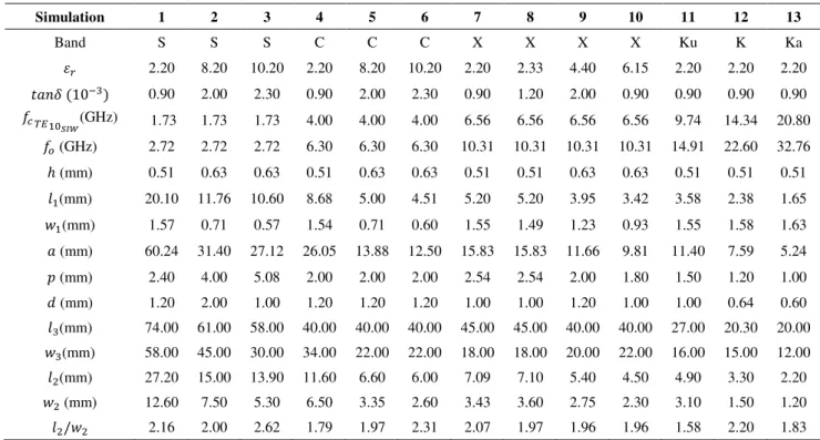
Table I shows the 13 structures designed and optimized covering since S band until Ka band, and
considers the bandwidth given by (4) and central frequency given by (5). The structures shown in
Table I have two different values of dielectric substrate thickness, 0.51 mm and 0.63 mm. The
substrate integrated waveguide and feeding lines physical dimensions were obtained according with
the design considerations presented in Section II. The taper transition physical dimensions � and
were obtained by computational optimization processes providing a return loss better than 10.0 dB
Table I. 13 structures designed and optimized covering since S band until Ka band.
Simulation 1 2 3 4 5 6 7 8 9 10 11 12 13
Band S S S C C C X X X X Ku K Ka
2.20 8.20 10.20 2.20 8.20 10.20 2.20 2.33 4.40 6.15 2.20 2.20 2.20
� − 0.90 2.00 2.30 0.90 2.00 2.30 0.90 1.20 2.00 0.90 0.90 0.90 0.90 � � (GHz) 1.73 1.73 1.73 4.00 4.00 4.00 6.56 6.56 6.56 6.56 9.74 14.34 20.80
(GHz) 2.72 2.72 2.72 6.30 6.30 6.30 10.31 10.31 10.31 10.31 14.91 22.60 32.76
ℎ (mm) 0.51 0.63 0.63 0.51 0.63 0.63 0.51 0.51 0.63 0.63 0.51 0.51 0.51 (mm) 20.10 11.76 10.60 8.68 5.00 4.51 5.20 5.20 3.95 3.42 3.58 2.38 1.65
� (mm) 1.57 0.71 0.57 1.54 0.71 0.60 1.55 1.49 1.23 0.93 1.55 1.58 1.63 (mm) 60.24 31.40 27.12 26.05 13.88 12.50 15.83 15.83 11.66 9.81 11.40 7.59 5.24
(mm) 2.40 4.00 5.08 2.00 2.00 2.00 2.54 2.54 2.00 1.80 1.50 1.20 1.00 (mm) 1.20 2.00 1.00 1.20 1.20 1.20 1.00 1.00 1.20 1.00 1.00 0.64 0.60 (mm) 74.00 61.00 58.00 40.00 40.00 40.00 45.00 45.00 40.00 40.00 27.00 20.30 20.00
� (mm) 58.00 45.00 30.00 34.00 22.00 22.00 18.00 18.00 20.00 22.00 16.00 15.00 12.00 (mm) 27.20 15.00 13.90 11.60 6.60 6.00 7.09 7.10 5.40 4.50 4.90 3.30 2.20
� (mm) 12.60 7.50 5.30 6.50 3.35 2.60 3.43 3.60 2.75 2.30 3.10 1.50 1.20
/� 2.16 2.00 2.62 1.79 1.97 2.31 2.07 1.97 1.96 1.96 1.58 2.20 1.83
According with Table I an arithmetic mean considering the 13 relations /� can be written.
� = ∑= (���)/ = . (12)
And an approximation can be written by (13) according with (12).
� = (13)
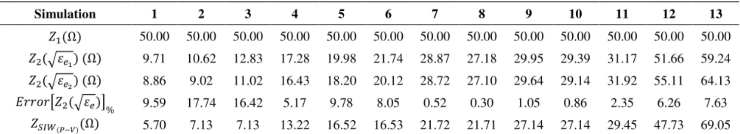
According with (8) and (9), the impedance values for the 13 structures are shown in Table II.
Table II. Impedance values for the 13 structures.
Simulation 1 2 3 4 5 6 7 8 9 10 11 12 13
Ω 50.00 50.00 50.00 50.00 50.00 50.00 50.00 50.00 50.00 50.00 50.00 50.00 50.00
Ω 8.86 9.02 11.02 16.43 18.20 20.12 28.72 27.10 29.64 29.14 31.92 55.11 64.13
� �− Ω 5.70 7.13 7.13 13.22 16.52 16.53 21.72 21.71 27.14 27.14 29.45 47.73 69.05
According with Table II the impedance values are tending to � �− impedance values,
demonstrating in this way, the impedance matching provided by the taper transition.
Table III shows the error for the proposed approximation in this research work considering the 13
designed and optimized structures. To obtain the value for was considered the physical dimensions
ℎ and � and for was considered the physical dimensions ℎ and � . The error considers (11).
Table III. Error for the proposed approximation in this research work considering the 13 designed and optimized structures.
Simulation 1 2 3 4 5 6 7 8 9 10 11 12 13
1.87 5.65 6.81 1.87 5.65 6.84 1.87 1.96 3.33 4.42 1.87 1.87 1.88 2.09 7.14 8.55 2.03 6.59 7.92 1.96 2.07 3.58 4.82 1.95 1.87 1.84
According with Table III an arithmetic mean for the error can be written conform (14).
��� �(√ )% = ∑ |√� �−√� �|
√� � ∙
= / = . % (14)
According with (14) a mean error lower than 6% is present in this proposed approximation
considering the 13 designed and optimized structures. Due the low mean error obtained, a unique
effective dielectric constant value is taken for the taper transition and feeding line ( ). Therefore, the
wavelength of an electromagnetic wave that is being propagated along the taper transition is
approximated to the wavelength of an electromagnetic wave that is propagated along the feeding line
with a mean error lower than 6%. The obtained error is related with 13 designed and optimized
structures in Table I.
Considering the proposed approximation, an impedance can be rewrite considering √ .
(√ ) =√� {� �
ℎ + . 9 + . ∙ [ �ℎ + . ]}
(15)
To evaluate the impact of the proposed approximation in the impedance matching between the taper
transition and the SIW component, a mean error can be obtained for the impedance matching. For the
error related with the impedance matching, the (√ ) impedance value is taken as reference.
��� �[ √ ]%=| (√� )− (√� )|(√� ) ∙ (16)
Table IV shows a comparison between √ and √ , the and � �− impedance
values are also considered. The main aim of this comparison shown in Table IV is to evaluate the
difference in the impedance matching when is considered a unique effective dielectric constant value.
Table IV. Impedance values for the 13 structures considering the proposed approximation and the error caused by it.
Simulation 1 2 3 4 5 6 7 8 9 10 11 12 13
Ω 50.00 50.00 50.00 50.00 50.00 50.00 50.00 50.00 50.00 50.00 50.00 50.00 50.00
√ Ω 9.71 10.62 12.83 17.28 19.98 21.74 28.87 27.18 29.95 29.39 31.17 51.66 59.24
√ Ω 8.86 9.02 11.02 16.43 18.20 20.12 28.72 27.10 29.64 29.14 31.92 55.11 64.13
��� �[ √ ]% 9.59 17.74 16.42 5.17 9.78 8.05 0.52 0.30 1.05 0.86 2.35 6.26 7.63
� �− Ω 5.70 7.13 7.13 13.22 16.52 16.53 21.72 21.71 27.14 27.14 29.45 47.73 69.05
According with Table IV, an arithmetic mean for the impedance matching error considering the 13
impedance values for √ and √ can be written by (17).
��� �[ √ ]% = ∑ | (√� )�− (√� )�|
(√� )� ∙
= / = . % (17)
According with (17), the proposed approximation affects less than 7% the impedance matching
between the taper transition and the SIW component.
Based on the proposed approximation, a wavelength of an electromagnetic wave being propagated
along the taper transition can be calculated considering central frequency at the recommended band
� (√ , ) = . ∙
� � + .9 ∙� � ∙√� (18)
Table V shows a comparison between the wavelength � and the physical dimension related
with the 13 designed structures in Table I. The main aim of this comparison is to obtain a relation
between the wavelength � and the physical dimension .
Table V. Comparison between approximated taper wavelength (λ) and the taper length.
Simulation 1 2 3 4 5 6 7 8 9 10 11 12 13
1.87 5.65 6.81 1.87 5.65 6.84 1.87 1.96 3.33 4.42 1.87 1.87 1.88 (GHz) 2.72 2.72 2.72 6.30 6.30 6.30 10.31 10.31 10.31 10.31 14.91 22.6 32.76
� (mm) 80.62 46.40 42.25 34.83 20.03 18.20 21.28 20.79 15.94 13.83 14.71 9.70 6.69 (mm) 27.20 15.00 13.90 11.60 6.60 6.00 7.09 7.10 5.40 4.50 4.90 3.30 2.20
� / 2.96 3.09 3.04 3.00 3.04 3.03 3.00 2.93 2.95 3.07 3.00 2.94 3.04
According with Table V, an arithmetic mean relation � / can be written.
��� � √� , = ∑
[��� �√� , �
� ]
= / = . (19)
An approximation can be written by (20) according with (19).
��� � √� , =
(20)
Therefore, according with (18) and (20) an equation for the physical dimension can be written.
= ∙ . ∙
� � + .9 ∙� � ∙√� (21)
And according with (13) and (21) an equation for the physical dimension � can be written.
� = ∙ . ∙
� � + .9 ∙� � ∙√� (22)
Both equations obtained in this research work can be directly applied to determine in an easy way
the physical dimensions and � of the taper transition, providing the impedance matching between
the impedance of the feeding line and the impedance of the SIW component. Of course that the
obtained equations are not exact but were proposed considering low mean error for the effective
dielectric constant value and impedance matching between the taper transition and SIW component.
The empirical design procedure developed in this paper is applied in two application examples to
validate (21) and (22). Section IV presents the application examples.
IV. APPLICATION EXAMPLES OF THE DESIGN PROCEDURE DEVELOPED
This section presents two application examples using the design procedure developed in Section III
to demonstrate the validity of (21) and (22). According with Section II, the characteristic impedance
of the feeding line is Ω for both structures. The first example considers the X band and the second
example considers the Ku band. All physical dimensions follow the schematic of Fig. 2. The
lengths of both designed and fabricated structures were defined considering at least one guide
the widths to not affect the mechanical rigidity of the SIW. The via cylinders of both structures
were mechanically drilled and are metalized. Both structures have a rigid cooper plate soldered under
the ground plane to avoid mechanical deformation due the high flexibility of the chosen substrate. The
cooper plate does not affect the results and improve the mechanical rigidity. Both application
examples were simulated in the HFSS and the experimental results were obtained with a Hewlett
Packard 8722D Network Analyzer, 50 MHz – 40 GHz. The simulation results are represented by
black dashed lines and experimental results by black solid lines. The gray area shows the
recommended bandwidth.
A. Application example considering X Band
This application example is designed on RT/duroid 5880. According with Section II, the feeding
line and substrate integrated waveguide physical dimensions are shown in Table VI.
Table VI. Feeding line and SIW physical dimensions for application example in X Band.
� (mm) � (mm) � (mm) (mm) (mm) � (mm) � (mm) � (mm)
0.51 1.55 5.20 15.98 1.00 1.90 20.00 44.00
According with the physical dimensions in Table VI, the SIW component operates in a bandwidth
given by (4) and central frequency is given by (5).
. < < . �
= . �
According with the proposed approximation in this research work, the effective dielectric constant
for the feeding line and taper transition is
= .
The central frequency and the effective dielectric constant can be used in (21) and (22) to obtain the
taper transition physical dimensions, as shown in Table VII.
Table VII. Taper transition physical dimensions for application example in X Band.
� (mm) � (mm) � (mm) � (mm)
0.508 1.55 3.54 7.08
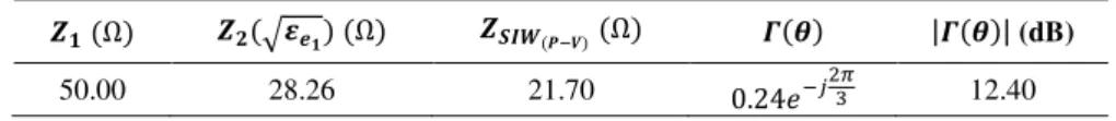
With √ and all the physical dimensions obtained, the impedance values, and the reflection
coefficient calculated considering central frequency of 10.33 GHz can be written in Table VIII.
Table VIII. Impedance values and reflection coefficient for the application example in X Band.
Ω √� Ω �� �− Ω � � |� � | (dB)
50.00 28.26 21.70 . − � 12.40
Fig. 4 Structure built to operate in X Band.
The measurement setup for the structure operating in X Band is shown in Fig. 5.
Fig. 5 Structure built to operate in X Band.
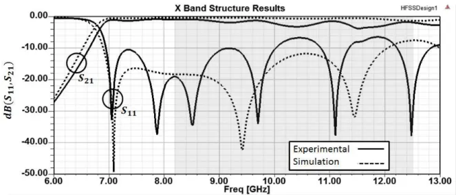
The simulated and measured S parameters obtained for the structure operating in X band are shown
in Fig. 6.
Fig. 6 S parameters obtained for the structure built to operate in X Band.
The simulation results indicated return losses better than 10.0 dB in almost the whole recommend
bandwidth. The experimental results presented some degradation in comparison with the simulated
ones. The calculated value of the reflection coefficient is -12.40 dB, which this match with the
B. Application example considering Ku Band
This application example is designed on RT/duroid 5880. According with Section II, the feeding
line and substrate integrated waveguide physical dimensions are shown in Table IX.
Table IX. Feeding line and SIW physical dimensions for application example in Ku Band.
� (mm) � (mm) � (mm) (mm) (mm) � (mm) � (mm) � (mm)
0.51 1.55 3.58 11.44 1.00 1.50 16.00 27.00
According with the physical dimensions in Table IX, the SIW component operates in a bandwidth
given by (4) and central frequency is given by (5).
. < < . �
= . �
According with the proposed approximation in this research work, the effective dielectric constant
for the feeding line and taper transition is
= .
The central frequency and the effective dielectric constant can be used in (21) and (22) to obtain the
taper transition physical dimensions, as shown in Table X.
Table X. Taper transition physical dimensions for application example in Ku Band.
� (mm) � (mm) � (mm) � (mm)
0.51 1.55 2.48 4.96
With √ and all the physical dimensions obtained, the impedance values, and the reflection
coefficient calculated considering central frequency of 14.75 GHz can be written Table XI.
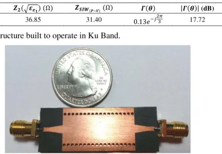
Table XI. Impedance values and reflection coefficient for the application example in Ku Band.
Ω √� Ω �� �− Ω � � |� � | (dB)
50.00 36.85 31.40 . − � 17.72
Figure 7 shows the structure built to operate in Ku Band.
The measurement setup for the structure operating in Ku Band is shown in Fig. 8.
Fig. 8 Structure built to operate in Ku Band.
The simulated and measured S parameters obtained for the structure operating in Ku band are
shown in Fig. 9.
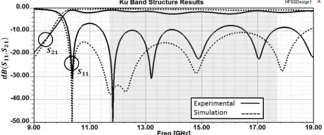
Fig. 9 S parameters obtained for the structure built to operate in Ku Band.
The simulation results indicated return losses better than 10.0 dB in almost the whole recommend
bandwidth. The experimental results presented some degradation in comparison with the simulated
ones. The calculated value of the reflection coefficient is -17.72 dB, which this match with the
experimental results.
V. CONCLUSION
This research work has focused on integration between planar circuits and SIW components. To
connect both structures and realize the impedance matching was considered a taper transition. An
empirical design procedure based on an approximation according with simulation results and
electromagnetic theory was developed to determine the physical dimensions of this particular planar
The proposed approximation in this paper according with simulation results shows an error lower
than % for the wavelength of an electromagnetic wave being propagated along the taper transition
and an error lower than 7% in the impedance matching between the taper transition and the substrate
integrated waveguide. The low error obtained allowed the development of two equations to determine
the width � and length of the taper transition.
The designed procedure developed in this paper was applied in two different structures, which the
first one operates in X Band and the second one operates in Ku Band. For the structure operating in
X Band, the S parameters obtained experimentally shows return loss better than 10.0 dB over 61.67%
of the considered bandwidth. The insertion loss is better than 1.90 dB in almost the whole considered
bandwidth. For the structure operating in Ku Band, the S parameters obtained experimentally shows
return loss better than 10.0 dB over 72.88% of the considered bandwidth. The insertion loss is also
better than 1.96 dB in almost the whole considered bandwidth. The proposed design procedure has
presented good frequency response. Optimization processes can be realized to improve the final
results in the considered structures.
ACKNOWLEDGMENT
The author would like to thank the São Paulo Research Foundation (FAPESP) for the financial
support related to research project with process number 2014/10030-7.
REFERENCES
[1] X. P. Chen, K. Wu, “Substrate Integrated Waveguide Filter,” IEEE Microwave Magazine, vol. 15, no. 5, pp. 108-116, July-Aug. 2014
[2] Y. Cassivi, et al, “Dispersion Characteristics of Substrate Integrated Rectangular Waveguides,” IEEE Microwave and Wireless Components Letters, vol. 12, no. 9, pp. 333-335, Sept. 2002.
[3] T. Shahvirdi and A. Banai, “Applying Contour Integral Method for Analysis of Substrate Integrated Waveguide
Filters,” Microwave Symposium (MMS)-2010 Mediterranean, 2010, pp. 418- 421.
[4] D. Deslandes, K. Wu, “Accurate Modeling, Wave Mechanisms, and Design Considerations of a substrate Integrated
Waveguide,” IEEE Transactions on Microwave Theory and Techniques, vol. 54, no. 6, pp. 2516-2526, June 2006.
[5] F. Xu, K. Wu, “Guided-Wave and Leakage Characteristics of Substrate Integrated Waveguide,” IEEE Transactions on
Microwave Theory and Techniques, vol. 53, no. 6, pp. 66-73, Jan. 2005.
[6] M. Bozzi, L. Perregrini, K. Wu, “Modeling of Conductor, Dielectric, and Radiation Losses in Substrate Integrated
Waveguide by the Boundary Integral-Resonant Mode Expansion Method,” IEEE Transactions on Microwave Theory and Techniques, vol. 56, no. 12, pp. 3153-3161, Dec. 2008.
[7] S. Dermain, D. Deslandes, K. Wu, “Development of Substrate Integrated Waveguide Power Dividers,” Canadian
Conference on Electrical and Computer Engineering- IEEE CCECE 2003, 2003, vol.3, pp. 1921-1924.
[8] C. Wang, W. Che, P. Russer, “High Isolation Multi-way Power Dividing/Combining Network Implemented by
Broadside- Coupling SIW Directional Couplers,” International Journal of RF and Microwave Computer, vol. 19, no. 5, pp. 577-582, Sep. 2009.
[9] C. Wang, et al, “Multi-way Microwave Planar Power Divider/Combiner Based on Substrate Integrated Rectangular
Waveguides Directional Couplers,” International Conference on Microwave and Millimeter Wave technology, Nanjing,
2008, pp. 18-21.
[10]D. Deslandes, “Design Equations for Tapered Microstrip-To-Substrate Integrated Waveguide Transitions,” Microwave
Symposium Digest (MTT)-2010 IEEE MTT-S International, 2010, pp. 704-707.
[11]D. Deslandes, K. Wu, “Integrated Microstrip and Rectangular Waveguide in Planar Form,” IEEE Microwave and Wireless Components Letters, vol. 11, no. 2, pp. 68-70, Feb. 2001.
[12]S. Ramo, J. R. Whinnery, T.V. Duzer, “Waveguides With Cylindrical Conducting Boundaries,” in Fields and Waves in
Communication Electronics, 3rd ed., USA: John Wiley & Sons, Inc., 1994, pp. 417-428.
[13]D. M. Pozar, “Transmissions Lines and Waveguides,” in Microwave Engineering, 4th ed., USA: John Wiley & Sons,
Inc., 2012, pp. 147-153.
[14]D. M. Pozar, “Impedance Matching and Tuning,” in Microwave Engineering, 4th ed., USA: John Wiley & Sons, Inc.,