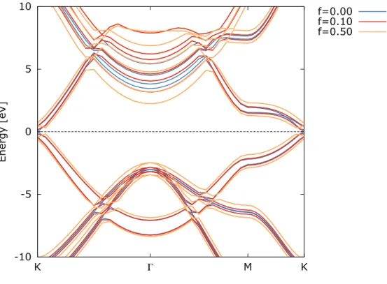
Electric Gap Control in a Semiconductor
Texto
Imagem

Documentos relacionados
This paper focu- ses specifi cally on component-based middleware, i.e., the software layer that offers, to application developers, a platform, a programming model and a standard set
No entanto, a riqueza (e dificuldade) matem´ atica das equa¸c˜ oes de Becker-D¨ oring aliadas ao facto de que algumas das propriedades das suas solu¸c˜ oes serem provavelmente
The server of the system has three layers, the upper layer (interface layer) to receive and answer to clients requests, an intermediate layer (coordination layer) for coordination
Apesar dos dispositivos de pedagogização lançados pelas tecnologias, principalmente a Televisão e Internet, não cabe à escola negá-las, pois isto levará a
Dois estudos recentes – um do Banco Mundial e outro de Freedom House ou Heritage Foundation – mostram de forma clara que a globalização ou inserção na economia mundial com abertura
The probability of attending school four our group of interest in this region increased by 6.5 percentage points after the expansion of the Bolsa Família program in 2007 and
Particularly for the Euro area, researchers have then turned their focus to the impact of the EMU on those stylized facts, and, more recently, on the functioning of the
on the response recorded extracellularly from the olfactory nerve (lower trace) and its integrated activity (upper trace), and (B) the subsequent trace of a similar long-term
