Near-edge X-ray absorption spectroscopy signature of image potential
states in multilayer epitaxial graphene
P.M. Coelho
a, D.D. dos Reis
a, M.J.S. Matos
a, T.G. Mendes-de-Sa
a, A.M.B. Goncalves
b, R.G. Lacerda
a,
A. Malachias
a, R. Magalhaes-Paniago
a,⁎
aDepartamento de Fisica, Universidade Federal de Minas Gerais, Belo Horizonte, MG, CEP 30123-970, Brazil bInstituto de Fisica, Universidade Federal do Mato Grosso do Sul, Campo Grande, MS, CEP 79070-900, Brazil
a b s t r a c t
a r t i c l e
i n f o
Article history:
Received 7 August 2015 Accepted 9 October 2015 Available online 19 October 2015
Keywords:
Graphene Graphite Microscopy Spectroscopy Diffraction
Single layer behavior in multilayer epitaxial graphene has been a matter of intense investigation. This is due to the layer decoupling that occurs during growth of graphene on some types of substrates, such as carbon-terminated silicon carbide. We show here that near-edge X-ray absorption spectroscopy can be used to observe the signature of this decoupling. To this end, samples of multilayer graphene from silicon carbide sublimation were grown with different degrees of decoupling. Raman spectroscopy was used to infer the degree of structural decoupling. X-ray grazing-incidence diffraction and scanning tunneling microscopy showed that growth initiates with the presence of bilayer graphene commensurate structures, while layer decoupling is associated to the formation of incommensurate structures observed for longer sublimation time. Near-edge X-ray absorption spectroscopy was used to probe the electronic states above the Fermi energy. Besides theσ* andπ* empty states, image potential states are observed and show a clear change of intensity as a function of incident angle. These image potential states evolve from a graphite- to graphene-like behavior as a function of growth time and can be used to infer the degree of structural coupling among layers.
© 2015 Elsevier B.V. All rights reserved.
1. Introduction
Graphene is a novel material with electronic properties that are quite unique if compared to other condensed matter systems[1]. Its two-dimensional honeycomb structure composed of carbon hexagons makes it a semimetal where the electrons exhibit a linearly dispersing behavior. The case of an isolated sheet of graphene is easily understood, but once this sheet is in contact with a substrate or stacked on top of other graphene sheets, its behavior changes dramatically and has been a matter of intense investigation[2]. In special, the case of multilayer graphene (a pile of misoriented graphene sheets, where the stacking may or may not be well-defined) is extremely difficult to analyze.
It is well-known that multilayer epitaxial graphene can be grown by sublimation of silicon carbide substrates[3]. Such process takes place when the substrate is heated at a temperature where the silicon atoms desorb from the surface leaving a graphene layer behind. Once such graphene multilayer is formed an intricate stacking may be observed on the sample surface. If this desorption procedure is carried out while heating the carbon-terminated surface of silicon carbide [SiC(000-1)] in an environment of argon, the graphene layers exhibit an isolated graphene Raman signature[3].
One of the difficulties in working with epitaxial graphene is the correct identification of its behavior as two-dimensional (similar to graphene) or three-dimensional (graphite). The different behavior is a consequence of the stacking, which may result in distinct degrees of structural coupling. While graphite is formed by graphene layers which are AB stacked, multilayer graphene is composed of layers which do not show any specific type of stacking. If the layers do not form any type of defined structure[4], multilayer graphene exhibits a clear two-dimensional behavior, although being formed by several graphene layers. This can be observed using Raman scattering[5]or scanning tunneling microscopy (STM)[6], each technique with its advantages and drawbacks. While Raman spectroscopy lacks spatial resolution below ~500 nm, STM is a local technique (lacking statistical information) which only reveals the surface structure and is not completely reproducible due to tip preparation effects.
X-ray near-edge absorption spectroscopy (NEXAFS) performed at the carbon K-edge[7–15]could in principle be used, since it may yield a variable spatial resolution ranging from a few nanometers to millime-ters. The differentiation of multilayer graphene from graphite is more difficult, since both have very similar NEXAFS spectra[9–11]. The NEXAFS spectra of graphene/graphite revealσ* andπ* empty states right above the Fermi energy[7], which have essentially the same ener-gy signature. Besides these two very clear states, a number of additional peaks have been identified by Pacilé et al.[11]from few-layer graphene, such as a pre-peak right above the Fermi energy and an additional ⁎ Corresponding author. Tel.: +55 31 34096625.
E-mail address:[email protected](R. Magalhaes-Paniago).
http://dx.doi.org/10.1016/j.susc.2015.10.016
0039-6028/© 2015 Elsevier B.V. All rights reserved.
Contents lists available atScienceDirect
Surface Science
feature 4 eV above the Fermi energy, in between theσ* andπ* peaks. The origin of this additional peak,first identified as an interlayer state [11,12,15,16], was clarified by Bose et al.[17]. It is associated with the presence of an intersheet hybridization of thefirst even image potential state which is an unoccupied electronic state with nearly free electronic properties. These states have a clear signature difference between monolayers and bilayers of graphene and also graphite[17–19]. Hybrid-ization of graphene with the underlying substrate was also identified using NEXAFS[13,14]. In fact, Schultz et al.[14]have already used the signature of NEXAFS to obtained energy resolved micrographs of graphene deposited on copper and identify its interaction with the substrate atoms.
2. Materials and methods
In this work, three multilayer graphene samples were grown for 30, 45 and 60 min to observe the decoupling of graphene layers. The samples were grown by heating silicon carbide in a resistive furnace at 1780 °C under argon atmosphere. Thefirst signature of coupling was obtained by a Raman spectroscopy analysis of the 2D band of all samples. X-ray grazing-incidence scattering was used to observe the orientational order of neighboring graphene layers, which is deter-mined by the layer stacking. Starting from perfect order (AB stacking), the formation of bilayer commensurate structures with specific angles was observed. The stacking of the 30 min sample was studied by STM where most commensurate structures were measured, and the onset of the formation of incommensurate structure (a signature of graphene behavior) was also observed.
Our samples were grown by SiC sublimation at 1780 °C. The SiC(000-1) substrate was carbon terminated 4H-SiC purchased from Cree Incorporated (www.cree.com). The sample substrates werefirst annealed at 1700 °C for 10 min in a hydrogen atmosphere, to obtain atomicallyflat terraces, as confirmed by atomic force microscopy. The three samples were then obtained by annealing the substrate at T = 1780 °C in an argon atmosphere (pressure of 1 atm), with sublima-tion times of 30, 45 and 60 min. (for growth details see[4]). The mea-surements of Raman spectra were carried out using a Delta Nu Examiner 532 spectrometer with an Olympus BX51 microscope with a 100 × objective lens and a visible laser of wavelength 532 nm. The X-ray Diffraction collection of data was carried out at the Brazilian National Laboratory of Synchrotron Light (LNLS) at beamline XRD2, a bending magnet X-ray source with aflux of 1010photons/s and an
X-ray wavelength of 0.1549 nm. STM measurements were done at room temperature using an Omicron Variable Temperature Microscope (VT-AFM) with an electrochemically etched tungsten tip and an ultra-high vacuum chamber with a base pressure better than 2.0 × 10⁻¹⁰ mBar. Prior to measurements all samples were degassed by a heat treat-ment of 200 °C for one hour to eliminate sample contamination. All samples were cooled down to room temperature before measurements. Near-edge X-ray absorption spectroscopy was used to study the electronic states above the Fermi energy. Our NEXAFS measurements were performed for all samples under ultra-high vacuum conditions (better than 2 × 10⁻¹⁰mBar) at the soft X-ray PGM beamline of LNLS. This variable line spacing grating undulator beamline (Apple II - type) delivers a photonflux of 1011photons/s with an energy resolution
E/ΔE = 6000[20]. Measurements were performed for a limited inci-dent angle range ofδ= 0° toδ= 30°, (where 0° corresponds to normal incidence, see inset ofFig. 3). The absorption was detected by total elec-tron yield. Besides theσ* andπ* empty states, image potential states were observed and showed a clear change of intensity as a function of incident angle and structural coupling.
3. Results
Raman spectra near the 2D peak of these 3 samples are shown in Fig. 1(a). The 2D peak exhibits a clear narrowing as growth time
increases, which is a signature of layer decoupling[3]. In the case of the sample grown for 30 min, the Raman spectrum is actually the composition of several Lorentzian peaks corresponding to different resonance processes from the band of graphite[6]. As time increases, it clearly becomes narrower with a linewidth of 27 cm−1for 60 min, approximately the value for single layer graphene (25 cm−1)[6]. This result essentially shows that the decoupling of the layers of carbon increases with growth time and the behavior for the topmost layers of the sample grown for 60 min is that of graphene with a single Raman scattering process.
A clearer structural picture of layer decoupling is achieved using grazing-incidence X-ray diffraction. InFig. 1(b) we present the geome-try of rotation scans that were used to identify the stacking between subsequent graphene layers. The incident X-ray beam (green) was positioned in a grazing angleα= 0.25°. In this geometry the diffraction is due to atomic planes lying perpendicularly to the surface, and the diffracted beam was collected by the detector (also in green) in a grazing exit angleβ= 0.25° with respect to the sample surface, with a horizontal diffraction angle 2θ= 42.628°, with respect to the incident
beam, corresponding to the graphene (100) diffraction peak.
The sample was rotated around its azimuthal axisωwith the detec-torfixed to observe the angle of rotation between graphene layers. In Fig. 1(c–e) these rotation scans are shown. For the sample grown for 30 min(1(b)) there are peaks at very specific angles such as 3.89°,
6.01°, 7.34°and 9.43°. These peaks correspond to angles where
com-mensurate structures are formed between two subsequent graphene layers[4]. They correspond to stacking configurations where the superstructure periodicity is a multiple of the graphene atomic period. One can notice that for the sample grown for 30 min the AB stacking (0°rotation angle) exhibits a very strong peak (off-scale), which
corre-sponds to the initial formation of graphite. In the case of samples grown for longer time (45 min [1(c)] and 60 min [1(d)]), the AB stacking is much less pronounced and these specific commensurate angles are not clearly visible. Instead, a diffuse background is visible with no partic-ular stacking. From the X-ray data, however, it is not possible to identify if more than one rotation between graphene layers occurs during the formation of multilayer graphene. The observation of different angles in these scans (for the 45 and 60 min samples) can be due to several rotations of commensurate structures or the presence of other types of stacking, leading to incommensurate structures.
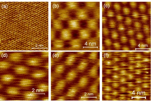
To clarify this issue in detail, STM images of the sample grown for 30 min were taken. InFig. 2(a–f) we show STM images of different regions of the same sample. Several Moiré patterns were observed, and the rotation angleϕfrom subsequent layers was inferred from the observed superstructure periodicity D following the relationship D = a/[2sin(ϕ/2)] and a = 0.246 nm[5]. The values of D were precisely determined via Fast Fourier Transforms (FFTs) of each STM image. An analysis of over 20 STM images showed that about 80% of the rotation angles correspond to commensurate structures. A few incommensurate structures could be identified by STM. WhileFig. 2(a–e) show images of commensurate configurations,Fig. 2(f) present an STM image corre-sponding to a rotation angle ofϕ= 6.4°, showing the formation of few incommensurate structures with layers with a lower degree of coupling.
A striking observation is the lack of atomic resolution in this partic-ular image (2(f)), which was taken with exactly the same tunneling parameters as the others. This result was tested by changing from commensurate to incommensurate regions back and forth and observ-ing the reproducibility of atomic resolution in commensurate regions and lack of it in incommensurate regions, excluding the possibility of a change in the tunneling condition. This is also a signature of loss of structural coupling of subsequent layers at the surface and an indication of the formation of multilayer graphene from incommensurate struc-tures through the layer stack.
An electronic signature of layer decoupling of multilayer graphene may be obtained using near-edge X-ray absorptionfine structure.
Fig. 1.(a) Raman spectra of the samples grown for 30, 45 and 60 min. Note the decrease of the linewidth for longer growth times. (b) Geometry of X-ray grazing incidence diffraction used to identify the rotation angle between graphene layers (see text). Scans along theωdirection for the (100) graphene X-ray peak and samples grown for (c) 30 min, (d) 45 min and (e) 60 min. Note the presence of specific peaks for commensurate structures in the 30 min sample (arrows).
NEXAFS spectra essentially probe empty electronic states starting from a core electron. Energy scans crossing the K absorption edge of carbon (E = 284.2 eV) were performed, focusing in the intermediate region in between the electronic unoccupiedπ* andσ* states. In essence, these scans probe the electronic states above the Fermi energy by promoting a core K-electron to these empty states. Therefore, one can calculate the energy of an observed state above the Fermi energy by subtracting the energy necessary to promote this electron from its core state to the Fermi energy level (i.e., by 284 eV)[7]. Besides theπ* andσ* states, which can be directly calculated from the electronic band diagram of graphene (and have theπandσcounterparts which are occupied), one also probes image potential states which do not have counterparts and are localized in front of the surface in a potential well formed by the band gap on one side and the image potential barrier on the other[17].
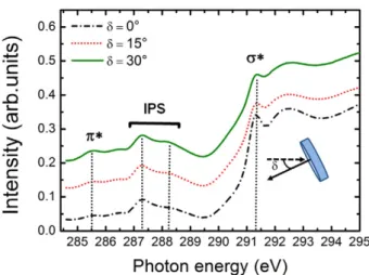
Ourfirst analysis focuses on the correspondence between intensity and incident angleδtaken for the sample of 45 min of growth. As it can be seen inFig. 3, theπ* peak (at 285.5 eV) becomes more prominent asδincreases and we are further away from normal incidence (δ= 0°). On the other hand, theσ* peak (with a first maximum at around 291.3 eV) decreases, showing the effect of the electricfield polarization of the incoming X-ray beam. Theσ* peak is maximized for normal inci-dence (δ= 0°, electronic orbitals lying on the sample surface), whereas
theπ* peak is maximized for grazing-incidence angles (δ= 90°, orbitals
perpendicular to the surface).
More importantly, we observe additional peaks at 287.3 eV and 288.2 eV (also marked by dashed lines). These peaks should be from image potential states (IPS) from graphite or graphene, depending on the sample.
Silkin et al.[19]have already studied image potential states of graphene. They predicted that a double series of Rydberg states with even (n+) and odd (n−) symmetry should exist. The even electronic states have lower energy and are symmetric with respect to the graphene plane while the odd states have a higher energy and are anti-symmetric. They both exhibit intersheet hybridization and are unoccupied states with nearly free electronic properties. Even states are located closer to the graphene layers and are coupled to theσ bands, while odd states are hybridized with theπbands and are located further away from the graphene surface. InFig. 4(a) we present a sche-matic band diagram near theΓpoint where the two image potential states start at energies approximately 3 eV above the Fermi energy. They evolve to higher energies towards both theΚandΜpoints with a parabolic shape and cross theπ* band approximately in the middle of the Brilouin zone.
These image potential states were already observed by scanning tunneling spectroscopy by Bose et al.[17]at specific energies for graph-ite (4.26 eV above the Fermi energy for the 1 state), graphene (3.3 eV for 1+and 3.95 eV for 1−) and bilayer graphene (3.4 eV for 1+and 4.03 eV for 1−). Therefore the peaks should be observed in the NEXAFS spectra approximately at 288.4 eV for the 1 state of graphite, 287.5 eV for 1+of
graphene and 288.2 eV for 1−of graphene[17 –19].
The analysis above leads us to the conclusion that the peak at 288.2 eV observed in the NEXAFS spectra should be a sum of the contri-butions from both the 1 state of graphite as well as 1−of graphene. The peak at 287.3 eV should contain the 1+image potential of graphene. In
order to identify the physical origin of the peaks we have performed an analysis of these image potential states by comparing spectra for differ-ent inciddiffer-ent angles as well as differdiffer-ent samples. InFig. 4(b) we present high resolution spectra of the two peaks for the sample grown for 30 min. The first striking observation is that the spectra do not exhibit any significant intensity variation fromδ= 0°to 30°. This lack
of intensity variation shows that the origin of this signal must be from 3-dimensional carbon bonds. Therefore, the peak at 288.2 eV stems mainly from graphite which, even with the presence of rotated commensurate stacked layers as observed using X-ray diffraction and STM, keeps its 3-dimensional character. The peak at 287.3 eV, however, albeit exactly at the position of the 1+state and considering the lack of
intensity variation as a function of incident angle, cannot be solely explained by this state. Lee et al.[13]performed a similar analysis of graphene on copper and concluded that this peak is also due to edge states of graphene or graphite steps. These edge states have already been observed for amorphous carbon as well[21], and do not exhibit any NEXAFS intensity variation.
The spectra for the sample grown in 60 min, depicted inFig. 4(c), shows a more complex behavior. Asδincreases, the intensity area ratio between the (1 + 1−) peak and the (edge + 1+) peak increases significantly. The behavior of the (1 + 1−) peak is similar to the one of theπ* peak at 285.5 eV. It is consistent with excited states associated with conduction electrons of a two-dimensional material with electron-ic bonds perpendelectron-icular to the graphene sheet. Therefore,the change in intensity of the peak at 288.2 eV should be taken as the signature of forma-tion of multilayer graphene with uncoupled electronic behavior: if it increases as a function of incident angle, the system behaves as multi-layer graphene, otherwise it has a graphite-like behavior. The change in intensity of this peak at 288.2 eV forδ= 30°becomes even clearer
once the NEXAFS spectra of the 3 samples are plotted, as shown on Fig. 4(d). This graph clearly shows an increase of the (1 + 1−) peak as uncoupled multilayer graphene is observed for longer growth times.
The integrated areas of the identified peaks should allow us to eval-uate the evolution of the formation of multilayer graphene. Therefore, we have performed least-squarefits of all NEXAFS spectra. Due to the asymmetric profiles of we have used the method introduced by Outka and Stohr[22]of a Gaussian function with a widthΓdepending linearly upon energy E (i.e.,Γ= E. m + b, using m = 0.575 and b =−164.75 as starting values and limiting their variation to +/−50%). This asymmet-ric function is the correct choice for the lineshape since the NEXAFSfinal state is degenerate with the continuum and therefore one should ob-serve an asymmetric profile with a slightly higher intensities for higher energies. We have found that all NEXAFS peaks are wellfitted by this function with considerable variation in the asymmetry parameters m and b. In essence, the NEXAFS peaks of graphene are considerably broader than the graphite peaks. We also observed a slight variation of the graphite peak lineshape as a function of the angle (as is seen in Fig. 4(b)). InFig. 4(b–d) we show thesefits with peak centersfixed at 287.3 eV, 288.18 eV and 288.30 eV.
InTable 1we present the obtained integrated intensity between the image potential 1 of graphite divided by the (edge + 1+) peak. Corresponding values for the image potential state 1−of graphene are also shown. For the samples grown for 45 and 60 min one observes an increase of the contribution of the 1−graphene peak asδincreases. Fig. 3.NEXAFS measurements as a function of incident angle for the sample grown for
45 min. The lower right inset shows the absorption geometry where the incident X-ray beam is shown as a dashed line.δ= 0° corresponds to normal incidence. Besides theπ* andσ* peaks we observe additional peaks in between them which correspond to image potential states (IPS bracket).
The qualitative observation of the angular behavior of the 1−peak of graphene is therefore confirmed quantitatively. As for the peak 1 of graphite, an increase of the 1/(edge + 1+) ratio is also observed for
longer growth times. This analysis shows that the total amount of graphite also increases as a function of growth time, as observed using X-ray diffraction.
4. Discussion and conclusions
It is possible to compare these results to experimental observations of image potential states in graphite and graphene systems via two-photon photoemission, which also probes unoccupied electronic states
origin of both the initial and thefinal states. In our case the results agree completely with the analysis performed my Bose et al.[17]concerning both peak positions as well as samples characteristics (interplay between graphene and graphite).
One should also discuss possible applications of the NEXAFS signa-ture for the identification of regions with graphene behavior. For instance, surface microscopy of graphene on different substrates using Raman spectroscopy suffers from the lack of spatial resolution in the sub-micron range. One could use scanning X-ray microscopy selecting different energies of the NEXAFS spectrum as a function of incident angle to identify regions with true single layer electronic behavior. The use of the NEXAFS signature presented here would enable the iden-tification of graphene layers in a graphite matrix in an area of a few nm2.
In summary, near-edge X-ray absorption spectroscopy was used to study the electronic states of multilayer graphene and was used to iden-tify the signature of layer decoupling among layers. Image potential states in betweenσ⁎andπ⁎empty electronic states of graphene exhibit a clear variation of intensity as a function of incident X-ray angle. Only with the combination of Raman spectroscopy, X-ray diffraction and scanning tunneling microscopy we could understand the NEXAFS signature from both graphene and graphite. These results should prove important for future studies of the properties of graphene layers either in multilayers or on other substrates used for graphene synthesis.
The authors acknowledge experimental support by LNLS. Financial support was provided by Instituto Nacional de Ciência de Tecnologia (INCT NanoCarbono) . We also acknowledge thefinancial support of CNPq (Grant 302990/2014-3) and FAPEMIG (Grant APQ-00540-13).
References
[1] K.S. Novoselov, A.K. Geim, S.V. Morozov, D. Jiang, Y. Zhang, S.V. Dubonos, et al., Science 306 (2004) 666.
[2] D.N. Basov, M.M. Fogler, A. Lanzara, F. Wang, Y. Zhang, Rev. Mod. Phys. 86 (2014) 959.
[3] J. Hass, F.J. Varchon, E. Millan-Otoya, M. Sprinkle, W.A. de Heer, C. Berger, P.N. First, et al., Phys. Rev. Lett. 100 (2008) 125504.
[4] T.G. Mendes-de-Sá, A.M.B. Goncalves, M.J.S. Matos, P.M. Coelho, R. Magalhaes-Paniago, R.G. Lacerda, Nanotechnology 23 (2012) 475602.
[5] F. Varchon, P. Mallet, L. Magaud, J.-Y. Veuillen, Phys. Rev. B 77 (2008) 165415.
[6] A.C. Ferrari, J.C. Meyer, V. Scardaci, C. Casiraghi, M. Lazzeri, F. Mauri, et al., Phys. Rev. Lett. 97 (2006) 187401.
[7] For a review see, e.g. G. Hahner, Chem. Soc. Rev. 35 (2006) 1244.
[8] J.A. Brandes, G.D. Cody, D. Rumble, P. Haberstroh, S. Wirick, Y. Gelinas, Carbon 46 (2008) 1424.
[9] P.E. Batson, Phys. Rev. B 48 (1993) 2608.
[10]C.-L. Lu, H.-C. Lin, C.-C. Hwang, J. Wang, M.-F. Lin, C.-P. Chang, Appl. Phys. Lett. 89 (2006) 221910.
[11]D. Pacilé, M. Papagno, A.F. Rodríguez, M. Grioni, L. Papagno, C.O. Girit, et al., Phys. Rev. Lett. 101 (2008) 066806.
[12] M. Papagno, A.F. Rodríguez, C.O. Girit, J.C. Meyer, A. Zettl, D. Pacilé, Chem. Phys. Lett. 475 (2009) 269.
[13] V. Lee, C. Park, C. Jaye, D.A. Fischer, Q. Yu, W. Wu, et al., Phys. Chem. Lett. 1 (2010) 1247.
[14] B.J. Schultz, C.J. Patridge, V. Lee, C. Jaye, P.S. Lysaght, C. Smith, et al., Nat. Commun. 2 (2011) 273.
[15] D.A. Fischer, R.M. Wentzcovitch, R.G. Carr, A. Continenza, A.J. Freeman, Phys. Rev. B 44 (2001) 1427.
[16]V.N. Strocov, P. Blaha, H.I. Starnberg, M. Rohlfing, R. Claessen, J.-M. Debever, J.-M. Themlin, Phys. Rev. B 61 (2000) 4994.
[17]S. Bose, V.M. Silkin, R. Ohmann, I. Brihuega, L. Vitali, C.H. Michaelis, et al., New J. Phys. 12 (2010) 023028.
[18] D. Niesner, T. Fauster, J. Phys. Condens. Matter 26 (2014) 393001.
[19] V.M. Silkin, J. Zhao, F. Guinea, E.V. Chulkov, P.M. Echenique, H. Petek, Phys. Rev. B 80 (2009), R121408.
[20] J.C. Cezar, P.T. Fonseca, G.L.M.P. Rodrigues, A.R.B. de Castro, R.T. Neuenschwander, F. Rodrigues, et al., J. Phys. Conf. Ser. 425 (2013) 072015.
[21] J.G. Chen, Surf. Sci. Rep. 30 (1997) 1.
[22] D.A. Outka, J. Stöhr, J. Chem. Phys. 88 (1988) 3539.
[23] N. Armbrust, J. Gudde, P. Jakob, U. Hofer, Phys. Rev. Lett. 108 (2012) 056801.
[24]D. Niesner, Th. Fauster, J.I. Dadap, N. Zaki, K.R. Knox, P.-C. Yeh, R. Bhandari, R.M. Osgood, M. Petrovic, M. Kralj, Phys. Rev. B 85 (2012) 081402(R).
[25] D. Niesner, Th. Fauster, J. Phys. Condens. Matter 26 (2014) 393001. Table 1
Integrated intensity ratio between the peak of the image potential state 1 of graphite and the edge + 1+peak (upper values) and the peak of the image potential state 1−of
graphene and the edge + 1+peak (lower values). The dashed values correspond to peaks
that were not included in thefits.
Growth time 30 minutes 45 minutes 60 minutes
δ = 00
δ = 150
δ = 300
0.88 0.98 1.55
0.98 1.33 2.0
0.05 0.89
1.003 1.10 1.78
0.15 1.25
(Coupled) (Layer decoupling) 1 /(edge + 1+)
1 /(edge + 1+)
1 /(edge + 1+)
1– /(edge + 1+)
1– /(edge + 1+)
1– /(edge + 1+)