Repositório ISCTE-IUL
Deposited in Repositório ISCTE-IUL:
2018-04-23
Deposited version:
Post-print
Peer-review status of attached file:
Peer-reviewed
Citation for published item:
Bisognin, A., Nachabe, N., Luxey, C., Gianesello, F., Gloria, D., Costa, J....Arbabian, A. (2017). Ball Grid Array Module with Integrated Shaped Lens for 5G Backhaul/Fronthaul Communications in F-Band. IEEE Transactions on Antennas and Propagation. 65 (12), 6380-6394
Further information on publisher's website:
10.1109/TAP.2017.2755439
Publisher's copyright statement:
This is the peer reviewed version of the following article: Bisognin, A., Nachabe, N., Luxey, C., Gianesello, F., Gloria, D., Costa, J....Arbabian, A. (2017). Ball Grid Array Module with Integrated Shaped Lens for 5G Backhaul/Fronthaul Communications in F-Band. IEEE Transactions on Antennas and Propagation. 65 (12), 6380-6394, which has been published in final form at
https://dx.doi.org/10.1109/TAP.2017.2755439. This article may be used for non-commercial purposes in accordance with the Publisher's Terms and Conditions for self-archiving.
Use policy
Creative Commons CC BY 4.0
The full-text may be used and/or reproduced, and given to third parties in any format or medium, without prior permission or charge, for personal research or study, educational, or not-for-profit purposes provided that:
• a full bibliographic reference is made to the original source • a link is made to the metadata record in the Repository • the full-text is not changed in any way
The full-text must not be sold in any format or medium without the formal permission of the copyright holders.
Serviços de Informação e Documentação, Instituto Universitário de Lisboa (ISCTE-IUL) Av. das Forças Armadas, Edifício II, 1649-026 Lisboa Portugal
Phone: +(351) 217 903 024 | e-mail: administrador.repositorio@iscte-iul.pt https://repositorio.iscte-iul.pt
Ball Grid Array-Module with Integrated Shaped Lens
for 5G Backhaul/Fronthaul Applications in F-band
Aimeric Bisognin, Nour Nachabe, Cyril Luxey, Frederic Gianesello, Daniel Gloria, Jorge Costa, Carlos Fernandes,
Yuri Alvarez, Ana Arboleya, Jaime Laviada, Fernando Las-Heras, Nemat Dolasha Baptiste Grave, Mahmoud
Sawaby, Amin Arbabian
What is the problem being addressed by the manuscript and why is it important to the Antennas &
Propagation community ?
In this paper, we propose a ball grid array (BGA) module with integrated 3D-printed plastic lens and
dedicated 120 GHz OOK transceiver for 5G Backhaul/Fronthaul applications. The problem to be addressed
is the following: 5G future networks will need backhaul/fronthaul 10Gbps wireless links and it’s mandatory
to design cost-effective and energy efficient solutions. The proposed solution is made of 3D-printed plastic
lens antenna and cheap 7×7×0.362 mm
3BGA module integrating a 2×2 array of aperture-coupled patch
antennas as the source of the lens. The measurement results of the full system confirm the expected
performance of the plastic lens: a -10dB matching and a 28 dBi realized gain from 114 to 140 GHz. The
active measurements allows a Tx/Rx link >12Gbps data transmission with <10-6 BER at nearly 5m. This
link is realized with an energy-efficiency better than 1.6 pJ/b/s which is at least 40 times better than
state-of-the-art high-speed existing TRx’s. Those promising results pave the way for future cost-effective and low
consumption backhaul/fronthaul systems for 5G communications.
What is the novelty of your work over the existing work (100 words)?
So far, several wireless links at 120 GHz have been deployed by various authors with very high Gbps speed
but at the expense of high DC consumption and bulky material which is in turn correspond to weak integration
of the full-system. The novelty of our work lies in the fact that every communicating block has been
optimized in conjunction with all the other nearby elements, strongly taking into account cost and integration
capability. Therefore a Tx/Rx link >12Gbps data transmission with <10-6 BER at nearly 5m. This link is
realized with an energy-efficiency better than 1.6 pJ/b/s which is at least 40 times better than state-of-the-art
high-speed existing TRx’s.
Provide up to three references, published or under review, (journal papers, conference papers,
technical reports, etc.) done by the authors/coauthors that are closest to the present work. Upload them
as supporting documents if they are under review or not available in the public domain. Enter “N.A.”
if it is not applicable.
[1]
A. BISOGNIN, A. CIHANGIR, C. LUXEY, G. JACQUEMOD, R. PILARD, F. GIANESELLO, J.R. COSTA, C.A. FERNANDES, E.B. LIMA, C.J. PANAGAMUWA, W.G. WHITTOW, “Ball Grid Array-Module with Integrated Shaped Lens for WiGig Applications in Eyewear Devices”, accepted for publication in IEEE Transactions on Antennas and Propagation,vol. 64, Issue 3, DOI (identifier) 10.1109/TAP.2016.2517667
[2]
A. BISOGNIN, D. TITZ, F. FERRERO, G. JACQUEMOD, R. PILARD, F. GIANESELLO, D. GLORIA, D. LUGARA, E.B. LIMA, J.R. COSTA, C.A. FERNANDES, C. LUXEY, “Non-collimating MMW Polyethylene Lens Mitigating Dual-Source Offset From a Tx/Rx WiGig Module”, IEEE Transactions on Antennas and Propagation, vol. 63, no. 12, pp. 5908-5913, December2015.
[3] A. BISOGNIN, D. TITZ, F. FERRERO, R. PILARD, C.A. FERNANDES, J. R. COSTA, C. CORRE, P. CALASCIBETTA, J-M. RIVIERE, A. POULAIN, C. BADARD, F. GIANESELLO, C. LUXEY, P. BUSSON, D. GLORIA, D. BELOT, “3D Printed Plastic 60 GHz Lens: Enabling Innovative Millimeter Wave Antenna Solution and System”, IEEE International Microwave
Provide up to three references (journal papers, conference papers, technical reports, etc.) done by
other authors that are most important to the present work. Enter “N.A.” if it is not applicable.
[1] N. Deferm and P. Reynaert, "A 120 GHz fully integrated 10 Gb/s short-range star-QAM wireless
transmitter with on-chip bondwire antenna in 45 nm low power CMOS," IEEE Journal of Solid-State
Circuits, vol. 49, no. 7, pp. 1606-1616, July 2014.
[2] A. Hirata, T. Kosugi, H. Takahashi, J. Takeuchi, H. Togo, M. Yaita, N. Kukutsu, T. Nagatsuma, Y. Kado,
"120-GHz-band wireless link technologies for outdoor 10-Gbit/s data transmission," IEEE Transactions
on Microwave Theory and Techniques, vol. 60, no. 3, pp. 881-895, March 2012.
[3] S. Beer, C. Rusch, H. Gulan, B. Gottel, M. G. Girma, J. Hasch, W. Winkler, W. Debski, T. Zwick, "An
integrated 122-GHz antenna array with wire bond compensation for SMT radar sensors," IEEE
Transactions on Antennas and Propagation, vol. 61, no. 12, pp. 5976-5983, Dec. 2013
Abstract — In this paper, we propose a ball grid array (BGA)
module with integrated 3D-printed plastic lens and dedicated 120 GHz OOK transceiver for 5G Backhaul/Fronthaul applications. The 2×2 array of aperture-coupled patch antennas in the BGA module of 7×7×0.362 mm3 exhibits a -10dB matching over a 38% bandwidth (96-140 GHz), a measured realized gain above 7.8 dBi from 110 to 140 GHz, a fair polarization purity of 20 dB and a total efficiency higher than 55% within the same frequency band. The measurement results of the full system confirm the expected performance of the plastic lens. Especially, the measured |S11| demonstrates a -10dB matching and a 28 dBi realized gain from 114 to 140 GHz. Finally, active measurements allow a Tx/Rx link >12 Gbps data transmission with <10-6 BER at nearly 5 m. This link is realized with an energy-efficiency better than 1.6 pJ/b/s which is at least 40 times better than state-of-the-art high-speed existing TRx’s. Those promising results pave the way for future cost-effective and low consumption backhaul/fronthaul systems for 5G communications.
Index Terms— 5G, backhaul/fronthaul links, 3D-printing,
Dielectric Lens, Organic module, Ball-Grid-Array, Millimeter-wave antennas
I. INTRODUCTION
ireless communications are today essentials in everybody’s daily life. In the never-ending race to deliver higher data rate to the users and simultaneous efficient connections within a given area, the concept of 5G has emerged as a natural evolution of the 4G standard [1-2]. The aim of 5G is definitely to deliver multi-gigabit-per-second data speeds, more capacity and lower latency than today’s wireless systems. In this context, the millimeter-waves and especially the available millimeter frequency (broad) bands are perfect candidates to enable the aforementioned goals. Lots of researchers already started to focus their work at 28 and or 39 GHz as interesting frequencies for the access point link between
the user’s mobile equipment and the base-station [3-6]. For example, Samsung put some efforts to investigate the integration of small antennas into possible user’s devices like smartphones [7-9]. However, another highly important challenge lies in the connectivity between those base stations and even between a base station and the core network. Moreover, it should be stressed that an efficient 5G network implementation will definitely benefit from a high densification of the number of those access points, especially if the wireless link with the user’s is deployed at millimeter-wave (mmW) frequencies. In turn, this observation implies that urban small-cells (micro and femto) will have to replace macro-cell base-stations, therefore increasing the number of the access points and their interconnection in what is called HetNets (heterogeneous networks) [10-12]. Lastly, it should not be forgotten that 5G will definitely rise if a cost-effective deployment solution exists for the cellular operators always willing to minimize costs. This is especially true in the context of small cell since the network density should increase by x10 while available CAPEX to deploy those new equipments will remain flat (driving the cost of wireless equipment to be drastically reduce). Therefore, the infrastructure strategy is definitely of paramount importance. For instance, fiber-optic links between base-stations are not always the best choice due to the high cost of civil-engineering necessary to achieve the interconnection link [13][13].
Wireless backhaul and fronthaul links are possible alternatives to fiber-optic links between small-cells. Existing solutions operate in V (57-66 GHz [14-15] and E-bands (71-76 & 81-86 GHz [16-20]) but if they largely compete with fiber-optic links in terms of cost, they do not yet in terms of data rates [21-22]. They remain a little bit expensive for dense-urban point-to-point deployment. Indeed, around 1-2 Gbps data rates are achievable with E/V band backhaul solutions which is sufficient for 4G standard but might be not enough for the newcomer 5G where 10 Gbps are expected over 100 m. Lastly,
Ball Grid Array-Module with Integrated Shaped
Lens for 5G Backhaul/Fronthaul
Communications in F-band
Aimeric Bisognin, Student member, IEEE, Nour Nachabe, Cyril Luxey, Fellow, IEEE, Frederic
Gianesello, Member, IEEE, Daniel Gloria, Member, IEEE, Jorge Costa, Senior Member, IEEE, Carlos
Fernandes, Senior Member, IEEE, Yuri Alvarez Senior member, IEEE, Ana Arboleya, Jaime Laviada,
Fernando Las-Heras, Senior Member, IEEE, Nemat Dolasha Student member, IEEE, Baptiste Grave,
Student member, IEEE, Mahmoud Sawaby, Student member, IEEE, Amin Arbabian, Senior Member,
IEEE
W
Aimeric Bisognin, N. Nachabe, C. Luxey, are with U. Nice. F. Gianesello, D. Gloria are with STMicroelectronics. J. Costa, C. Fernandez are with Univ. Lisbon. Y. Alvarez, A. Arboleya, J. Laviada, F. Las Heras are with Univ. Oviedo. A. Arbabian, N. Dolasha, B. Grave, M. Sawabi are with Univ. Stanford.
those V and E backhaul and fronthaul links usually exhibit power consumption as high as a dozens of Watts (20-35 W) due to the high complexity modulation scheme chosen to minimize the spectral occupancy and mitigate interferences. Consequently, only few of those backhaul links are indeed deployed today in 4G cellular networks. Moreover, in order to improve the efficiency of the wireless network there is now a trend to pool baseband resources (C-RAN concept) which put additional pressure on the data rate required by fronthaul (10 s of Gb/s may be required depending the configuration).
All these observations demonstrate that cost-effective, energy efficient, high-capacity, easy-to-deploy point-to-point wireless links at mmW are necessary for the proper deployment of the 5G infrastructure. Considering the fact that 10 Gbps data rates might be necessary between small cells or between a small cell and the core network to satisfy the user’s need by 2020 [23], it seems to be a logical approach that researcher, today investigate the next available mmW frequency bands above 100 GHz to achieve suitable backhaul/fronthaul links for 5G standards. Operating above 100 GHz will enable compact low-footprint system solutions that can deliver Gbps for dense deployments and therefore competing with wired solution in many aspects [24]. It should be also noted that traditional wireless systems at 60 GHz use higher-order modulations to maximize spectral efficiency, often at the cost of energy efficiency. As a very large bandwidth is available from 120 to 140 GHz, we can definitely relax the spectral efficiency requirements and enable improved energy efficiency using an OOK system. The compact and wideband system we foreseen for mass-market should be also fully packaged with low-cost flip-chip integrated circuit on an organic substrate that includes an antenna-in-package as we already demonstrated in [25-27]. However, in order to increase the maximum operating distance, a higher gain than the one provided by a simple antenna integrated within a BGA is required The idea is then to use the BGA antenna as a feeding source of an integrated 3D-printed lens. The focus is on a small-footprint fully integrated cost-effective solution which overcome traditional packaging challenges imposed at frequencies above 100 GHz.
In this paper we propose a BGA module with integrated shaped lens and dedicated BiCMOS OOK transceiver for 5G Backhaul/Fronthaul applications in F-band. In Section II, we describe the BGA module technology and the design of an efficient source antenna for a dielectric lens. In section III, we present the design and the fabrication of the plastic lens. In the same section, the optimized dome-lens is measured when being fed by the BGA source. In Section IV, active measurements of a Tx/Rx system arrangement are briefly presented demonstrating promising results for a cost-effective, energy-efficient, 5G backhaul/fronthaul commercial solution. The paper ends by a conclusion and possible future improvements of the integrated system.
II. BGA-MODULE
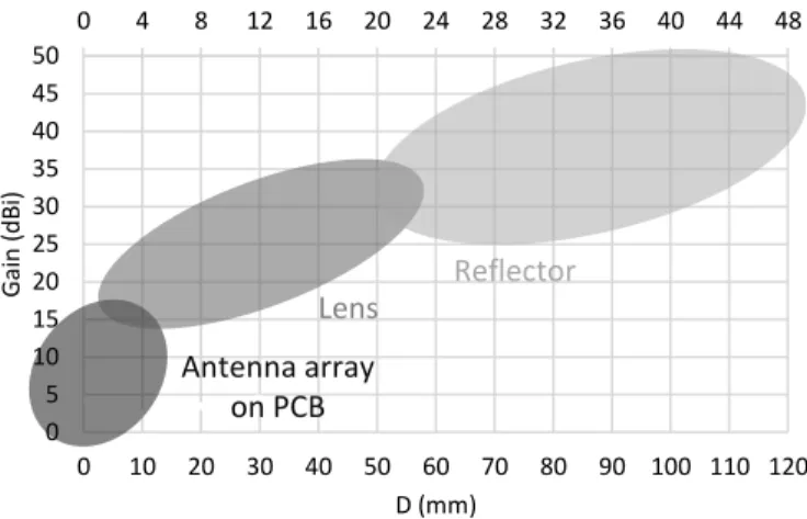
To address the gain requirements of possible 5G backhaul links, we targeted an antenna delivering a 30 dBi gain in the free-licensed 116-142 GHz frequency band. To obtain such a gain, one can think about using a planar antenna on PCB, but the high losses in the microstrip feeding network will limit the achievable gain to near 20 dBi. A more effective way is to use a dielectric lens fed by a planar antenna-source. This would lead to obtain an antenna gain ranging between 20 and 35 dBi (Fig. 1). Ultimately, using a reflector would further increase this gain until 50 dBi at the expense of being bulky. So finally, as a fair compromise between size and performance, we chose to develop a planar antenna integrated in a low-cost Ball Grid Array Module (BGA) as a source of a dielectric elliptical lens.
Fig. 1 Antenna gain versus antenna size D, for different antenna solutions: planar antenna array (D is the length/width of the PCB), lens antenna (D is the diameter of the lens) and reflector (D is the diameter of the reflector). A. F-band Antenna in BGA Packaging Technology
The High Density Interconnect (HDI) technology was developed to address the development of small connected objects. Indeed, the miniaturization of microelectronic components and the increase of the integration density required more advanced technics of fabrication, especially in terms of drawing precision (minimum conductor width and minimum space between conductors…). In addition, operating at frequencies above 50 GHz requires feeding lines and antenna dimensions about ten of microns accurate.
The HDI process is perfectly suited for the design of mmW antennas due to the following reasons:
The standard drawing rules are largely acceptable for the realization of mmW antennas: the minimum conductor width is 50 µm and minimum spacing between conductors is 50 µm (design rules going down to 20 µm being already industrially available).
There is possibility to select low-cost organic substrates with good performance beyond 50 GHz.
The drawing rules and the “strip” format of fabrication of the BGA module allows automatic flip-chip assembly of the chip on the BGA. This has a capital importance considering the mass market we are targeting (5G backhaul/fronthaul links) [28]. 0 4 8 12 16 20 24 28 32 36 40 44 48 0 5 10 15 20 25 30 35 40 45 50 0 10 20 30 40 50 60 70 80 90 100 110 120 D (λ0) at 120 GHz G ai n ( d B i) D (mm) Lens Reflector Antenna array on PCB
The integration scheme is of paramount importance at mm-wave frequencies [29-32]. Our scheme is presented in Fig. 2, the chip is connected in “flip-chip” to the BGA using the copper pillar technology (pad ring pitch < 150 µm). The BGA is then connected to the PCB using sloder balls (diameter 300 µm and pitch 500 µm). The DC signals are routed from the PCB to the BGA through the solder balls and routing lines drawn on the BGA. The antenna is integrated into the multilayer BGA, it radiates in the opposite direction to the chip and BGA. This way the impact of the chip and PCB on the radiation of the antenna is minimized. This type of interconnection enables low-loss transmission between the RF output of the chip and the antenna.
Fig. 2 Antenna-in-package integration scheme.
The build-up (layers) of the BGA module is given in Fig. 3. We chose a standard 1-2-1 HDI build-up consisting in: 1 prepreg simple layer (30 µm thickness) + 1 core double layer (200 µm thickness represented as only one core in Fig. 3) + 1 prepreg simple layer (30 µm thickness). The HDI technology imposes a symmetrical build-up. The DC lines are drawn at M1 (chip and PCB side), as well as the microstrip line. The ground plane is set at P1. Both prepregs are protected by a solder mask.
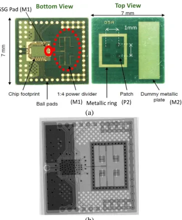
Fig. 3 Cross-sectional view of the 1-2-1 HDI build-up of the BGA module. The BGA module is 7×7×0.362 mm3. A transparent view and pictures of the top and bottom views of the BGA are presented in Fig. 4 and 5. The BGA module integrates a specially designed 2x2 array of four aperture-coupled patch antennas. Each patch of the array is coupled to a microstrip-fed resonant slot in order to maximize the matching and gain bandwidth. The thickness of the prepreg substrates was minimized to increase the coupling between the microstrip line and the slot taking into account the minimum resolution of the HDI technology (50 µm). The slots were set at level P1 and the patches at P2. The 200 µm thickness of the core was chosen to meet the target bandwidth (116 to 142 GHz). The core and prepreg are made
from the same substrate characterized by εr = 3.4 – j*0.01. A 1:4 microstrip divider equally dispatch the power between all array elements and is characterized by an input impedance close to 50 Ω. Spacing between the patches was adjusted to obtain optimal illuminating beamwidth for the chosen elliptical lens: 1 mm (corresponding to 0.43λ0 at 130 GHz) in both x and y transversal directions. The goal was to obtain a Gaussian radiation pattern in both E and H planes of the BGA module with a -10dB level below the maximum within an 80-100° angular region. This particular element arrangement was chosen for a partial cancelation of the TM0 surface wave modes generated by the slots within the core substrate from out-of-phase natural recombination. In addition, the array antenna was surrounded by a grounded metallic ring in order to collect and radiate in phase the residual energy from the TM0 mode with the main radiation of the array antenna.
Fig. 4 Transparent view of all the levels of the BGA module. Bottom view of the module with IC footprint and coupling slots fed by microstrip lines (left side). Top view of the module with 2×2 array of slot-fed patches (right side) with indications of the direction of propagation of TM0 mode generated by the slots.
(a)
(b)
Fig. 5 (a) Top (right) and bottom (left) views of the BGA module integrating the 2x2 antenna array. (b) X ray picture of the BGA module.
Base band PCB mmW TRX BGA Solder ball Copper pillar Antenna Assembly side Radiation side Ground plane Patch Buried Via
Copper (M1) : Microstrip line Copper (P1) : Ground plane
Copper (P2) : Patch Copper (M2) : Metallic ring 200 µm E plane H plane Metallic ring (M2-P1) GSG Pad (M1) (M1) (P2) (M2) 1mm
Bottom View Top View
B. BGA Module Performance in Air
In order to validate our optimized design within the HDI technology, the array antenna of the BGA module radiating in air was measured from 116 to 140 GHz. The BGA module was probe-fed and measured with our customized 3D measurement set-up [33] extended to the F band with mmW extenders [34]. Measured and simulated reflection coefficient fairly agrees in Fig. 6: the |S11| is less than -10 dB from 96 GHz to 140 GHz, representing 38% of bandwidth. This is due to the complementary behavior of the slot, the patch and the metallic ring surrounding the array antenna.
Fig. 6 Simulated and Measured |S11| of the array antenna of the BGA module radiating in air.
Fig. 7 Normalized E and H-plane radiation patterns of the array antenna of the BGA module from 116 to 140 GHz.
The simulated radiation patterns in E (φ =90°) and H (φ =0°) planes for a couple of frequencies within the band are presented in Fig. 7. A quasi frequency constant beamwidth at -10 dB of 88° is maintained from 116 to 140 GHz in H-plane (in fact between 84 and 96°). However, a stronger variation is noticed
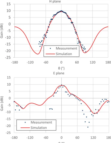
in E-plane even with the careful optimization of the metallic ring for TM0 surface-wave mode management. The beamwidth is what really impacts the elliptical lens illumination and in this sense, the obtained results look satisfactory. A comparison between simulated and measured realized gain co-polarized in E and H-plane radiation patterns at 130 GHz is presented in Fig. 8. A very good agreement is observed in H plane. Aside from the masking effect of the probing system occurring in E-plane, the agreement between simulation and measurement remains fairly acceptable. The measured beamwidth at – 10 dB (relative to the maximum gain) is 90° in H plane and 103° in E plane.
Fig. 8 Simulated and measured realized gain co-polarized radiation pattern in H (ZX) and E (ZY) planes at 130 GHz of the array antenna of the BGA module.
Fig. 9 shows the simulated and measured realized gain in the broadside direction of the top face of the BGA module. The simulated realized gain varies between 9 and 10 dBi from 116 to 140 GHz and the measured realized gain values are very close to the simulated ones (above 7.8 dBi from 110 to 140 GHz). We can remind here the uncertainty of the measurement setup [33-34]: 1.2 dB at 140 GHz. The polarization purity is higher than 20 dB along the F band (90 to 140 GHz). It’s very interesting to notice the gain flatness within the 116-140 GHz. In addition, the antenna has a total simulated efficiency above 66% from 116 to 140 GHz. The measured total efficiency computed from our method described in [35] is estimated to be 55% at 130 GHz. All those module air-measurement results validate the HDI technology and the chosen BGA build-up for an efficient 120 GHz planar source for an elliptical dielectric lens. The next step is the study of the performance of an elliptical lens illuminated by this array antenna source. -40 -30 -20 -10 0 90 100 110 120 130 140 150 |S11 | ( dB ) Frequency (GHz) Simulation Measurement -30 -25 -20 -15 -10 -5 0 -180 -140 -100 -60 -20 20 60 100 140 180 (d B i) Θ° H plane 116 GHz 120 GHz 125 GHz 130 GHz 135 GHz 140 GHz -30 -25 -20 -15 -10 -5 0 -180 -140 -100 -60 -20 20 60 100 140 180 (dB i) Θ E plane 116 GHz 120 GHz 125 GHz 130 GHz 135 GHz 140 GHz -25 -20 -15 -10 -5 0 5 10 15 -180 -120 -60 0 60 120 180 G ai n (dB i) θ (°) H plane Measurement Simulation -25 -20 -15 -10 -5 0 5 10 15 -180 -120 -60 0 60 120 180 G ai n (dB i) θ (°) E plane Measurement Simulation
Fig. 9 Simulated and measured broadside realized gain (co and cross-polarizations) of the array antenna of the BGA versus frequency.
III. DESIGN OF THE LENS A. ABS Material
As we targeted a cost-effective antenna-system for mass-market product, the use of 3D printing technology and material for the fabrication of the elliptical lens is evaluated next. Usually, quartz material [36-37] or high-density polyethylene (HDPE) [38-39] is used for mm-wave lenses above 60 GHz. However, those materials are expensive and need dedicated tooling. Fused Deposition Modeling (FDM) using the ABS-M30 plastic was our finalized choice. So, far, from the best knowledge of the authors, ABS-plastic has been barely used to design/fabricate an antenna operating at frequencies beyond 100 GHz [40]. However, several attempts have been used at lower frequencies [41]. The FDM 3D printing technology consists in the deposition of a thin plastic filament to build layers in an additive manufacturing process. In our case, the in-house machine was able to deliver an ABS-M30 plastic filament of 178 µm diameter. This kind of plastic material is systemically used for the casing of the most common communicating devices (smartphones, cameras, laptops…). Such a dielectric lens could focalize the waves originating from the planar BGA source in a narrow radiated beam and it could be also part of the casing of the backhaul system. In this way, we minimize the negative impact of the casing (radome) on the performance of the antenna and at the same time we have a low-cost system.
In order to use the ABS-M30 material to properly design the elliptical lens, we implemented the measurement method described in [42] to extract its complex permittivity in the 110-125 GHz frequency band. It consists in measuring the complex S11 of a short-circuited waveguide filled with an ABS-M30 plastic sample. The method requires the use of a material sample having the same transversal dimensions as the ones of the waveguide. We used a WR08 waveguide with a length of 50.8 mm and we extruded a parallelepiped ABS-M30 block of
dimensions 2.032×1.016×5 mm3. The plastic sample partially inserted in the WR08 waveguide is shown in Fig. 10. In order to verify the method’s former conditions, we modified the position of the calibration’s reference plane from BB’ to AA’, (Fig. 11) by estimating the propagation constant of the fundamental mode in the waveguide.
Fig. 10 The WR08 waveguide (50.8 mm length) and the ABS-M30 sample partially inserted in the waveguide.
Fig. 11 Measurement and calibration schemes to evaluate the complex permittivity of the ABS-M30.
The impedance of the empty and ABS-filled waveguide at the reference plane AA’ are presented in Fig. 12. As expected, the impedance of the filled waveguide is closer to the center of the smith chart because of the higher (dielectric) losses in the plastic. We also observe a rotation of the impedance curve of the filled waveguide compared to the curve of the hollow waveguide. By applying the optimization algorithm given in [42], we calculated the arc that best fits the impedance curve of the filled waveguide. Determining the position of the center of the curve, the radius and the corresponding phase of the calculated arc, we determined the complex permittivity of the ABS-M30 as εr = 2.49 − j0.027 in the 110-125 GHz frequency band. We also obtained very similar results with the measurement of different samples (actually several disks) from the quasi-optical method developed at ESA/ESTEC [43][43] at 137.5 GHz and we finally decided to use the following permittivity value 𝜀𝑟= 2.48 − 𝑗0.0248. -25 -20 -15 -10 -5 0 5 10 110 115 120 125 130 135 140 (dB i) Frequency (GHz) Simu (Co-Pol) Meas (Co-Pol)
Polynomial interpol. (order 6) Polynomial interpol. (order 6) - 1.2 Polynomial interpol. (order 6) + 1.2 Meas (Cross-pol)
Average noise floor
ABS-M30 sample
(a) (b)
Fig. 12 (a) S11 measurements at AA’ reference plane of the Air-filled and ABS-filled waveguides. (b) comparison between the S11 measurement of the ABS-filled waveguide and the calculated impedance arc at AA’ reference plane. B. ABS Elliptical Lens
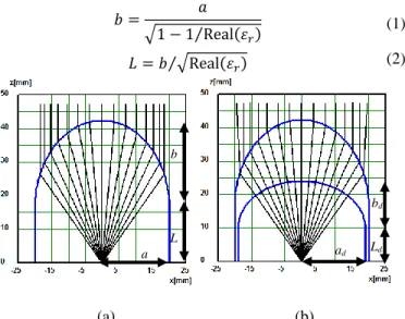
As previously mentioned, the target gain of the antenna of the full system for 5G backhaul links at 120 GHz was set around 30 dBi. This high gain can be obtained by adding an integrated 3D printed dielectric lens on top of the BGA module which is used as a primary feed. A simple single-material lens configuration that at the same time maximizes the achievable gain is the elliptical lens [44]. The elliptical lens, see Fig. 13(a), is defined here by a half ellipsoid with radius a along the x-axis, and a cylindrical extension L from the feed to the center of the ellipse. The ellipse radius along the z-axis is b [44]:
𝑏 = 𝑎
√1 − 1 Real(𝜀⁄ 𝑟)
(1)
𝐿 = 𝑏 √Real(𝜀⁄ 𝑟) (2)
(a) (b)
Fig. 13 (a) Profile and ray tracing of an integrated elliptic lens in ABS material; (b) profile and ray tracing of the dome-type integrated elliptic lens in ABS material.
The radius a should be chosen according to the target directivity in dB which can be estimated from
𝐷𝑖𝑟[𝑑𝐵] = 20 Log10(𝜋𝑎 𝜆⁄ ) (3) where is the operating wavelength. However, gain is affected by the lens dielectric material dissipation losses that can be estimated from (4) [45]
𝐿𝑜𝑠𝑠[𝑑𝐵] = 27.3 √Real(𝜀𝑟) (𝐿 + 𝑏) tan𝛿 𝜆⁄ (4) where L+b is the lens height at the axis and the loss tangent is tan𝛿 = − Imag(𝜀𝑟) Real(𝜀⁄ 𝑟).
Disregarding for now the array antenna (BGA) radiation efficiency, the lens base radius should be chosen so that 𝐷𝑖𝑟 − 𝐿𝑜𝑠𝑠 is around 30dB. For a low cost material compatible with
FDM 3D-printing like ABS (𝜀𝑟= 2.48 − 𝑗0.0248), choosing a=20mm provides a directivity about 34 dB. By using equations (1) and (2), the other lens dimensions become b=25.89 mm and L=16.44 mm. Then, the dissipation loss estimated from (4) is 7.3 dB. Therefore, the directivity of the lens needs to be increased. One possibility is to increase the overall size of the lens that is a radius. But by doing so, the dissipation loss also increases. A much more elegant and efficient approach is to optimize a dome-type elliptical lens with air below the lens to reduce the dissipation losses without reducing its focusing capability and, consequently, its directivity. The simplest dome configuration would have a spherical surface at the feed side with radius ad and centered at the array antenna of the BGA
module. Since one must ensure a lateral wall of ABS material for attaching the IC to the lens, the maximum value for the radius would be ad=19 mm with a 1 mm thick lateral wall. This
would reduce the dissipation path length inside the ABS material to L+b-ad=23.33 mm.
In order to achieve even greater reduction of the path length inside the ABS material, the lower surface of the dome can be chosen to be elliptical instead, with a base radius ad along the
x-axis, a radius bd along the z-axis and a cylindrical extension
Ld, see Fig. 13(b). However, now the radiation from the array
antenna will be refracted at the dome elliptical surface. Therefore, to ensure that the lens does not loose directivity, the dome parameters must be optimized. Using the Genetic Algorithm routine in the ILASH tool [46], those dome parameters were optimized and the results were ad=19 mm,
bd=14 mm and Ld=10 mm. As can be seen in Fig. 13, the ray
tracing of both the full lens and the dome lens present a collimation effect with exiting rays almost parallel to the lens axis. With this dome lens, the height of ABS material in the lens is reduced to L+b-Ld-bd=18.33 mm and by using (4) the
dissipation loss is now estimated to be 3.2 dB. The advantages of this dome lens can be confirmed by performing a full-wave simulation in HFSS software. The results are compared in Fig. 14 with a full (material) elliptical lens. Gain is represented versus a radius, where the dome radius is ad = a – 1 mm. It is
clear that for larger lenses it is very advantageous to use the proposed dome configuration. In fact, for the full ABS-M30 lens there is a radius value where further increasing the radius of the lens does not increase the gain but on the contrary, reduces it due to higher dissipation losses.
Fig. 14 HFSS full-wave simulations of the directivity and gain of a full elliptical lens and a dome elliptical lens (called chopped) of ABS-30 material versus the lens base radius a at 120 GHz.
0 4 8 12 16 20 24 28 32 36 40 44 48 0 10 20 30 40 50 60 (dB i) a (mm)
Directivity and Gain (dBi) vs. lens radius (mm)
Full Ellipitical Lens Directivity Full Elliptical Plastic Lens Gain Chopped Elliptical Lens Gain a
b
L
ad Ld
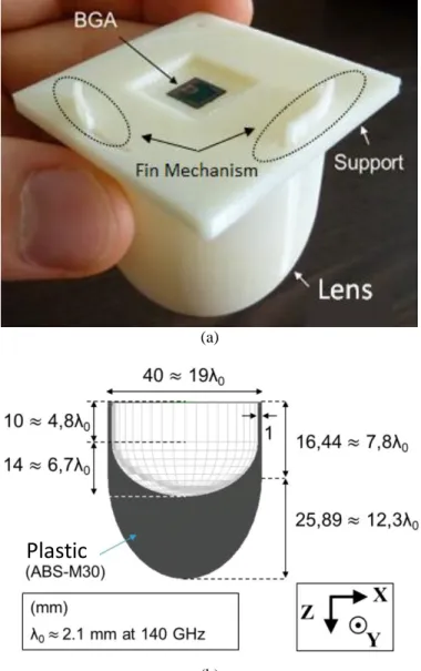
C. Fabrication and measurements of the dome lens
In order to be able to measure the performance of the quasi-optical antenna of the full system composed by the BGA source and the elliptical dome lens, we were forced to use a thin plastic support to place the BGA module at the focal point of the lens (Fig. 15(a)). The support and the dome lens were realized separately by FDM 3D printing and then attached together using the rotating fin mechanism shown in Fig. 15(a). The overall optimized dimensions of the dome lens are given in Fig. 15(b). The BGA module is placed in a cavity within the support. The thickness of the support was optimized to produce the optimal illumination of the dome lens by the array antenna of the BGA module. An HFSS simulation model was elaborated and a parametric study was done to evaluate this best thickness t (Fig. 16).
(a)
(b)
Fig. 15 Description of the elliptical dome lens with BGA source. (a) Picture of the assembly scheme. (b) Overall dimensions of the dome lens.
Fig. 16 HFSS 3D view of the dome lens antenna (left). HFSS model (right) of the BGA source radiating into an ABS-M30 plastic support of thickness t.
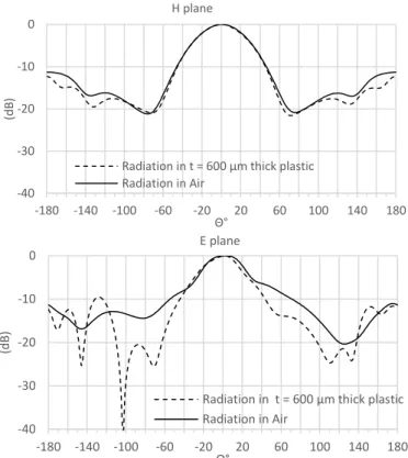
The best performance was found at t = 600 µm giving a |S11| < - 16 dB and a BGA module directivity close to 11 dBi in its broadside direction (Fig. 17). For this thickness t, we show in Fig. 18 the normalized radiation patterns in E (φ =90°) and H (φ =0°) plane at 130 GHz of the array antenna of the BGA source radiating into the plastic support. Those simulated patterns are compared with simulated patterns of the BGA source radiating in the air showing no major disturbance in the Hplane but beneficial differences in the Eplane where the 10dB beamwidth is interestingly reduced. The beamwidth at -10 dB (relative to the maximum directivity) is 80° in both planes and the side lobes level are less than -15 dB in H-plane and -10 dB in E-plane.
Fig.17 Directivity in the broadside direction (plain line) and reflection coefficient |S11| (dotted line) of the HFSS model versus plastic support thickness t at 130 GHz.
The next step was to measure the matching and the radiation pattern of the full antenna system. For this purpose, the antenna measurement setup is given in Fig. 19. The measured |S11| with microelectronic probing reveals a -10dB matching from 114 to 140 GHz and possibly more (20% bandwidth, see Fig. 20). The set-up allows measurement distances from 20 to 60 cm up to 140 GHz. Taking into account the size of the dome lens, D = 40 mm, the far field (FF) distance is RFF = 1.5 m at f = 140 GHz. Thus, we can only perform near-field (NF) measurements and a near-field to far-field (NF-FF) transformation is required to obtain the FF radiation patterns from NF measurements.
Lens
Plastic
-18 -16 -14 -12 -10 -8 -6 -4 -2 0 0 2 4 6 8 10 12 14 0.2 0.4 0.6 0.8 1 S 11 (dB ) Di rec ti vi ty ( dB i) Plastic thickness (µm)Fig. 18 Normalized radiation patterns of the BGA module radiating through the support thickness of 600 µm (dotted lines) and in the air (plain lines) in E and H planes at 130 GHz.
Fig. 19 Upper plot: scheme of the measurement setup. Lower picture: measurement setup arrangement and mounting.
Fig. 20 Measured |S11| of the full antenna system: BGA source radiating into the plastic support and the dome lens.
Positioning accuracy and thermal stability requirements at F-band are very demanding, increasing the cost and complexity of the measurement setup. For this purpose, phaseless techniques are more suitable (and realistic) than complex acquisition. There are two main approaches for phase retrieval: on the one hand, interferometric techniques, where the operating principle is the interference created by a known reference source and the Antenna-Under-Test (AUT) [47-48]. These techniques are accurate and iteration-free, requiring additional hardware to create the interference pattern. On the other hand, iterative techniques, which rely on the information provided by the spatial variation of the NF with distance, require the acquisition of the field on two or more surfaces [49-50]. The main limitation is the risk of stagnation due to the use of iterative solvers for non-linear system of equations.
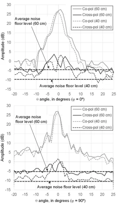
The measurement setup depicted in Fig. 19 cannot be easily modified to allow the use of interferometric techniques, so an iterative phase retrieval method [50] has been considered. Due to mechanical restrictions of the robotic arm, radiated field can be acquired in truncated spherical domains with 1º resolution in both and angles. NF measurement results are depicted in Fig. 21 for f = 140 GHz. It can be noticed that the cross-polar level is close to the average noise floor level, so just the co-polar component at R = 40 and R = 60 cm has been considered for NF-FF transformation. In addition, an asymmetry between = 0º (H-plane) and = 90º (E-plane) cuts can be observed. This artifact is attributed to the BGA source and is the main responsible for the secondary lobes at -15 dB in the = 90º cut. The phaseless NF-FF transformation is outlined in [50]. The goal of the technique is to compute a magnetic current distribution in the aperture from the acquired NF amplitude. For this purpose, a cost function relating the amplitude of the measured field and the amplitude of the field radiated by the equivalent magnetic currents at both observation surfaces (R = 40 and R = 60 cm) is set. This cost function is non-linear, so minimization techniques such as Levenberg-Marquardt that provides monotonic decrease of the error are considered. The iterative solver stops when the error between the iterations n and n+1 is less than 0.001 or if the number of iterations is larger than 50. For this problem, the number of NF samples is 2082 (1041 samples per acquisition surface), and the number of unknowns 841. A GPU implementation of [50] has been developed so the calculation time is less than 10 s overall. -40 -30 -20 -10 0 -180 -140 -100 -60 -20 20 60 100 140 180 (dB ) Θ H plane
Radiation in t = 600 µm thick plastic Radiation in Air -40 -30 -20 -10 0 -180 -140 -100 -60 -20 20 60 100 140 180 (d B ) Θ E plane
Radiation in t = 600 µm thick plastic Radiation in Air
Up & down
Table Right & left Foam
Up & down VDI head
Probe (horn) antenna Lens antenna Robotic arm Mixer Y -40 -35 -30 -25 -20 -15 -10 -5 0 90 94 98 102 106 110 114 118 122 126 130 134 138 |S 11 | (d B ) F (GHz)
Fig. 21 Measured NF at R = 40 cm and R = 60 cm, f = 140 GHz, for the main cuts ( = 0º (H-plane), = 90º (E-plane)). Grey lines: co-polar components. Black lines: cross-polar components.
Next, from the reconstructed equivalent magnetic currents on the lens antenna aperture the FF can be evaluated. Comparison between the lens antenna patterns obtained from simulations and from NF measurements followed by a NF-FF transformation is plotted in Fig. 22 for f = 140 GHz. In the case of the = 0º cut (H plane), there is a good agreement in the main lobe and first sidelobes. However, for = 90º (E-plane) it can be appreciated an increase in the measured sidelobes level which is in agreement with the presence of such sidelobes in the NF pattern (Fig. 21). Directivity is calculated by integrating the radiation pattern, yielding 35.7 dB for simulation results, and Dlens,FF = 32.8 dB in the case of NF measurements followed by a NF-FF transformation. This 2.9 dB difference is mainly due to the higher sidelobes in the measurement results.
The lens antenna gain has been obtained by means of the well-known inter-comparison technique [51] with a standard gain horn in the F-band. As lens antenna gain is measured in the NF region, NF-FF compensation has to be applied (5):
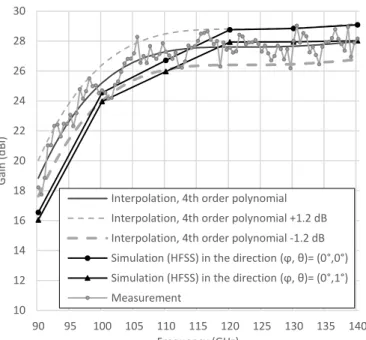
𝐺𝑙𝑒𝑛𝑠,𝐹𝐹[𝑑𝐵𝑖] = 𝐺𝑙𝑒𝑛𝑠,𝑁𝐹+ (𝐷𝑙𝑒𝑛𝑠,𝐹𝐹− 𝐷𝑙𝑒𝑛𝑠,𝑁𝐹) (5) where Glens,NF = 26.5 dBi at 140 GHz (Fig. 21), and Dlens,FF = 32.8 dB. Dlens,NF is calculated by integrating NF pattern at 60 cm, yielding Dlens,NF = 31.5 dB. Thus, Glens,FF = 27.8 dBi, only 1.2 dB lower than the value obtained from simulations (Fig. 23, simulation results: 29 dBi at 140 GHz). It should be also noted that we introduced simulated values of the gain with a 1° offset from the broadside direction which is fully in line with the offset observed in 40 and 60 cm NF radiation patterns in Fig. 21 mainly due to alignment inaccuracy.
Fig. 22 Full antenna system radiation patterns at f = 140 GHz. Comparison between simulation and measurement results in E and H plane.
-50 -45 -40 -35 -30 -25 -20 -15 -10 -5 0 -15 -12 -9 -6 -3 0 3 6 9 12 15 N o rm al iz ed di re ct iv it y (dB ) θ (°) H plane NF measurements + NF-FF transformation Simulation (HFSS) -50 -45 -40 -35 -30 -25 -20 -15 -10 -5 0 -15 -10 -5 0 5 10 15 N o rm al iz ed di re ct iv it y (dB ) θ (°) E plane NF measurements + NF-FF transformation Simulation (HFSS)
Fig. 23 Simulated (FF) and measured (NF>>FF & gain compensation) dome lens antenna gain in the F-band. Measurements have been fitted according to a 4th order polynomial.
IV. ACTIVE MEASUREMENTS FOR 5GBACKHAUL/FRONTHAUL LINKS
For 5G point-to-point backhaul links, we integrated the full antenna system with a specially designed transmission (Tx) and Reception (Rx) chip. For a low-cost and low-consumption system and enabling improved energy efficiency, we focused on using simple (and energy-efficient) OOK modulation scheme. The details of the chip are explained in [52]. The TRx chip was mounted on the BGA source and integrated with the 3D printed lens (Fig. 24).
Fig. 24 Complete Antenna-System with Active chip and PC Board for 5G Backhaul links.
An Effective Isotropic Radiated Power (EIRP) of more than 33 dBm was measured for the Tx with the lens (still in the near-field of the antenna-system). In order to perform measurements using a single BERT and also observe the performance in complex mmW channels, a metal reflector was used to close the Tx-Rx loop when transceivers are placed side by side. Even in the complex/non-ideal extended channel formed by the reflector, >12 Gbps data transmission with <10-6 BER was measured at nearly 5 m. This link was realized with an energy-efficiency better than 1.6 pJ/b/s which is at least 40 times better
than state-of-the-art high-speed TRx’s [53-60]. This is partially due to the high EIRP/PDC,TX (>130 times compared to [53-58]) owing to the high gain yet compact antenna-system as well as the energy efficient OOK system. It should be also noted that very interesting photonic-based solutions have demonstrated impressive 20 Gbps data rates at 120 GHz [61-64] and even 100 Gbps data rates at 240 GHz [65] but these solutions are yet not far from being integrated and suffer from high DC consumption too.
V. CONCLUSION
In this paper we proposed a BGA module with Integrated 3D-printed plastic lens and dedicated 120 GHz OOK transceiver for 5G Backhaul/Fronthaul applications. We first described the BGA module technology and the design of an efficient planar source antenna. The integration of a 2×2 array of aperture-coupled patch antennas in the BGA module of 7×7×0.362 mm3 with a proper management of the surface waves allowed to exhibit measured performance inline with simulated one as a -10 dB matching over a 38% bandwidth (96-140 GHz), a realized gain above 7.8 dBi from 110 to 140 GHz with interesting flatness, a very fair polarization purity of 20 dB and a total efficiency higher than 55% within the band of interest. From the best knowledge of the authors, this planar source in BGA technology offers F-band state-of-the-art performance. Then, we presented the design, the fabrication and the measurement of the ABS plastic lens using the BGA module as a source feed. Measurement results, which are in good agreement with simulations, confirmed the expected performance of the lens antenna-system. Especially, a measured |S11| less than -10 dB from 114 to 140 GHz and a 28 dBi realized gain were obtained within the same frequency bandwidth. Finally, active measurements demonstrated data transmission higher than 12 Gbps with a BER less than 10-6 at nearly 5 m. This link was realized with an energy-efficiency better than 1.6 pJ/b/s which is at least 40 times better than state-of-the-art high-speed TRx’s. This is definitely state-of-the art performance partially due to the high EIRP/PDC metrics nowing to the high gain yet compact antenna-system as well as the energy efficient OOK chosen modulation scheme. We believe those promising results pave the way for future, cost-effective, low consumption backhaul/fronthaul systems for 5G communications. However, the search is not over as future prototypes will definitely have to operate over higher communication ranges in order to be commercially competitive. To achieve this goal several improvements will have to be accomplished. The performance of the circuits could be further improved at first. The performance of the source antenna could be also improved in terms of radiation pattern stability and total efficiency. For example, 3D printed horn fabricated with SLS or stereolithography technology could definitely improve the total efficiency until 90% as demonstrated in [66]. Finally, as depicted in Fig. 1, the lens antenna could be replaced by a reflector approach to substantially increase the gain of the radiating system until 45-50 dBi (enabling proposed system to target link above 100 m). Very promising low-cost antenna-reflector performance have already been obtained, still using 3D-printed technology and simple metallic spray at 60 and 120 GHz [67]. 10 12 14 16 18 20 22 24 26 28 30 90 95 100 105 110 115 120 125 130 135 140 G ai n (dB i) Frequency (GHz) Interpolation, 4th order polynomial Interpolation, 4th order polynomial +1.2 dB Interpolation, 4th order polynomial -1.2 dB Simulation (HFSS) in the direction (ϕ, θ)= (0°,0°) Simulation (HFSS) in the direction (ϕ, θ)= (0°,1°) Measurement
REFERENCES
[1] Y. Niu, Y. Li, D. Jin, L. Su, and A. V. Vasilakos, “A survey of millimeter wave (mmWave) communications for 5G: opportunities and challenges,” Wireless Networks, vol. 21, no. 8, pp 2657–2676, November 2015. [2] L. Frenzel, “5 Things you should know about 5G cellular.” Microwawes
and RF [Online]. Available: http://mwrf.com/blog/5-things-you-should-know-about-5g-cellular. [Accessed: 2-Jan-2017].
[3] T. Rappaport, “Industry visionary: Q&A.” Microwave Journal, October 2016 [Online]. Available: http://www.microwavejournal.com/articles /27220-industry-visionary. [Accessed: 2-Jan-2017].
[4] J. Kimery, “5G Opens up mmWave spectrum: which frequencies will be adopted?” Microwave Journal. 5G and IoT Supplement, November 2016 [Online]. Available: http://www.microwavejournal.com/articles/27358- g-opens-up-mmwave-spectrum-which-frequencies-will-be-adopted. [Accessed: 02-Jan-2017].
[5] T.S. Rappaport, S. Sun, R. Mayzus, H. Zhao, Y. Azar,K. Wang, G.N. Wong, J.K. Schulz, M. Samimi, F. Gutierrez, “Millimeter wave mobile communications for 5G cellular: it will work!,” IEEE Access, vol. 1, pp. 335–349, 2013.
[6] S. Yost, “mmWave: The battle of the bands”, National Instruments [Online]. Available: http://www.ni.com/white-paper/53096/en/. [Accessed: 2-Jan-2017].
[7] W. Hong, K. H. Baek, Y. Lee, Y. Kim, and S. T. Ko, “Study and prototyping of practically large-scale mmWave antenna systems for 5G cellular devices,” IEEE Communications Magazine, vol. 52, no. 9, pp. 63– 69, Sep. 2014.
[8] W. Hong, K. Baek, Y. G. Kim, Y. Lee, and B. Kim, “mmWave phased-array with hemispheric coverage for 5th generation cellular handsets,” European Conference on Antennas and Propagation (EuCAP 2014), The Hague, Netherlands, pp. 714–716, April 2014.
[9] W. Hong, S.-T. Ko, Y. Lee, and K. H. Baek, “Compact 28 GHz antenna array with full polarization flexibility under yaw, pitch, roll motions,” European Conference on Antennas and Propagation (EuCAP 2015), pp. 1– 3, Lisbon, Portugal, April 2015.
[10] D. Anzaldo, “Backhaul alternatives for HetNet small cells, Part 1.” Microwaves and RF [Online]. Available: http://mwrf.com/systems/backhaul-alternatives-hetnet-smallcells-part-1. [Accessed: 2-Jan-2017].
[11] W. Feng, Y. Li, D. Jin, L. Su, and S. Chen, “Millimetre-wave backhaul for 5G networks: challenges and solutions,” Sensors, vol. 16, no. 6, pp. 892-908, Jun. 2016.
[12] J. G. Andrews, S. Buzzi, W. Choi, S.V. Hanly, A. Lozano, A.C.K. Soong, J.C. Zhang, "What will 5G be?," IEEE Journal on Selected Areas in Communications, vol. 32, no. 6, pp. 1065-1082, June 2014.
[13] RSPG Report on spectrum issues on wireless backhaul, Radio Spectrum Policy Group, European Comission [Online]. Available: http://rspg- spectrum.eu/wp-content/uploads/2013/05/RSPG15-607-Final_Report-Wireless_backhaul.pdf. [Accessed: 2-Jan-2017].
[14] L. Verma, M. Fakharzadeh, S. Choi, “Backhaul need for speed: 60 GHz is the solution,” IEEE Wireless Communications, vol. 22, no. 6, pp. 114–121, Dec. 2015.
[15] T. S. Rappaport, J. N. Murdock, F. Gutierrez, “State of the art in 60-GHz integrated circuits and systems for wireless communications,” Proceedings of the IEEE, vol. 99, no. 8, pp. 1390–1436, Aug. 2011.
[16] B. Ayvazian, “Second generation E-band solutions: opportunities for carrier-class LTE backhaul”, White paper, Heavy Reading [Online]. Available: http://www.huawei.com/au/static/HW-206551.pdf [Accessed: 2-Jan-2017].
[17] E. Johnson, “Mobile data backhaul: the need for E-band,” Mobile World Congress, 2013 [Online]. Available: http://www.microwavejournal.com/ext/resources/whitepapers/2013/febru ary/Sky-Light-Research-E-Band.pdf?1471624980 [Accessed: 2-Jan-2017].
[18] “E-Band millimeter wave technology,” Microwave Link, 11-Oct-2016 [Online]. Available: http://www.microwave-link.com/microwave/e-band-millimeter-wave-technology/ [Accessed: 2-Jan-2017].
[19] A. Ghosh, “The 5G mmWave radio revolution,” Microwave Journal, September 2016 [Online]. Available: http://www.microwavejournal.com/articles/27056-the-5g-mmwave-radio-revolution?v=preview. [Accessed: 2-Jan-2017].
[20] S. Deng, C.J. Slezak, G.R.MacCartney Jr., T.S. Rappaport, “Small wavelengths- big potential: millimeter wave propagation measurements for 5G,” Microwave Journal, Mobile Communications Supplement, November 2014 [Online]. Available:
http://www.microwavejournal.com/articles/23274-small-wavelengths- big-potential-millimeter-wave-propagation-measurements-for-5g?v=preview [Accessed: 2-Jan-2017].
[21] “Small cell millimeter wave mesh backhaul.” White Paper Inter Digital
[Online]. Available:
http://www.interdigital.com/research_papers/2013_01_25_small_cell_mil limeter_wave_mesh_backhaul [Accessed: 2-Jan- 2017].
[22] B. Panzner, “Scheduling conflicts in wireless in-band backhaul for 5G millimeter wave communications,” IEEE Conference on Computer
Communications Workshops
(INFOCOM WKSHPS 2016), pp. 110–111, San Francisco, CA, April 2016.
[23] Microwave towards 2020. Delivering high-capacity and cost-efficient backhaul for broadband networks today and in the future, Ericcson, September 2015 [Online]. Availabe: https://www.ericsson.com/res/docs/2015/microwave-2020-report.pdf [Accessed: 2-Jan- 2017].
[24] D. Cohen, “5G and the IoT: 5 Trends and pmplications,” Microwave Journal, September 2016 [Online]. Available: http://www.microwavejournal.com/articles/27058-g-and-the-iot-5-trendsand-implications. [Accessed: 2-Jan-2017].
[25] A. Bisognin, D. Titz, C. Luxey, G. Jacquemod, R. Pilard, F. Gianesello, G. Goria, C. Laporte, H. Ezzeddine, E.B. Lima, J.R. Costa, C.A. Fernandes, F. Devillers, “Millimeter-wave antenna-in-package solutions for WiGig and backhaul applications”, in Proc. International Workshop on Antenna Technology (IWAT 2015), Seoul, Republic of Korea, 4-6 March 2015. [26] J. Chen, L. Ye, D. Titz, F. Gianesello, R. Pilard, A. Cathelin, C. Luxey, A.
Ninknejad, “A Digitally Modulated mm-Wave Cartesian Beamforming Transmitter with Quadrature Spatial Combining”, IEEE International Solid-State Circuits Conference (ISSCC 2013), February 17-21 2013, San Francisco, USA.
[27] A. Townley, P. Swirhun, R. Pilard, A. Bisognin, D. Titz, C. Luxey, A. Niknejad, “A 94GHz 4TX-4RX Phased-Array for FMCW Radar with Integrated LO and Flip-Chip Antenna Package”, in Proc. Radio Frequency Integrated Circuits Symposium (RFIC 2016), San Francisco (CA), USA, June 2016.
[28] R. Pilard, D. Titz, F. Gianesello, P. Calascibetta, J.M. Rivière, J. Lopez, R. Coffy, E. Saugier. A. Poulain, F. Ferrero, C. Luxey, P. Brachat, G. Jacquemond, D. Gloria, "HDI organic technology integrating built-in antennas dedicated to 60 GHz SiP solution," IEEE International Symposium on Antennas and Propagation (APS 2012), Chicago, IL, pp. 1-2, July 2012.
[29] S. Beer, C. Rusch, H. Gulan, B. Gottel, M. G. Girma, J. Hasch, W. Winkler, W. Debski, T. Zwick, "An integrated 122-GHz antenna array with wire bond compensation for SMT radar sensors," IEEE Transactions on Antennas and Propagation, vol. 61, no. 12, pp. 5976-5983, Dec. 2013. [30] D. Liu and Y. P. Zhang, "Integration of array antennas in chip package for
60-GHz radios," Proceedings of the IEEE, vol. 100, no. 7, pp. 2364-2371, July 2012.
[31] A. Valdes-Garcia, S.T. Nicolson, J. Lai, A. Natarajan, P. Chen, S.K. Reynolds, J.C. Zhan,D.G. Kam, D.Liu, B. Floyd, "A fully integrated 16-element phased-array transmitter in SiGe BiCMOS for 60-GHz communications," IEEE Journal of Solid-State Circuits, vol. 45, no. 12, pp. 2757-2773, Dec. 2010.
[32] D. G. Kam, D. Liu, A. Natarajan, S. K. Reynolds and B. A. Floyd, "Organic packages with embedded phased-array antennas for 60-GHz wireless chipsets," IEEE Transactions on Components, Packaging and Manufacturing Technology, vol. 1, no. 11, pp. 1806-1814, Nov. 2011. [33] D. Titz, F. Ferrero, C. Luxey, “Development of a millimeter-wave
measurement setup and dedicated techniques to characterize the matching and radiation performance of probe-fed antennas,” IEEE Antennas and Propagation Magazine, vol. 54, pp. 188-203, 2012.
[34] A. Bisognin, D. Titz, F. Ferrero, G. Jacquemod, R. Pilard, F. Gianesello, D. Gloria, C. Laporte, H. Ezzeddine, D. Lugara, and C. Luxey, “Probe-fed measurement system for F-band antennas,” European Conference on Antennas and Propagation (EuCAP 2014), The Hague, Netherlands, pp. 722-726, April 2014.
[35] D. Titz, F. Ferrero, P. Brachat, C. Luxey and G. Jacquemod, “Efficiency Measurement of Probe-Fed Antennas Operating at Millimeter-Wave Frequencies”, IEEE Antennas and Wireless Propagation Letters, vol. 11, pp. 1194-1197, 2012.
[36] J. M. Edwards and G. M. Rebeiz, "High-efficiency silicon RFIC millimeter-wave elliptical slot-antenna with a quartz lens," IEEE International Symposium on Antennas and Propagation (APSURSI 2011), Spokane, WA, pp. 899-902, July 2011,.
[37] A. Artemenko, A. Mozharovskiy, A. Maltsev, R. Maslennikov, A. Sevastyanov and V. Ssorin, "Experimental characterization of E-band two-dimensional electronically beam-steerable integrated lens antennas," IEEE Antennas and Wireless Propagation Letters, vol. 12, no. , pp. 1188-1191, 2013.
[38] H. Gulan, C. Rusch, S. Beer, T. Zwick, M. Kuri and A. Tessmann, "Lens coupled broadband slot antenna for W-band imaging applications," IEEE Antennas and Propagation Society International Symposium (APSURSI 2013), Orlando, FL, pp. 424-425, July 2013.
[39] B. Göttel, M. Pauli, H. Gulan, M. Girma, J. Hasch and T. Zwick, "Miniaturized 122 GHz short range radar sensor with antenna-in-package (AiP) and dielectric lens," European Conference on Antennas and Propagation (EuCAP 2014), The Hague, The Netherlands, pp. 709-713, April 2014.
[40] H. Yi, S. W. Qu, K. B. Ng, C. H. Chan and X. Bai, "3-D printed millimeter-wave and Terahertz lenses with fixed and frequency scanned beam," IEEE Transactions on Antennas and Propagation, vol. 64, no. 2, pp. 442-449, Feb. 2016.
[41] R. Gonçalves, N.B. Carvalho, P. Pinho, “Wireless energy transfer: Dielectric lens antennas for beam shaping in wireless power-transfer applications”, Comptes Rendus Physique, In Press [online]. Available 9 December 2016, http://dx.doi.org/10.1016/j.crhy.2016.11.004.
[42] M.G. Silveirinha, C.A. Fernandes, and J.R. Costa, “A graphical aid for the complex permittivity measurement at microwave and millimeter wavelengths,” IEEE Microwave and Wireless Components Letters, vol. 24, no. 6, pp. 421-234, June 2014.
[43] E. Saenz, L. Rolo, K. van’t Klooster, M. Paquay, and V.V. Parshin, “Accuracy assessment of material measurements with a Quasi-Optical free-space test bench,” European Conference on Antennas and Propagation (EuCAP 2012), Prague, Czech Republic, pp. 149-152, March 2012. [44] D. F. Filipovic, S. S. Gearhart and G. M. Rebeiz, “Double-slot antennas on
extended hemispherical and elliptical silicon dielectric lenses,” IEEE Transactions on Microwave Theory and Techniques, vol. 41, Issue 10, pp. 1738-1749, October 1993.
[45] C. A. Fernandes, J.R. Costa and E.B. Lima, “Dielectric lens antennas,” Chapter in, Handbook of Antenna Technologies, Zhi Ning Chen, Springer, Singapore, 2016.
[46] E. B. Lima, J. R. Costa, M. G. Silveirinha and C. A. Fernandes, “ILASH - software tool for the design of integrated lens antennas,” in IEEE Antennas and Propagation Society International Symposium (AP-S Symp. 2008), Vol. 1-9, New York, pp. 863-866, July 2008.
[47] J. Laviada, A., Arboleya, Y. Alvarez, C. Garcia, F. Las-Heras, “Phaseless antenna diagnostics based on off-axis holography with synthetic reference wave,” IEEE Antennas and Wireless Propagation Letters, Vol. 13, pp. 43-46, 2014.
[48] A. Arboleya, J. Laviada, J. Ala-Laurinaho, Y. Álvarez, F. Las-Heras, A. Räisänen, “Phaseless characterization of broadband antennas,” IEEE Transactions on Antennas and Propagation, Vol. 64, no. 2, pp. 484-495, February 2016.
[49] S.F. Razavi, Y. Rahmat-Samii, “Phaseless measurements over nonrectangular planar near-field systems without probe corotation”, IEEE Transactions on Antennas and Propagation, Vol. 61, no. 1, pp. 143-152, January 2013.
[50] Y. Álvarez, F. Las-Heras, M. R. Pino, “The sources reconstruction method for amplitude-only field measurements,” IEEE Transactions on Antennas and Propagation, vol. 58, no. 8, pp. 2776-2781, August 2010.
[51] IEEE Standard test procedures for antennas, ANSI/IEEE Std 149-1979. [52] N. Dolatsha, B. Grave, M. Sawaby, C. Chen, A. Babveyh, S. Kananian, A.
Bisognin, C. Luxey, F. Gianesello, J. Costa, C. Fernandes, A. Arbabian, “A compact 130GHz fully packaged point-to-point wireless system with 3D-printed 26dBi lens antenna achieving 12.5Gb/s at 1.55pJ/b/m”, IEEE International Solid-State Circuits Conference (ISSCC 2017), February 2017, San Francisco, USA.
[53] C.W. Byeon, C.H. Yoon, C.S. Park, “A 67mW 10.7Gb/s 60GHz OOK CMOS transceiver for short-range wireless communications,” IEEE Transactions on Microwave. Theory and Techniques, vol. 61, no. 9, pp. 3391-3401, September 2013.
[54] Z. Wang, P-Y. Chiang, P. Nazari, C-C. Wang, Z. Chen, P. Heydari, “A CMOS 210GHz fundamental transceiver with OOK modulation,” IEEE J. Solid-State Circuits, vol. 49, no. 3, pp. 564-580, March 2014.
[55] S. Shahramian, M.J. Holvoak, Y. Baevens, “A 16-element W-band phased array transceiver chipset with flip-chip PCB integrated antennas for multi-gigabit data links,” IEEE Radio Freq. Integrated Circuits Symp., 2015.
[56] S.V. Thyagarajan, S. Kang, A.M. Niknejad, “A 240GHz fully Integrated wideband QPSK receiver in 65nm CMOS,” IEEE J. Solid-State Circuits, vol. 50, no. 10, pp. 2268-2280, October 2015.
[57] R. Wu, S. Kawai, Y. Seo, N. Fajri, K. Kimura, S. Sato, S. Kondo, T. Ueno, T. Siriburanon, S. Maki, B. Liu, Y. Wang, N. Nagashima, M. Miyahara, K. Okada, A. Matsuzawa, “A 42Gb/s 60GHz CMOS transceiver for IEEE 802.11ay,” ISSCC Dig. Tech. Papers, Feb. 2016.
[58] K. Tokgoz S. Maki, S. Kawai, N. Nagashima, J. Emmei, M. Dome, H. Kato, J. Pang, Y. Kawano, T. Suzuki, T. Iwai, Y. Seo, K. Lim, S. Sato, L. Ning, K. Nakata, K. Okada, A. Matsuzawa, “A 56Gb/s W-band CMOS wireless transceiver,” ISSCC Dig. Tech. Papers, Feb. 2016.
[59] M. Pierpoint, G.M. Rebeiz, “Paving the way for 5G realization and mmWave communication systems” Microwave Journal, April 2016 [Online]. Available: http://www.microwavejournal.com/articles/26255- paving-the-way-for-5g-realization-and-mmwave-communication-systems?v=preview. [Accessed: 2-Jan-2017].
[60] N. Deferm and P. Reynaert, "A 120 GHz fully integrated 10 Gb/s short-range star-QAM wireless transmitter with on-chip bondwire antenna in 45 nm low power CMOS," IEEE Journal of Solid-State Circuits, vol. 49, no. 7, pp. 1606-1616, July 2014.
[61] T. Kosugi, A. Hirata, T. Nagatsuma and Y. Kado, "mm-wave long-range wireless systems," IEEE Microwave Magazine, vol. 10, no. 2, pp. 68-76, April 2009.
[62] A. Hirata, T. Kosugi, H. Takahashi, J. Takeuchi, H. Togo, M. Yaita, N. Kukutsu, T. Nagatsuma, Y. Kado, "120-GHz-band wireless link technologies for outdoor 10-Gbit/s data transmission," IEEE Transactions on Microwave Theory and Techniques, vol. 60, no. 3, pp. 881-895, March 2012.
[63] H. Takahashi, T. Kosugi, A. Hirata and K. Murata, "Supporting fast and Ccear video," IEEE Microwave Magazine, vol. 13, no. 6, pp. 54-64, Sept.-Oct. 2012.
[64] A. Hirata, J. Takeuchi, J. Hirokawa "120-GHz-band wireless link antenna technologies for polarization multiplexing," European Conference on Antennas and Propagation (EuCAP 2015), Lisbon, Portugal, pp. 1-4, April 2015.
[65] S. Koenig, D. Lopez-Diaz, J. Antes, F. Boes, R. Henneberger, A. Leuther, A. Tessmann, R. Schmogrow, D. Hillerkiss, R. Palmer, T. Zwick, C. Koos, W. Freude, O. Ambacher, J.Leuthold, I. Kallfass, “Wireless sub-THz communication system with high data rate,” Nature Photonics, vol 7, pp. 977-981, October 2013.
[66] A. Bisognin, D. Titz, C. Luxey, F. Gianesello, C.A. Fernandes, J.R. Costa, D. Gloira, C. Del Rio,“3D-Printed Quasi-Optical Antenna-Systems for
Mm-wave Communications”, Proc. 10th European Conf. on Antennas
and Propagation (EuCAP 2017), Paris, France, 19-24 March 2017. [67] A. Bisognin, C. Luxey, F. Gianesello, D. Titz, C.A. Fernandes, J.R. Costa,
“Digital Manufacturing & Rapid Prototyping: Enabling Innovative & Cost Effective Antenna Solution From RF Up to mmW”, Proc. 10th European Conf. on Antennas and Propagation (EuCAP 2016), Davos, Switzerland, 10-15 April 2016.